Jesse Farrell
-
Project Complete
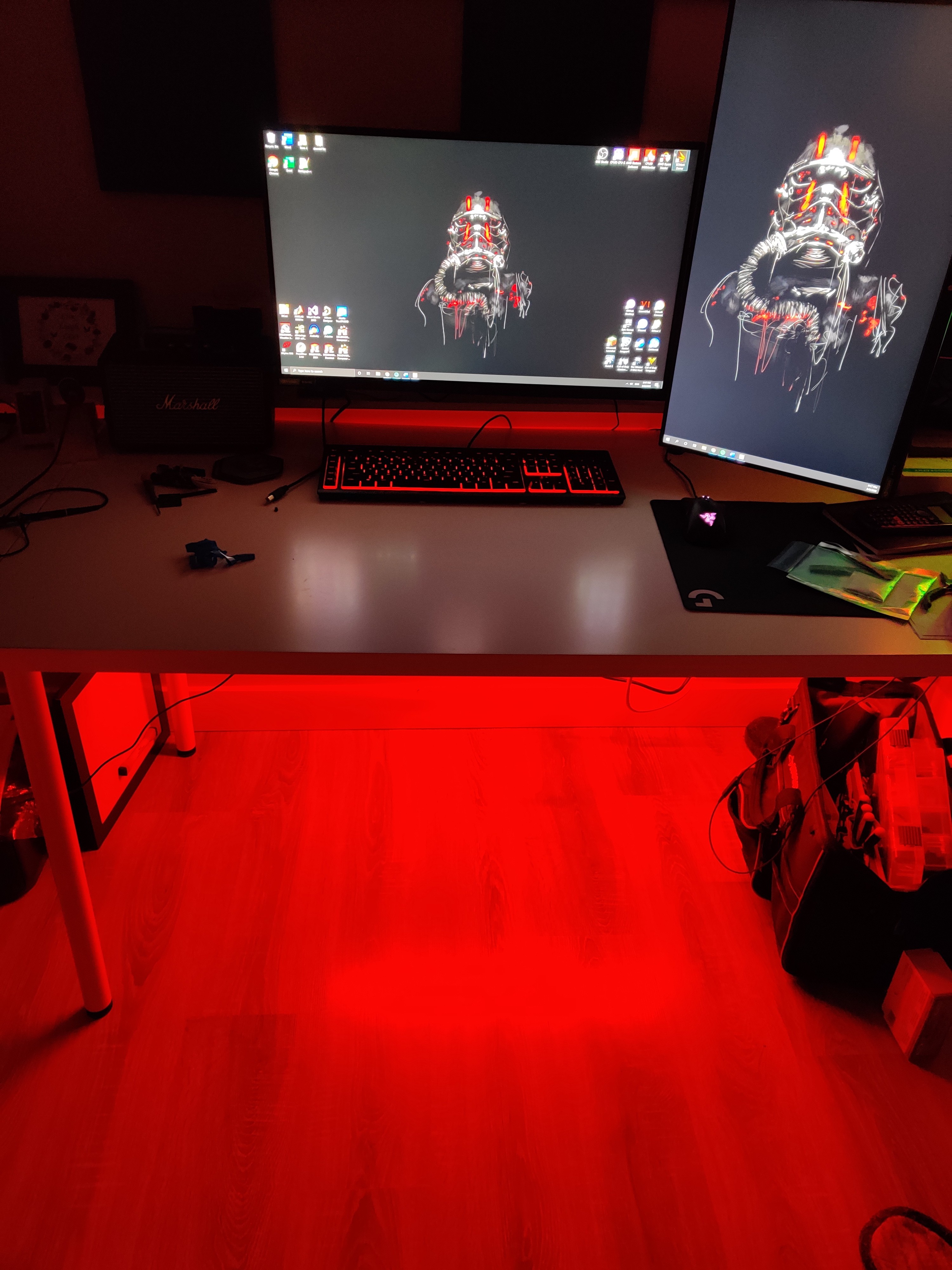
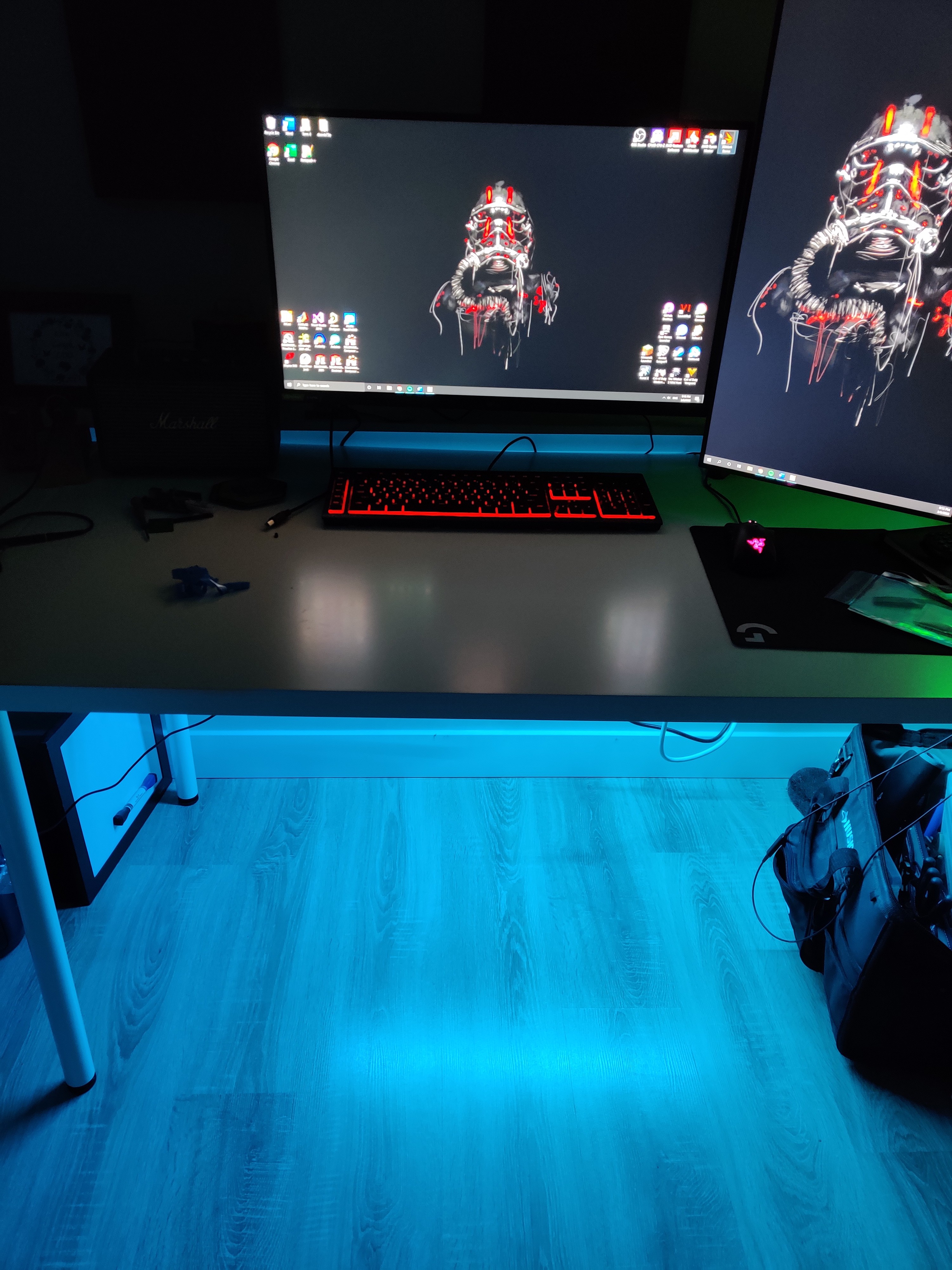
03/09/2022 at 05:30 • 0 commentsJust a quick update. The project is working as expected and living under my desk (see pics below). I definitely should have added a power and reset switch to the design, but other than that I’m happy with how it turned out. The code can easily be tweaked if the 6 defaults I created aren't to your liking.
Eventually I’ll add step by step instructions to repeat the design, and I'll push a 3D model for a case. No guarantees on a timeline for this, as its low on my priority list now. Feel free to drop a comment though if you’re waiting on the files to recreate the widget... if there’s some interest, I can push it out sooner.![]()
![]()
-
98% Completed
02/13/2022 at 21:46 • 0 commentsREV1.1 has been ordered from JLC, and the firmware is finished.
I’ll test REV1.1 for a day or two to see if there’s any hitches, after which I’ll push the remaining documentation, and maybe add some step-by-step instructions in case a novice wants to copy-paste the widget.
*update board arrived, will probably close this finish this project next weekend*
![]()
-
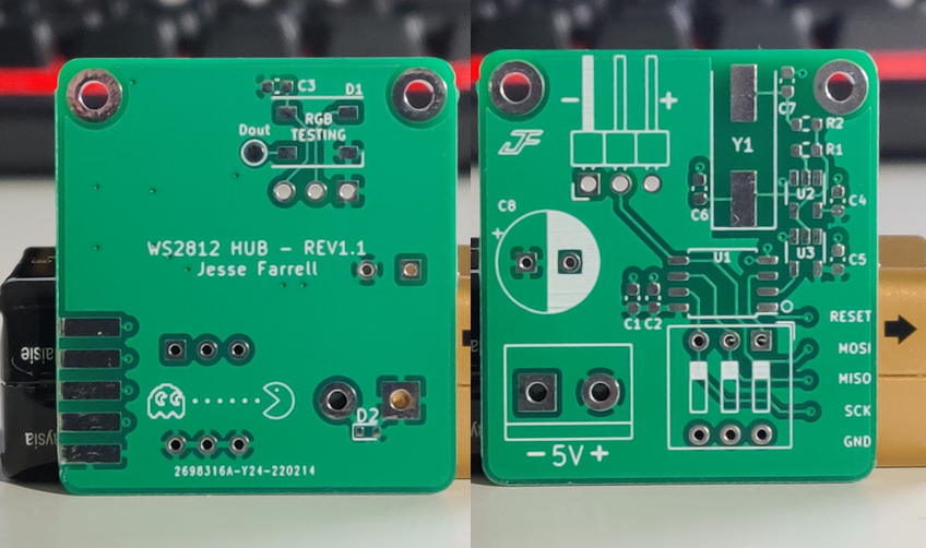
REV1.1 Board Update
01/30/2022 at 07:20 • 0 commentsAfter working with this board over the weekend there’s a couple changes, I’ve decided to make. Changes include:
- Added screw terminal for input power
- Added TVS diode at input
- Increased board outline
- Update silkscreens indicators
- Update MCU programming pads
![]()
Aside form these layout changes the project is sudo-complete, I just need to test this revision and create an enclosure in solidworks. Everythings tested and the firmware is good to go. I'll periodically update the files of this project over the coming week.
-
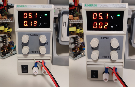
Power Requirments
01/30/2022 at 02:24 • 0 commentsTo determine the power requirements, I’ll turn a string of 5 led’s onto max brightness and monitor the input. At max brightness the recorded power consumption at 5V was about 950mW (190mA), and with all LEDs off its about 100mW (20mA). This corresponds to approximately 175mW (35mA) per LED. Note that these are just ballpark figures, with very questionable accuracy.
![]()
After getting a general idea of the power requirements I plugged a string of 100 WS2812s and recorded similar per LED power draw. I recorded 15.4W for 100 LEDs, so about 153mW per LED (adjusted for quiescent). For power supply recommendations I will go with the larger figure, 175mW per LED + 100mW.
![]()
I have a wall wart rated for 5V@3A, so I’ll be able to drive about 85 LEDs at max brightness (3A/0.035A). Of course, I don’t need to run these at max brightness, but I’d rather be safe than sorry. The final power supply recommendation is:
I= 0.035n + 0.02 [A] //5V supply current rating for 'n' LEDs
Just a final aside about the power planes on this board. I measured the power rails and its about 100mV pk-pk. I'm happy with this so I won't bother tweaking the bulk capacitance ect.
-
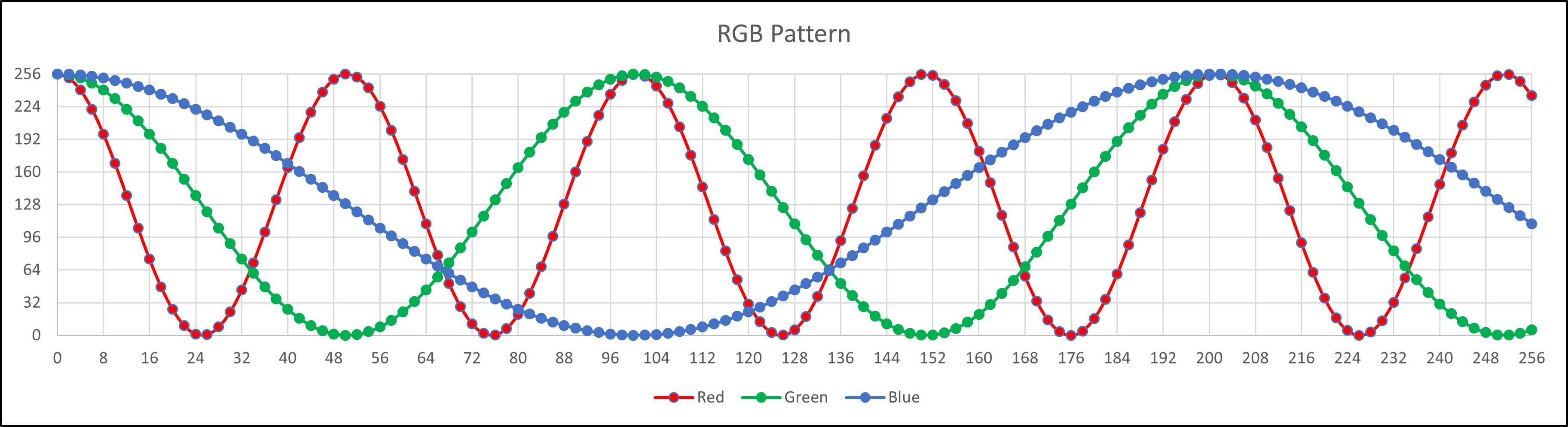
RGB Sweep
01/28/2022 at 06:14 • 0 commentsNow that I have a skeleton of the final program setup, I wanted to workout the kinks in the RGB strobing algorithm. Ideally, I would use cosine waves to slowly transitions between different colors; similar to what’s shown below.
![]()
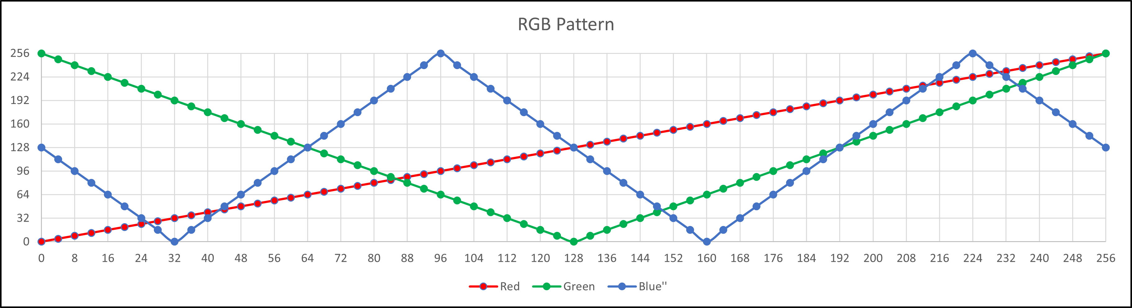
Alas, I forgot that MCU’s don’t really calculate trig functions, instead opting for look up tables. I don’t nearly have enough memory to accomplish this so I will use a linear version of this plot. I’ll add some variables to tweak the phase of the different signals.
![]()
I tried using the internal 8bit counter of this chip configured in CTC mode (Clear Timer on Compare match); however, the 8bit resolutions and frequency of this counter wasn’t very well suited for this function. The final linear implementation looks reasonable and can be tweaked by changing the RGB_SEED value. Here’s what it looks like with RGB_SEED_1 = 0x80d802. (Note that the seed value just changes the starting conditions of the different signals above)
The linear transitions definitely aren’t ideal, (see video), but its good enough for me.
-
WS2812B Protocol Testing w/ Attiny13a
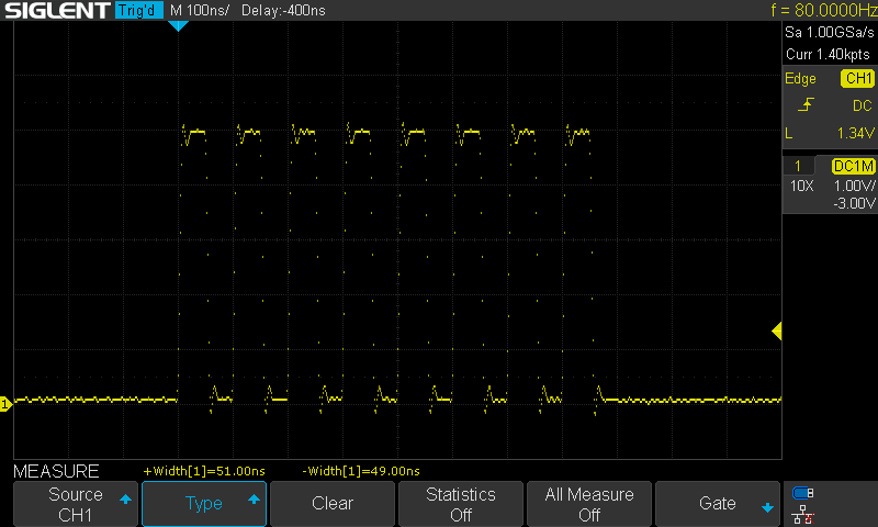
01/23/2022 at 19:29 • 0 commentsTo get started I wanted to understand what I’m working with. If I just toggle the pin, I’m able to get ~50ns pulse widths. This makes sense since our clock is 20MHz = 50ns period.
![]()
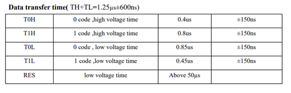
To extend the pulse widths I'll insert _asm(“nop”) commands. This is an assembly command telling the MCU to perform no operation. Assuming this instruction will only take 1 clock cycle (seems like pretty good assumption), I will need to pad the output toggle with around 7/8, and 15/16 to achieve the timings in the table below.
![]()
Here’s a hardcoded 0 using "nop" to configure the timings. The _asm(“nop”) instruction works as expected, and although it’s a bit wasteful its pretty handy.
![]()
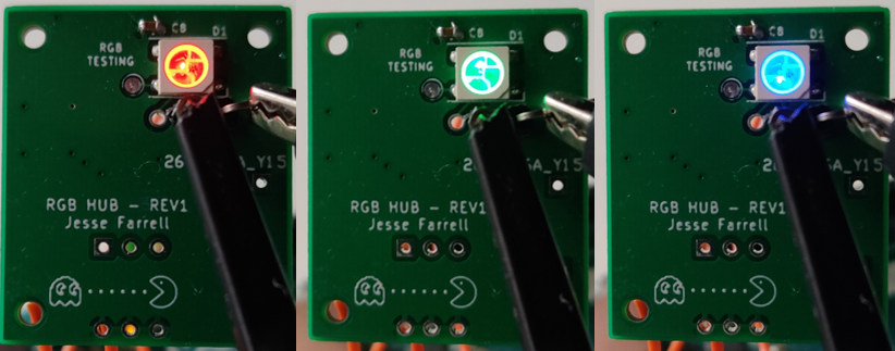
I moved the hardcoded 1/0 code into a function and called this function 24x to test a single WS2812B. With a bit of tweaking to account for delays entering and exiting the functions, the IC worked as expected. Here's a couple pictures of the different colors on the lowest brightness.
![]()
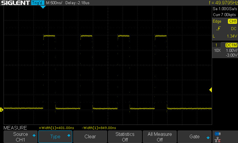
Testing the reset command, it looks like the IC follows its spec closely. It won’t reset below a 50us hold time. In this capture the signal was held low for approximately 50us but the LED did not update (cursors were likely a bit offset here). Increasing the delay to 55us and the IC worked as expected.
![]()
-
External Clock Validation
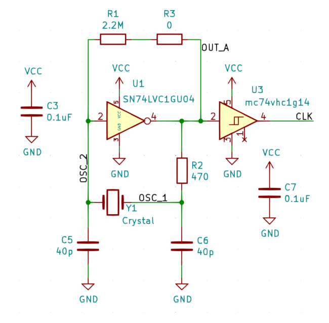
01/20/2022 at 23:46 • 0 commentsThe external clock for this widget is a Peirce Oscillator (shown in below). Calculations for component selection of C5/C6 and R2 are outlined in the project HAS. Note that R3 was added to allow for tweaking of the feedback resistor. Something I learned here is that a Schmitt trigger in place of U1 can cause the clock to intermittently fail. It sounds like this behaviour is caused by the uncertain thresholds off the Schmitt trigger. For example, for the MC74 IC the negative threshold @5V Vcc has a min threshold of 1.65V and a typical threshold of 2.9V.
![]()
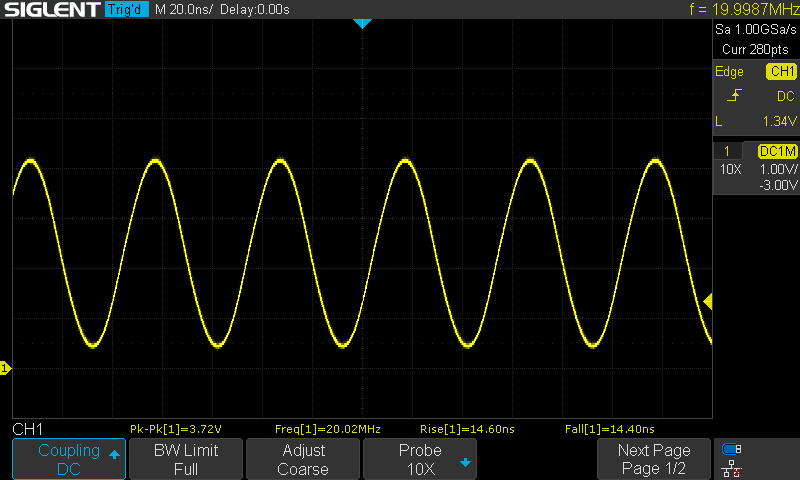
Here's a few scope captures of this circuit in operation. The signal OSC_2 going into pin 2 of U1 is a nice sinusoid seen below
![]()
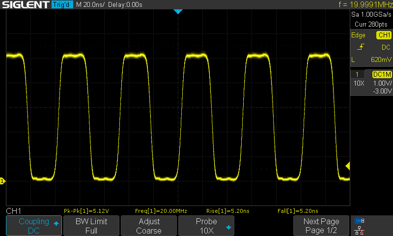
Here's the output of the first inverter; pin 4 of U1. As is, the clock is looking pretty clean, and would likely be fine to drive the Attiny.
![]()
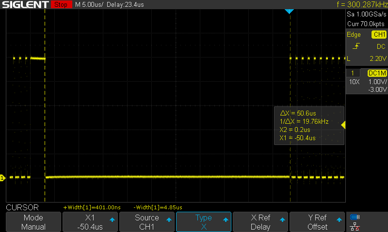
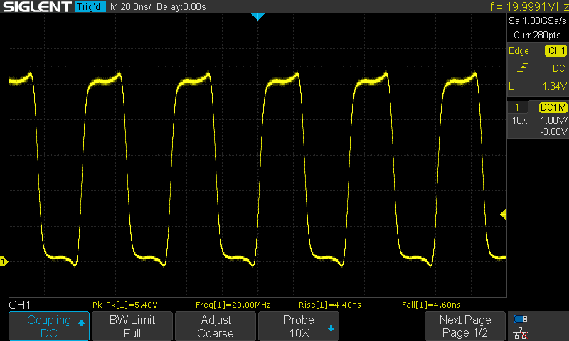
After the buffered inverter the clock edges are tightened up a bit more, but we’ve also introduced a bit of overshoot (There's a good chance my oscilloscope [1104X-E] is filtering the edges of this clock signal a bit). It might be a good idea to remove U3 to help reduce BOM cost.
![]()
-
Read Me
01/18/2022 at 20:51 • 0 commentsIn an effort to improve my documentation habits I'm going through my projects and pushing them to Hackaday. The main design process and calculations can be found in the project files labeled HAS (Hardware Architecture Specification).
These logs will be used as a dumping ground for validation results and firmware development.
*Currently working on validation/ firmware development*
WS2812 Controller
A cheap & cheerful widget to control those RGB strips everyone has