padnest
-
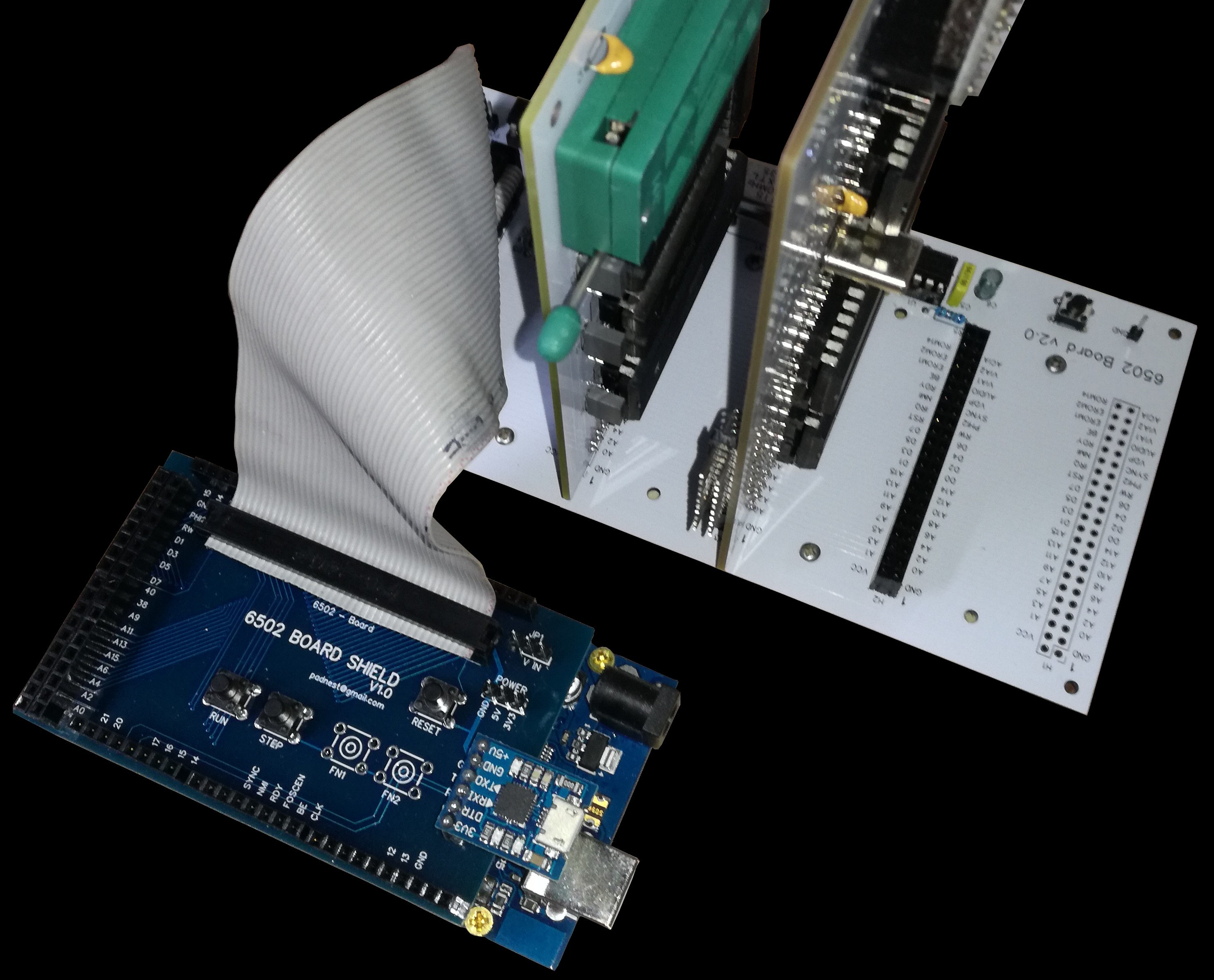
The Arduino Mega shield
02/14/2022 at 10:17 • 0 commentsI designed this shield to easily connect the Arduino Mega to the MRC6502 system.
![]()
It has pass through headers for bus signals, control buttons and a socket for an additional usb serial module.
![]()
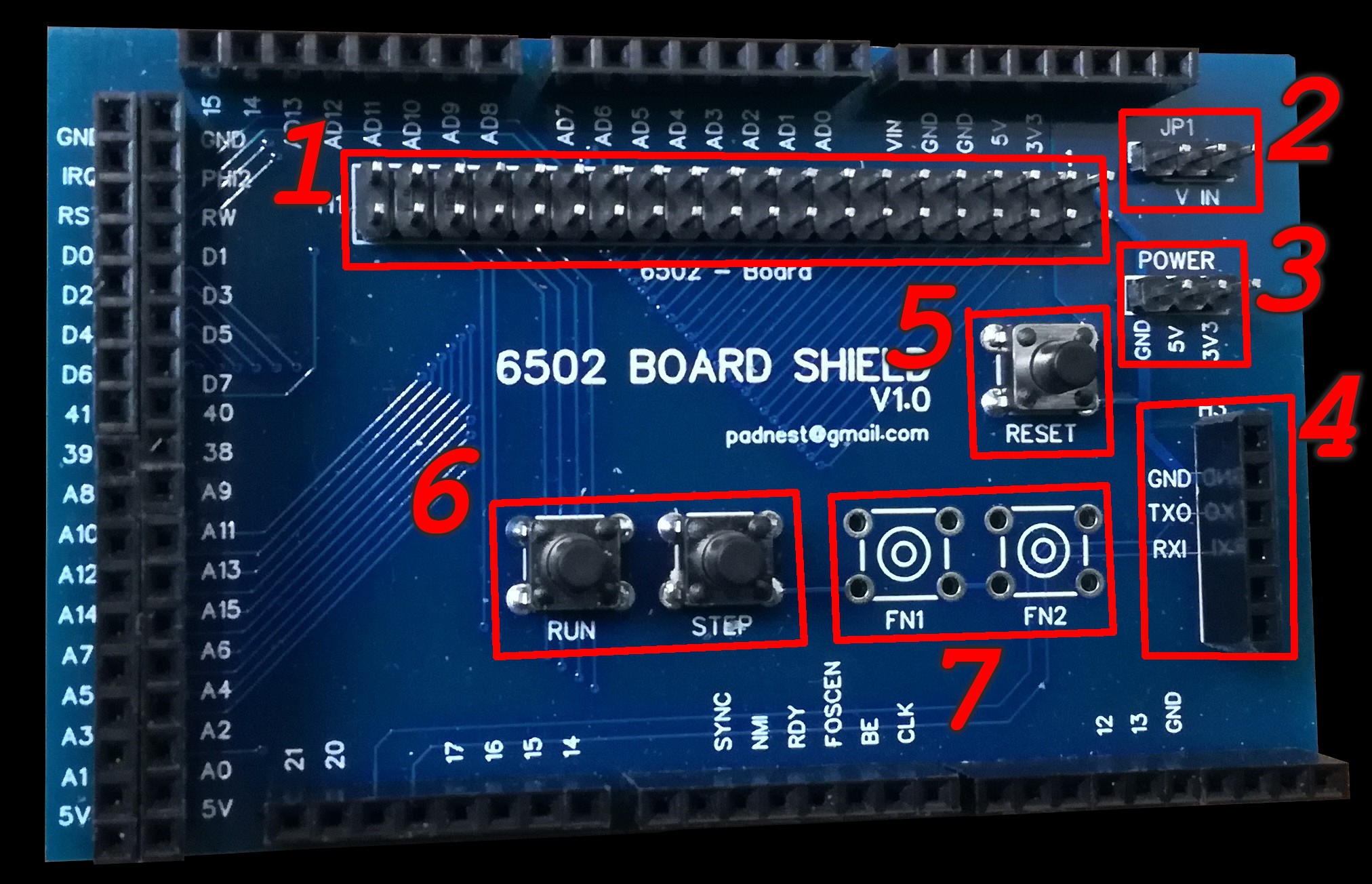
- 40 pin male header to connect the MRC6502 mother board (1)
- Arduino power supply selector (2)
- power rails header (3)
- CP-2102 usb serial module socket (4)
- reset button (5)
- CPU execution control buttons (6)
- extra function buttons (7)
Connections
Arduino can access to the system bus in order to control the CPU execution, read and write memory and devices registers, generate slow system clock or enable fast board clock generator.
![]()
Arduino used ports are:
- PORT L (bidirectional) ==> bus data lines
- PORT A (bidirectional) ==> low bus address lines
- PORT C (bidirectional) ==> high bus address lines
- PORT B:
- bit 0 (output) ==> bus IRQ line
- bit 1 (input) ==> bus PHI2 line
- bit 2 (output) ==> bus RST line
- bit 3 (output) ==> bus R/W control line
- PORT E:
- bit 3 (output) ==> mother board A-FOSCEN control line
- bit 4 (input) ==> bus SYNCH line
- bit 5 (output) ==> bus NMI line
- PORT H:
- bit 3 (output) ==> bus BE line
- bit 4 (output) ==> mother board A-CLK line
- PORT G:
- bit 5 (output) ==> bus RDY line
Schematics: here
See you next step.
Ciao!
-
The I/O board
02/09/2022 at 08:14 • 0 commentsA computer with no I/O capabilities doesn't do much... right?
So here we have the I/O board that will implement these interfaces:
- USB serial :: to communicate with a modern PC
- SPI (TTL) :: to experiment with any external SPI device like LCD display, sensors, real time clock, etc
- SD card :: the mass memory to read and write files
- GPIO user port :: for whatever else we want to connect
- P/S2 keyboard :: the primary input device
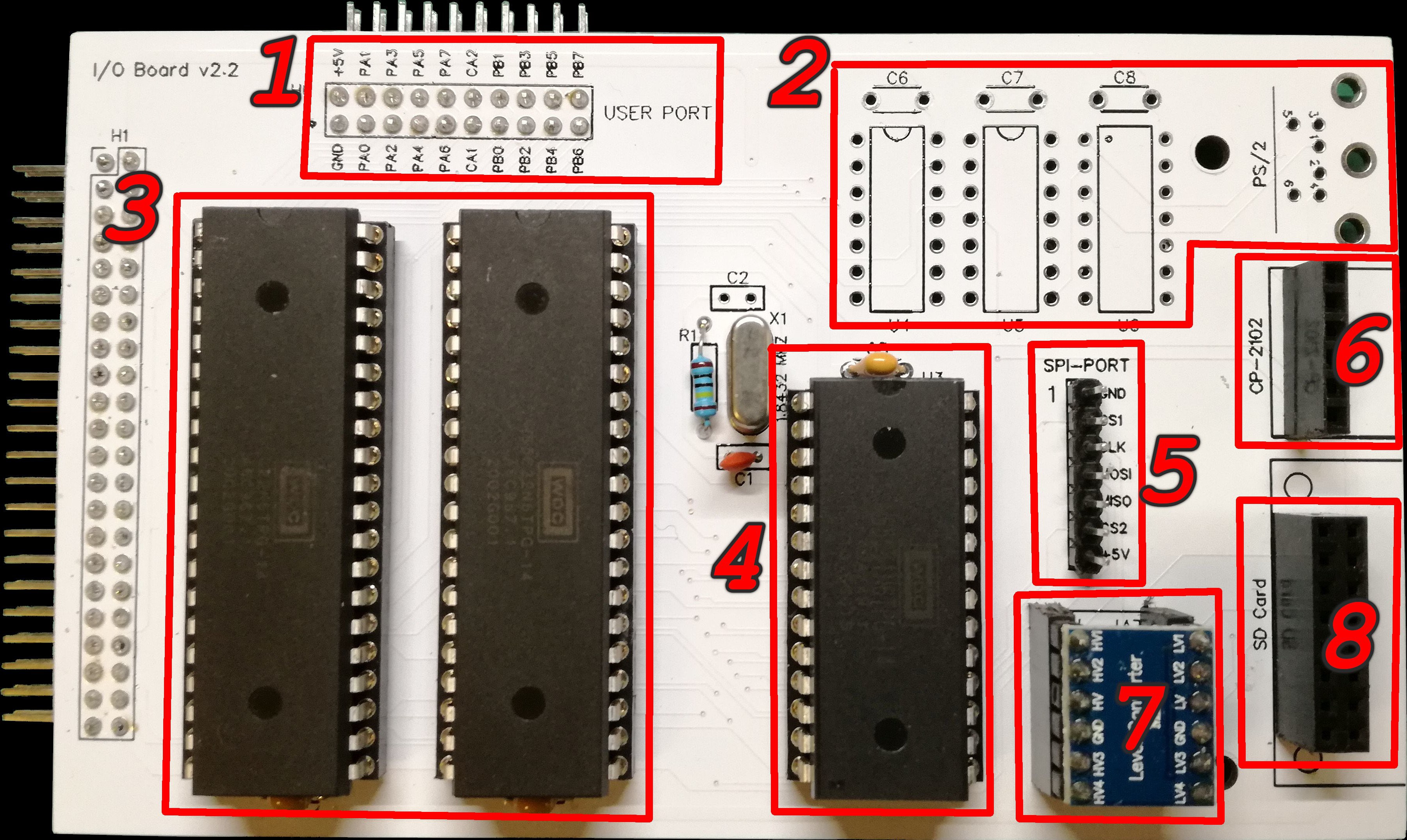
![]()
The I/O board has:
- User Port header for GPIO (1)
- PS2 keyboard adapter (2)
- two VIA W65C22N-14 for parallel and SPI comm (3)
- one ACIA W65C51N-14 for serial comm (4)
- SPI port header supporting two general TTL devices (5)
- CP-2102 module socket for USB serial (6)
- SD levels adapter module (7)
- SD card module socket (8)
Schematics: here
User port (1)
It is a GPIO port directly connected to the peripheral data ports of VIA#1.
This port also provides the system power supply (+5v).
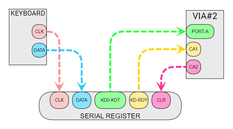
PS/2 keyboard adapter (2)
Is the logic needed to adapt a standard PS/2 keyboard protocol to the VIA#2.
![]()
The PS/2 keyboard clock and data lines go into an external serial register (74LS164) that feeds VIA#2 with:
- KD0-KD7 ==> the keyboard data byte received (8 bits)
- KD-RDY ==> the keyboard data byte ready signal (when a complete data byte is received)
VIA#2 CA1 is configured as input to fire an CPU IRQ when keyboard data byte has been received and can be processed.
VIA#2 CA2 is configured as output to clean the serial register in order to receive the next keyboard data event.
Perhaps it will also be necessary to add a protection between the logic and the VIA#2 port.
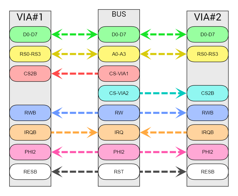
VIAs (3)
Two WDC Versatile Interface Adapters W65C22N (datasheet) are connected to the system bus in this way:
![]()
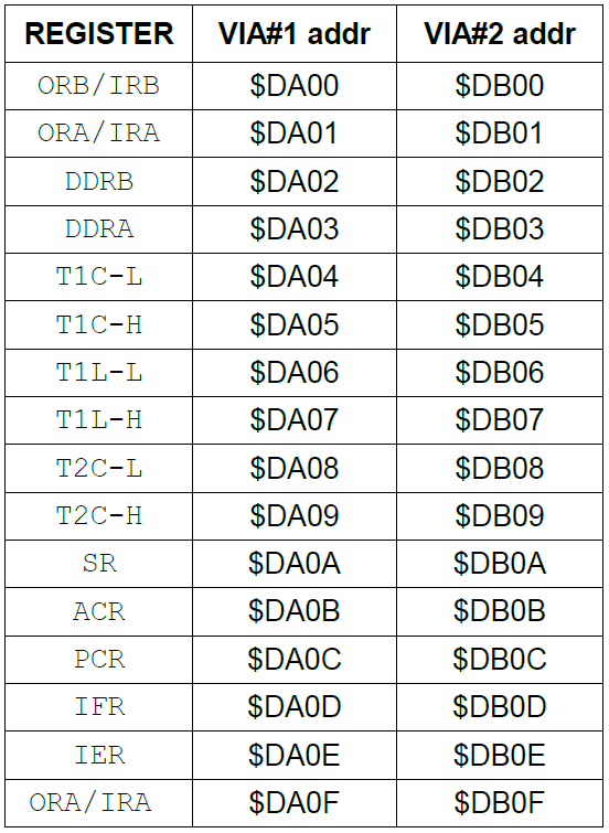
Each VIA has 15 internal registers that can be accessed by address llines A0-A3.
The base address is $DA00 for VIA#1 and $DB00 for VIA#2 and the memory mapping will be:
![]()
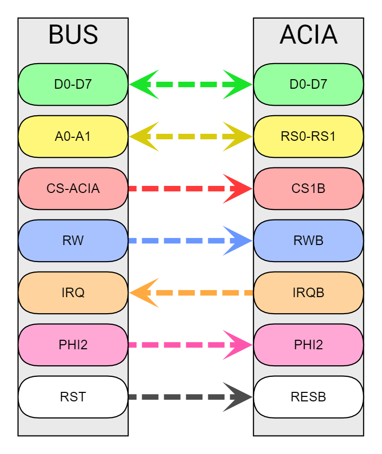
ACIA (4)
The WDC Asynchronous Communications Interface Adapter W65C51N (datasheet) is connected to the bus in the same way but it has only 4 internal registers so just two address lines, A0-A1, are used:
![]()
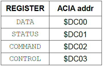
The ACIA base address is $DC00 and the memory mapping of internal registers will be:
![]()
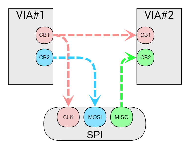
SPI port and SD card module (5 & 8)
The SPI protocol is hardware implemented using the serial registers of the two VIAs: this allows us to have the maximum possible data transmission speed!
![]()
CB1 is configured as serial clock output on VIA#1 and as serial clock input on VIA#2.
CB2 is configured as serial data output (MOSI) on VIA#1 and as serial data input (MISO) on VIA#2.
Perhaps it will also be necessary to add a protection between VIA#1 CB1 and VIA#2 CB1.
SPI is shared between the SPI Port and the SD Card module; the SPI port has two dedicated CS lines connected to VIA#2 PB5 and PB6
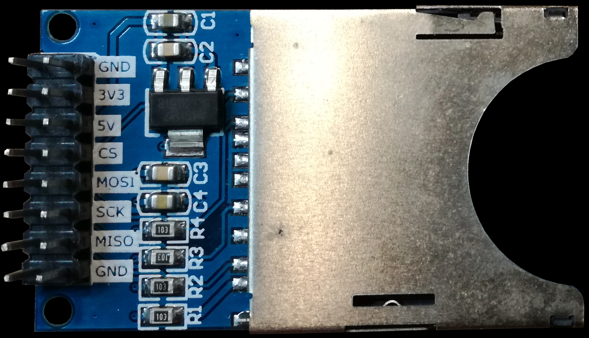
Here the popular Arduino SD Card module that I have choosen:
![]()
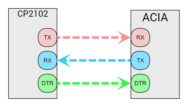
Usb serial (6)
The usb serial interface is provided by a CP-2102 usb serial module and is connected to the ACIA:
![]()
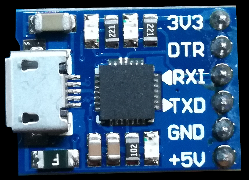
Here the CP-2102 usb serial module I'm using:
![]()
Stay tuned for the next step!
Ciao!
-
The MRC6502 development tools
02/05/2022 at 16:08 • 0 commentsTo develop on MRC6502 I will use:
- Visual Studio Code
- Kick Assembler
- Arduino IDE :: for Arduino sketch programming and serial IO to the MRC6502 system
- Phyton + Transduino.py :: to program MRC6502 RAM via Arduino
- WinCUPL :: to compile PLD configuration
- TL866II plus + Xgpro/XGecu :: to program the PLD and the EEPROM
Setup
- download and install Visual Studio Code
- download and extract Kick Assembler
- download and install OpenJdk Java 11
- download and install Arduino IDE
- download and install WinCUPL
- download and install Xgpro/XGecu
Visual Studio Code configuration
- Switch to Extension view (CTRL+SHIFT+X)
- write 'kick assembler' in the search text box and install 'Kick Assembler 8-Bit Retro Studio' by Paul Hocker
- open the settings (CTRL+,) ; write 'kick' in the search text box and in User tab set:
- Kickassembler › Assembler: Jar ==> full path to the kick assembler jar file
- Kickassembler › Assembler: Main ==> kickass.KickAssembler
- Kickassembler › Assembler › Option: Output Directory ==> bin
- Kickassembler › Assembler › Option: Source Symbols ==> checked
- Kickassembler › Java: Runtime => full path to openjdk java executable file (usually in bin subdirectory)
- Kickassembler › Opcodes: 65c02 ==> checked
- open the keyboard shorcuts (CTRL+K CTRL+S); write 'kick' in the search text box and:
- assign 'F6' for 'Kick Assembler: Build'
- assign 'SHITF + F6' for 'Kick Assembler: Build and Debug'
- assign 'SHITF + F5' for 'Kick Assembler: Build and Debug Startup'
- assign 'F5' for 'Kick Assembler: Build and Run'
- assign 'CTRL + F5' for 'Kick Assembler: Build and Run Startup'
- assign 'CTRL + F6' for 'Kick Assembler: Build Startup'
Ciao!
-
Timings #1 - CPU vs RAM&ROM
01/29/2022 at 07:51 • 0 commentsTimings are crucial! Let's check if we can go with a 4MHz clock using 70nS SRAM and the EEPROM.
CPU timings
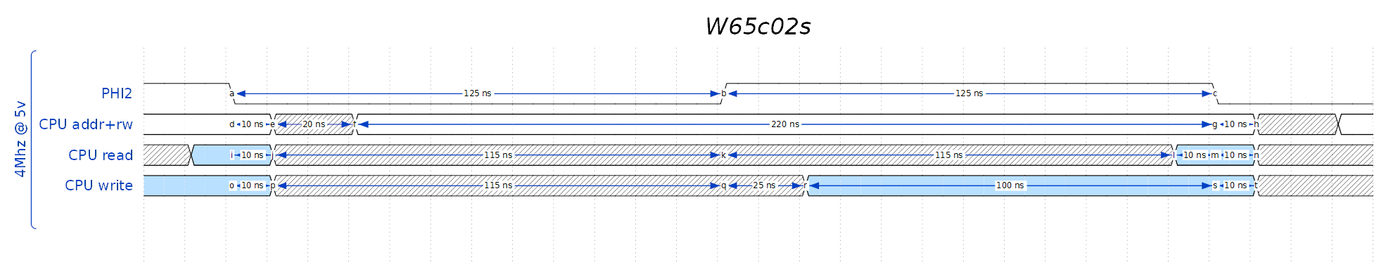
First of all I want to try to recap CPU informations about timings from the WDC W65c02s datasheet.
In the picture:
- PHI2: at 4MHz clock speed each PHI2 phase lasts 125nS for a total time of 250nS.
- CPU addr+rw: setup time for A0-A15 and RW signals is 20nS; this happens after 10nS from the PHI2 HIGH-to-LOW transition.
- CPU read: data acquisition happens after 115nS from PHI2 LOW-to-HIGH transition and it lasts 20nS.
- CPU write: data exposure begins after 25nS from PHI2 LOW-to-HIGH transition and it lasts 110nS.
![]()
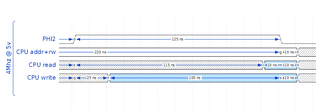
Let's zoom now into PHI2 HIGH phase:
![]()
It's very important to observe what happens after the PHI2 HIGH-to-LOW transition:
- CPU read: the CPU requires no data changes for 10ns.
- CPU write: the CPU holds data stable for 10ns.
PLD delay
PLD, as you already know now, handles all the glue logic; there is a propagation delay introduced by the ATF22V10C-15 (max 15nS) but this should have no practical effects on timings.
RAM timings
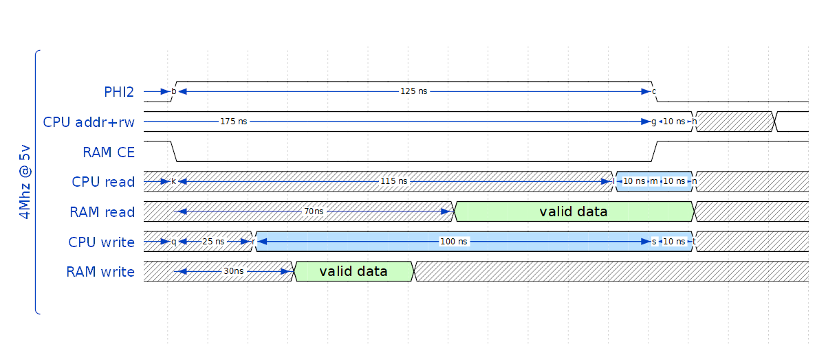
In the next picture:
- RAM CE: PLD select the RAM (CE goes LOW) when the address matches and PHI2 goes HIGH; this will result in a (almost ***) perfect match.
- RAM read: RAM presents stable data after 70nS from selection (CE goes LOW) .
- RAM write: RAM requires to have stable data after 30nS from selection (CE goes LOW) .
![]()
(almost ***): can we have problems when RAM CE goes HIGH but CPU is still reading for additional 10nS?
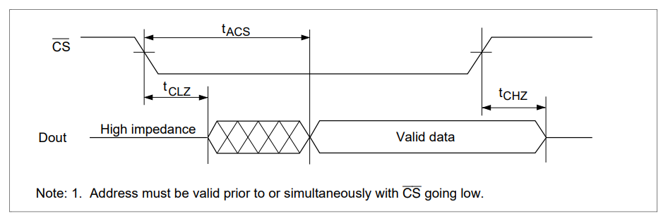
From RAM datasheet:
![]()
When CS goes HIGH the RAM hold valid data for tCHZ time that should be from 0nS to 25nS so we need to test RAM access @4Mhz to verify if this is true and if it can be a real or a pratical problem.
Perhaps the PLD propagation delay (15uS) could save us here, I don't know... (tests are required).
EEPROM timings
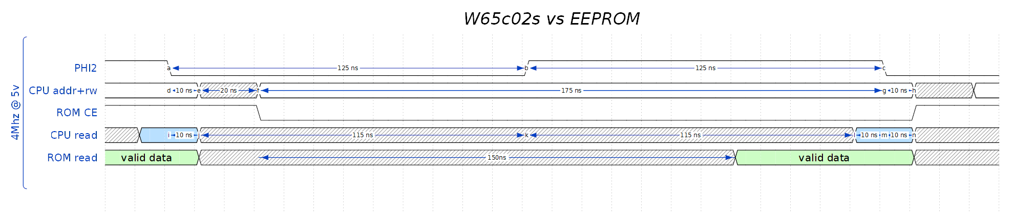
Let's check now the AT28C256-15 EEPROM:
- ROM CE: PLD select the ROM (CE goes LOW) when the address matches (without considering PHI2).
- ROM read: ROM presents stable data after 150nS from selection (CE goes LOW) .
![]()
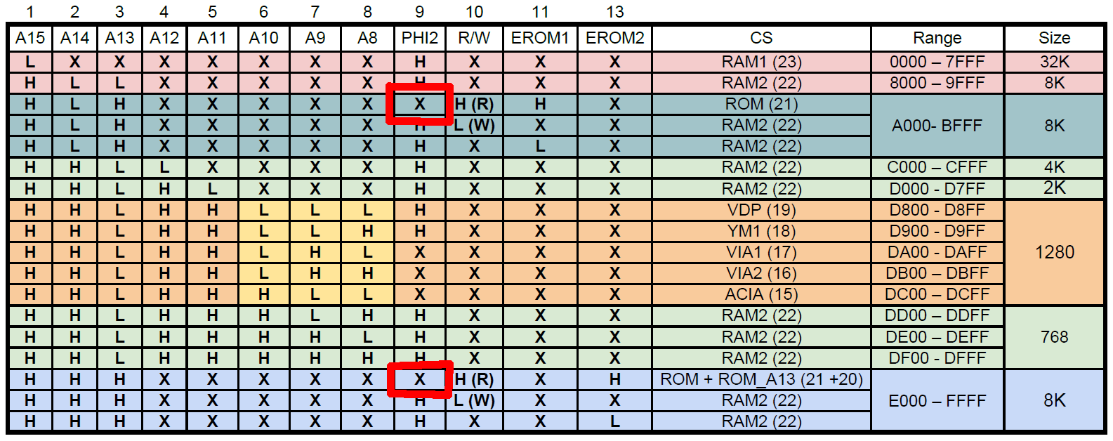
I have to update the PLD glue logic table applying the changes in red:
![]()
Next step: RAM/ROM test on access
Let me know what do you think in the comments...
Ciao!
PS:
I would like to thank everyone who sent join requests for the project. I'm considering whether or not to accept some collaborations maybe a little further on. Commenting on posts is already a way to collaborate and to help me. Many many thanks!
-
The (not only) CPU board
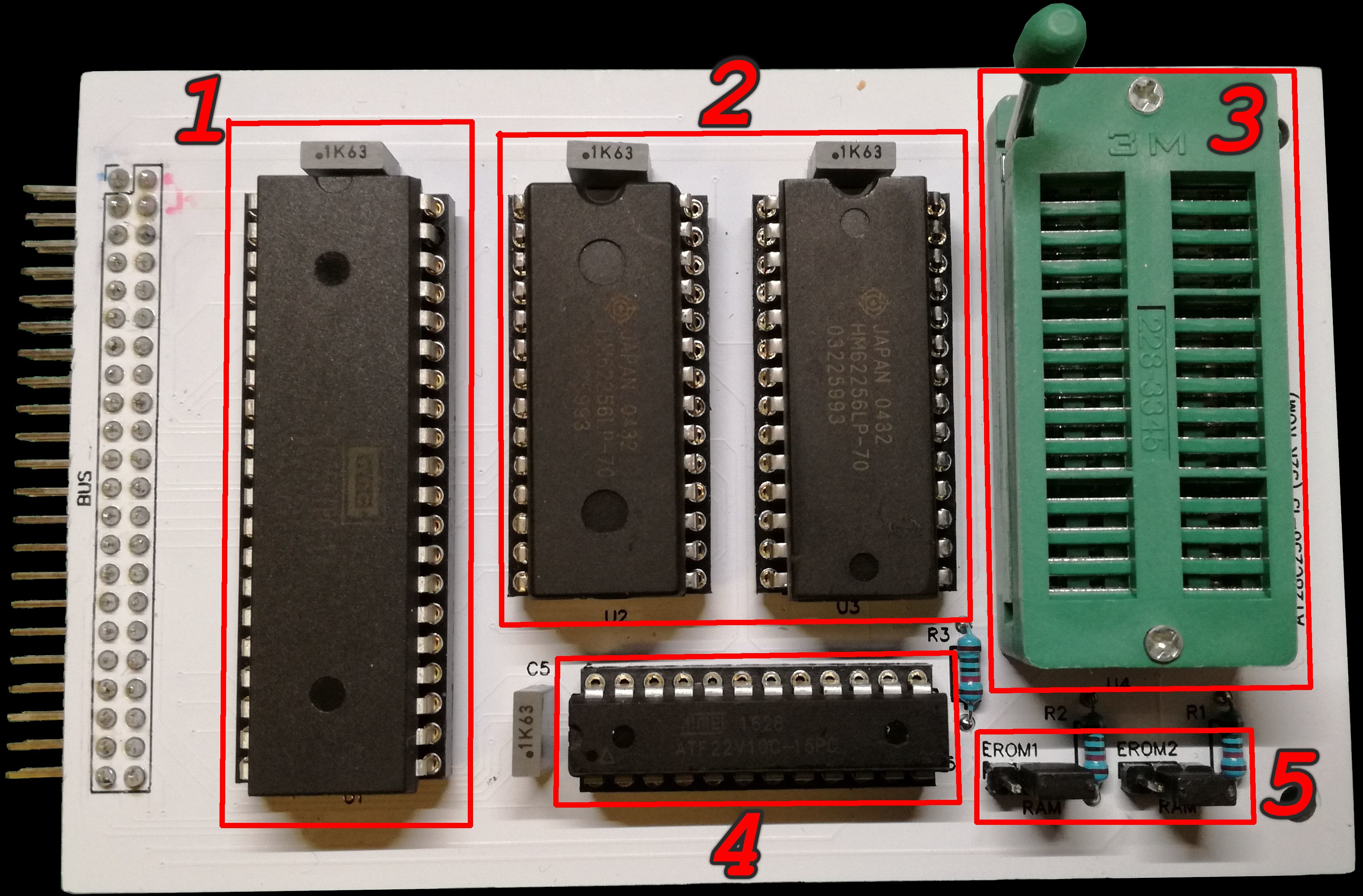
01/28/2022 at 14:48 • 0 commentsThe CPU board hosts:
- the CPU (1)
- the RAM (2)
- the (EEP)ROM (3)
- the PLD (4)
- jumpers to configure memory mapping (5)
![]()
In this board prototype I forgot to add a jumper in order to manually select the ROM banking (RAM14).
![]()
I will add another jumper for this scope in the next revision.
Schematics: here
---------- more ----------CPU (1)
The CPU is the WDC W65c02s processor and it has many improvements against the old MOS 6502:
- full static core (we can stop the clock in LOW or HIGH state without losing the internal state)
- 70 instructions (56 on MOS 6502)
- 16 addressing modes (13 on MOS 6502)
- max 14 Mhz clock (2 Mhz on MOS 6502)
- supply voltage from 1.8 to 5 volts
- low power consumption
Datasheet: here
RAM (2)
64Kb of static RAM are provided by two HM62256LP-70.
Datasheet: here
ROM (3)
A ZIF socket to host the 32Kb AT28C256 EEPROM.
Datasheet: here
PLD (4)
All the system 'glue logic' is managed by an ATmel ATF22V10C-15.
Datasheet: here
Memory configuration (5)
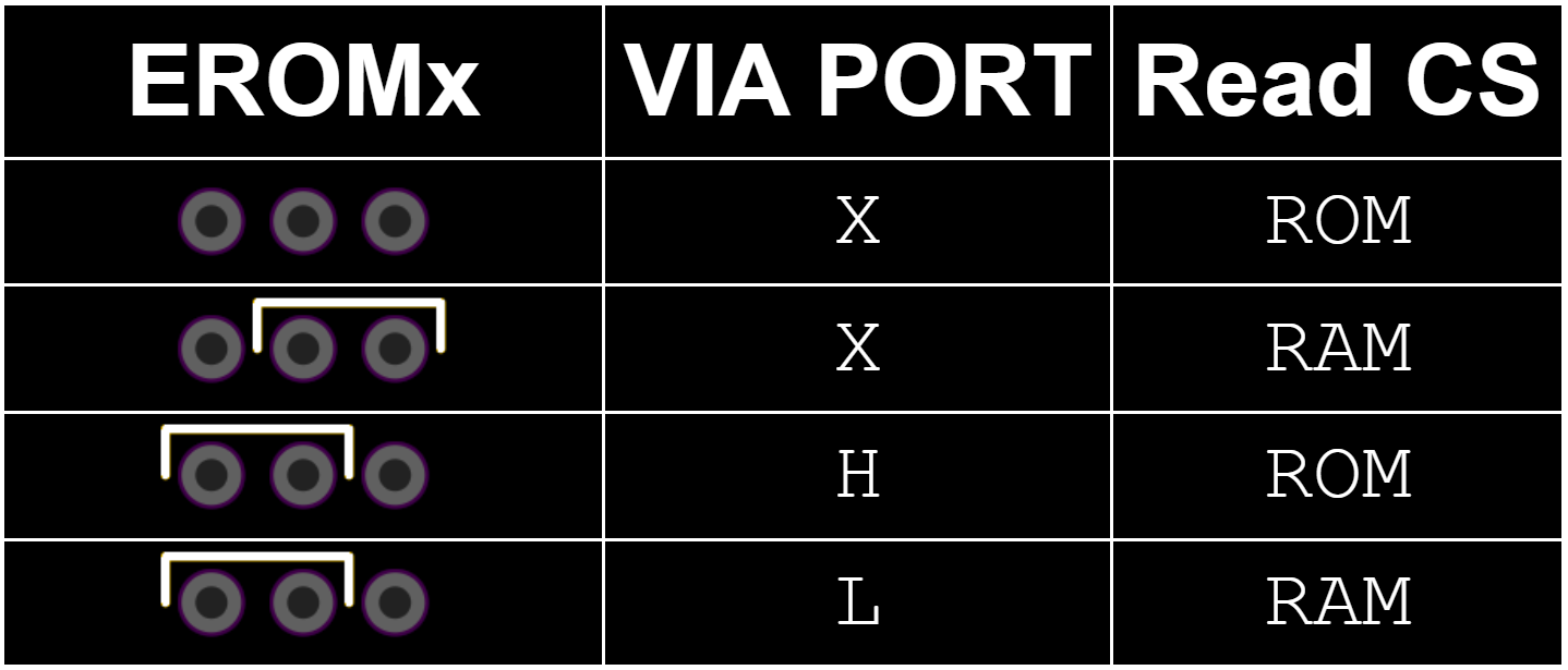
The jumpers can be used to control what to read at address ranges A000-BFFF (EROM1) and E000-FFFF (EROM2).
You can exclude and override the respective EROMx signals generated by one of the VIA (that can be programmatically used to control the configuration).
![]()
Ciao!
-
The memory map
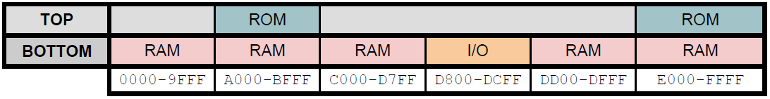
01/24/2022 at 11:25 • 0 commentsI designed the system memory mapping with these purposes in mind:
- to have 64Kb of RAM in the bottom layer
- to have 16Kb of ROM in the top layer
- to have the possibility of banking out the ROM having access to the background RAM
- any write operation on ROM is always addressed to the background RAM
- do not waste RAM mapping I/O devices
Memory layers:
![]()
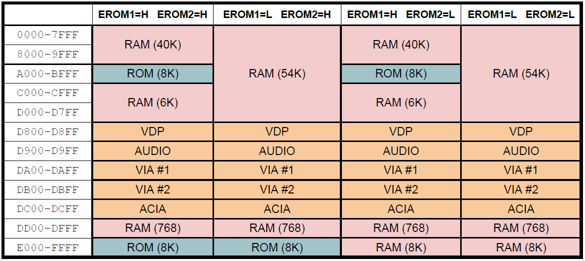
Memory configurations
Bus lines EROM1 and EROM2 are used to enable or disable ROM layers: disabling the ROM you can read from the background RAM.
These lines can be programmatically controlled by one of the VIAs port.
![]()
Each I/O device has 256 memory locations (one page) of space to map internal registers.
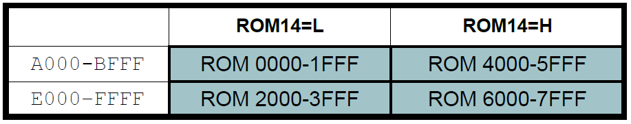
---------- more ----------ROM banking
Since the ROM size is 32Kb we can have four 8Kb banks and so two different versions of ROM.
Bus line ROM14 is used to select which ROM locations are visible at the assigned ROM spaces.
Also ROM14 can be programmatically controlled by one of the VIA port (this might be a bit tricky to do at runtime!).
![]()
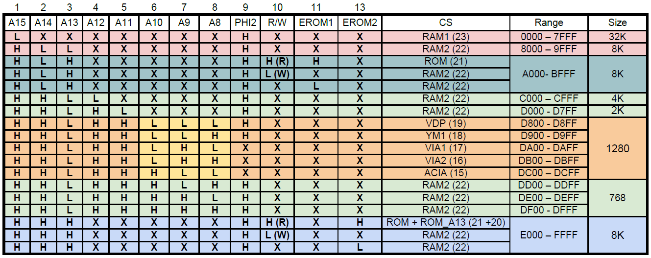
Glue logic
To implement all the chips selection logic just a single IC will be used: a programmable logic device (PLD).
This choise has many advantages (reduced number of components, easy to make changes, space optimization).
The PLD (an Atmel ATF22V10C) will be programmed following this table:
![]()
Inputs signals:
- A15 to A8: address lines
- PHI2: system clock used to match the RAM/ROM timings
- R/W: read/write line used to select background RAM on write
- EROM1, EROM2: ROM enabled lines
Output signals:
- 15 to 23: used to select the respective device (LOW level)
Next step: CPU board.
Ciao!
-
The motherboard
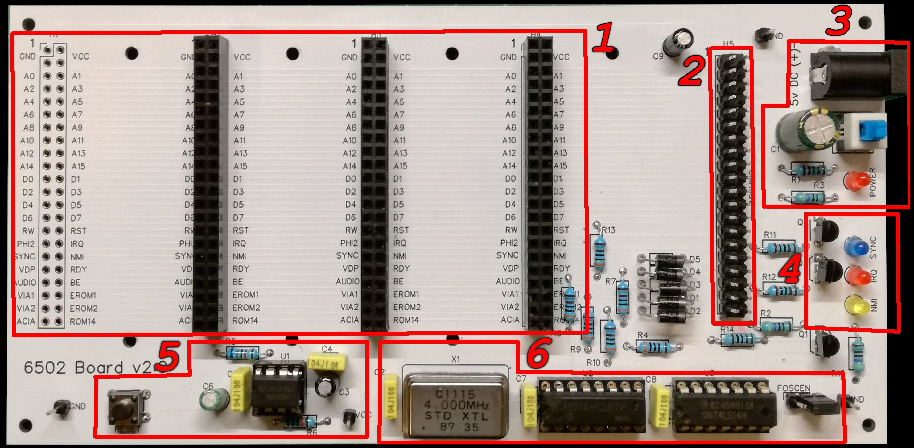
01/21/2022 at 07:59 • 0 commentsThis is essentially the board that houses the other boards (modules) and provides some basic functionalities as system clock, arduino control, power-up reset, etc.
The motherboard has:
- four 2x22 pins bus connectors (1)
- one 2x20 pins arduino connector (2)
- the power supply plug (DC 5v - 3000mA), switch and led (3)
- some leds to show SYNCH, IRQ and NMI lines status (4)
- the power-up reset logic and the reset button (5)
- the system clock switcher and the fast clock generator (4Mhz) (6)
![]()
NOTE: this is still a prototype... I may have to change something if necessary.
A bus socket is unpopulated (for now) to easily connect the probes.
Schematics: here
---------- more ----------Bus connectors (1)
All bus connectors are identical so child boards can be installed in any place.
The bus has the following signals:
- address (A0 - A15)
- data (D0 - D7)
- control (RW, RDY, BE, SYNCH)
- interrupt (IRQ, NMI)
- system clock (PHI2)
- rom banking (EROM1, EROM2, ROM14)
- device selection (VDP, AUDIO, VIA1, VIA2, ACIA)
- 5v power supply (VCC)
- ground (GND)
Arduino connector (2)
An Arduino MEGA can be connected for developing and debugging purposes:
- system clock control (slow mode)
- CPU operations detection and trace
- runtime address breakpoints handling (add, remove on the fly)
- CPU code execution stepping
- direct memory read and write (DMA)
- direct software programming (without the need to remove the ROM every time)
Power supply (3)
A DC 5v regulated power supply must be use. A 3000mA of max current ouput should be fine.
Power-up reset (5)
When switched on the 555 timer, configured in Monostable mode, keeps down the reset line for about 750 milliseconds. The same time is guaranteed when the reset button is pressed.
System clock (6)
A 4Mhz oscillator module provides the (fast) system clock.
Arduino can takes the control (A-FOSCEN signal) of system clock generation (A-CLK signal) in order to stepping CPU execution, access to memory or devices, running at slow rate, etc.
Next step: memory mapping.
Ciao!
-
Welcome to the project
01/19/2022 at 17:05 • 0 commentsHi and thank you for following my project! I will try to post at least one update per week... stay tuned and please support this project!
Comments and suggestions are very welcome!!!
Next Step?
The motherboard details.
Ciao!
MRC6502 - Modular Retro Computer
MRC6502 is a fantastic opportunity to learn more about digital electronics and 6502 assembly programming... step by step.