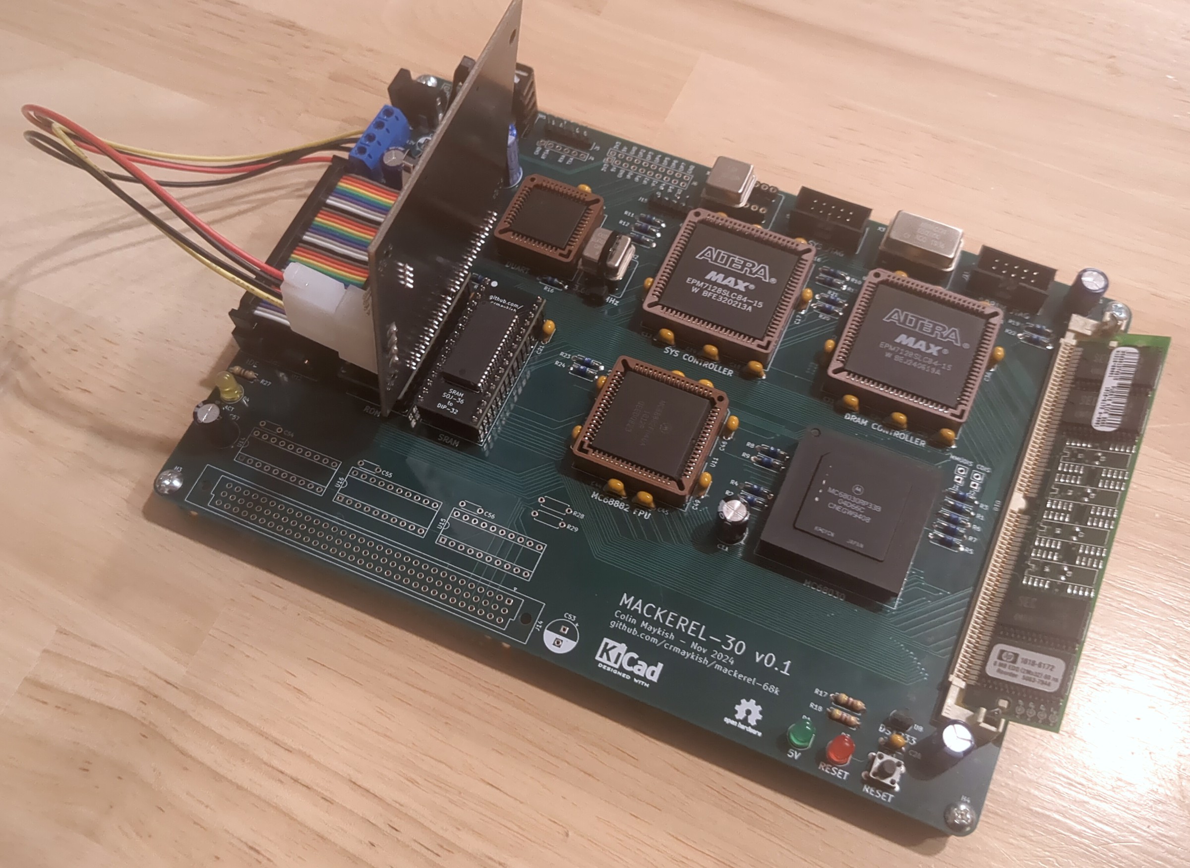
-
128MB Ought To Be Enough For Anybody
01/04/2025 at 17:59 • 4 commentsI was a bit premature in declaring the DRAM controller for Mackerel-30 complete. It was minimally functional as an 8-bit wide memory, but failed for any multi-byte or offset bus cycles. Implementing these wider memory cycles correctly requires some additional logic in the controller to correctly select the CAS lines for all possible bus cycle types.
On 72-pin SIMMs, there are four RAS lines and four CAS lines. Asserting a pair of RAS lines (0,2 or 1,3) selects between the two "sides" of the SIMM in the case of double-sided SIMMs (Note: these sides refer to how the DRAM chips are wired electrically, not necessarily how they are physically soldered to the PCB). Each of the CAS lines acts like a byte-select pin for the four bytes in the 32-bit wide SIMM. The trick to getting the correct bytes from DRAM onto the data bus requires decoding the SIZ0, SIZ1, A0, and A1 pins from the CPU into the right combination of CAS signals for the SIMM.
![]()
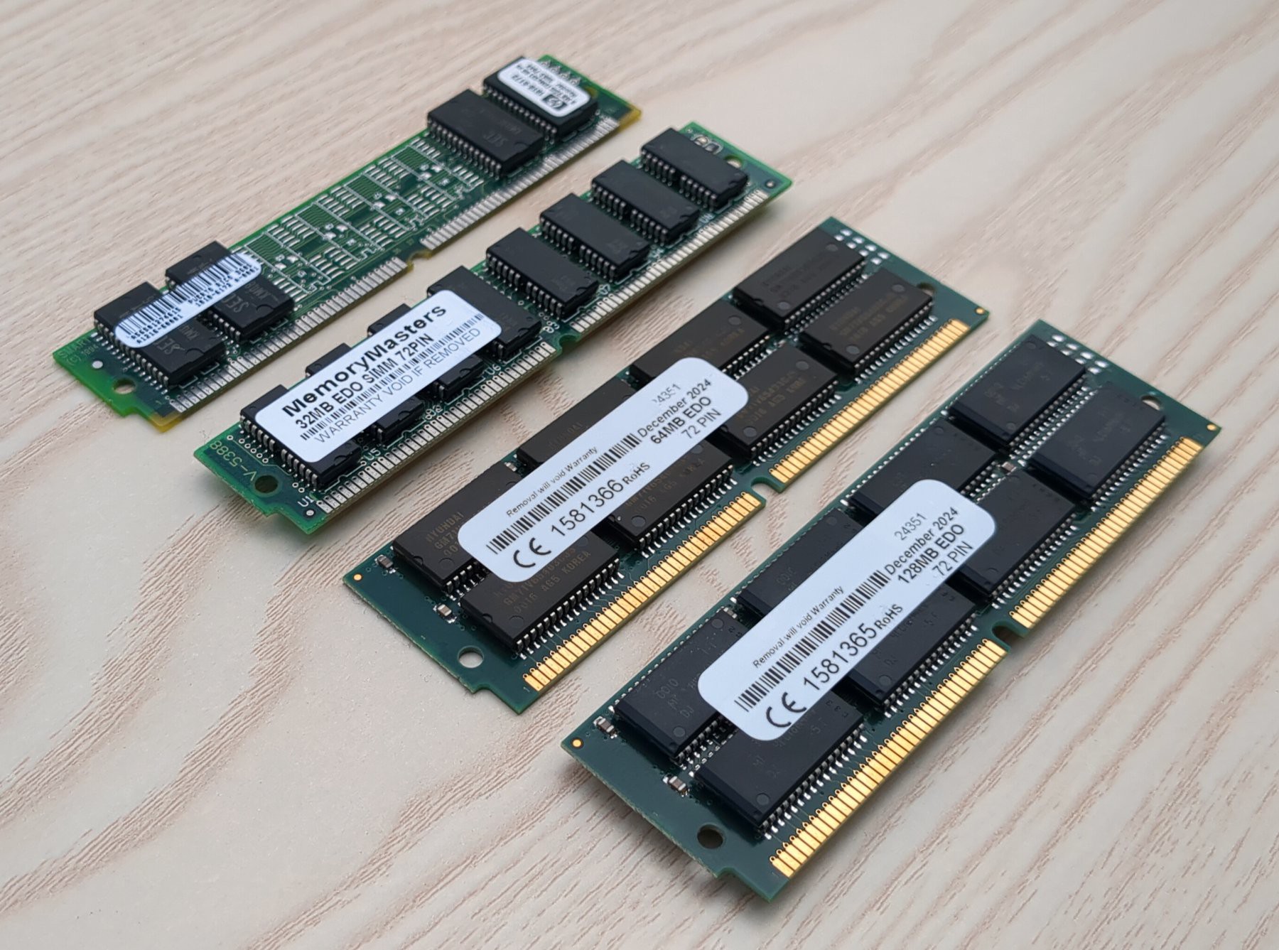
Top to bottom: 8 MB, 32 MB, 64 MB, and 128 MB SIMMs. The 64 MB SIMM is electrically single-sided (i.e. one-rank), the others are all electrically double-sided (i.e. two-rank). Fortunately, the MC68030 datasheet covers all of this in detail.
![]()
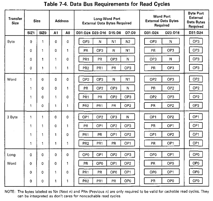
These two tables show how the SIZ0 and SIZ1 pins can be used to determine the requested bus width and how the A0 and A1 pins are used to set an offset if the request is not long word-aligned.
![]()
This huge table displays all possible combinations of bus width and offset and shows where the data is expected to be in each case. Since the DRAM always acts as a 32-bit wide memory, each of the entries in the Long-Word Port column map to a combination of CAS lines. For example, if the CPU requests a 16-bit word with an offset of 1 (row 6), the second and third bytes of the DRAM need to be read, so the CAS pattern is 0110 (active high).
The easiest way to translate this information into Verilog for the DRAM controller is with a case statement:
wire [3:0] CYCLE_TYPE = {SIZ1, SIZ0, ADDR[1], ADDR[0]};
reg [3:0] CAS;    // active high

always @(*) begin
    case (CYCLE_TYPE)
        // CYCLE TYPE <= CAS[3:0]

        // byte
        4'b0100: CAS <= 4'b1000;
        4'b0101: CAS <= 4'b0100;
        4'b0110: CAS <= 4'b0010;
        4'b0111: CAS <= 4'b0001;

        // word
        4'b1000: CAS <= 4'b1100;
        4'b1001: CAS <= 4'b0110;
        4'b1010: CAS <= 4'b0011;
        4'b1011: CAS <= 4'b0001;

        // 3-byte
        4'b1100: CAS <= 4'b1110;
        4'b1101: CAS <= 4'b0111;
        4'b1110: CAS <= 4'b0011;
        4'b1111: CAS <= 4'b0001;

        // long word
        4'b0000: CAS <= 4'b1111;
        4'b0001: CAS <= 4'b0111;
        4'b0010: CAS <= 4'b0011;
        4'b0011: CAS <= 4'b0001;

        default: CAS <= 4'b1111;
    endcase
end
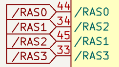
One issue I ran into while putting this solution together was strange RAS behavior. Each pair of RAS lines is supposed to act as a bank selector, but when I implemented this, I lost access to half the bytes in the memory. It turns out I mislabeled the RAS pins on the SIMM slot in my schematic and had RAS1 and RAS2 swapped. Fortunately, this is all semantics and swapping RAS1 and RAS2 in the CPLD pin mapping solved this problem entirely.
![]()
Can you spot the problem? With the DRAM now handling different cycle types correctly, I set up address decoding to handle 64 or 128 MB SIMMs. The SIMM bank is selected based on the A26 line. If A26 is 0, RAS0 and RAS2 will be asserted, if A26 is 1, RAS1 and RAS3 will be asserted instead. This allows support for either a 64 or 128 MB SIMM, only the addressable size of the DRAM will change: 0x4000000 or 0x8000000 respectively. Smaller single-sided SIMMs (4 and 16 MB) should also work without modification, but other sizes of double-sided SIMMs would require modification to this address decoding scheme to be fully mapped, but who doesn't want as much RAM as possible anyway!?
![]()
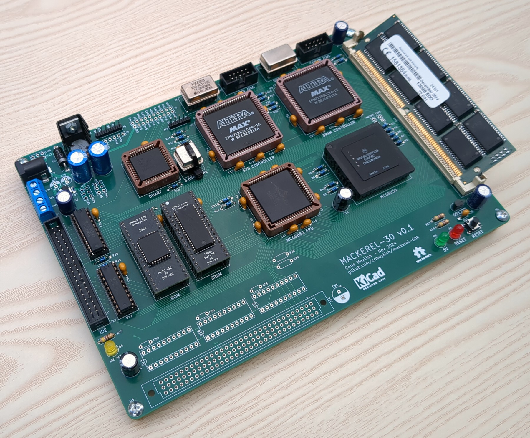
Mackerel-30 with 128 MB SIMM installed To wrap up this DRAM improvement, I revamped the memory test code in the bootloader. There are now two ways to test memory: a simple 8-bit read and write test and a new 32-bit test that can cover the entire 128 MB memory space. The 32-bit test takes a start address and a size and writes the 32-bit address value to the memory at that same address, e.g. it will write the long-word 0xC0000000 to the memory at address 0xC0000000. This not only tests that the read and write is working for 32-bit cycles, but it makes it easy to check for incorrect or duplicate mapping across a whole range of memory. Each long-word of DRAM should contain its own address as its value at the end of the test. Running this test with the 128 MB SIMM installed shows that the entire memory space is accessible and uniquely mapped.
Does Mackerel-30 actually need 128 MB of RAM? Probably not, but I'm pretty happy that it's working all the same.
Verilog implementation of the DRAM controller: https://github.com/crmaykish/mackerel-68k/blob/master/pld/mackerel-30/dram_controller/dram_controller.v
-
More Mackerel-30 Bringup Progress
12/15/2024 at 00:27 • 0 comments![]()
Current state of the Mackerel-30 prototype board Mackerel-30 board bringup is going well for the most part. I've got the IDE interface and DRAM controller hooked up and functional. I did make a mistake in IDE wiring though. One of the buffer chips between the IDE interface and the CPU data bus has the bits wired in reverse order, i.e. bits 0-7 are mapped to 7-0. Fortunately, the rest of the control circuitry is wired correctly and the bits can be reversed in software for now. This adds a bit of overhead, but Mackerel-30 is not winning any speed contests right now anyway. I'll add it to the list of fixes for the next PCB revision.
I also ported over my DRAM controller from Mackerel-10. Going from four 30-pin SIMMs to a single 72-pin SIMM required a bit of adjustment to the CAS and RAS logic, but the state machine and refresh timing is almost unchanged. Unfortunately when I bought DRAM sticks for this project, I didn't notice that the 64 MB modules I ordered were 3.3v only. I've ordered some more 32 MB and 64 MB modules that will work at 5v, but for now I'm using a backup 8 MB stick.
There seems to be some inconsistencies with how 72-pin SIMMs have their RAS and CAS lines wired up to the individual DRAM ICs. The 8 MB sticks I have seem to map one RAS line to each of the 4 8-bit DRAM ICs on the stick, but based on other datasheets and information I've seen online, this may not be 100% standardized. My interpretation is that normally the four RAS pins operate in two pairs of two, effectively acting as a bank switch for double-sided modules. I'll have to experiment when I receive the new batch of SIMMs, but in the worst case, I can make some minor adjustments to the DRAM controller logic to compensate. I'm feeling pretty confident in the core functionality of the controller at this point.
My intention was to finish out this update with a proof-of-concept FPU test, but I realized the libc library I'm using doesn't support floating point at all. I could still add the new decoding logic to the CPLD and do some tests in assembly, but I think I will wait on the FPU for now. I've got the hardware far enough along to start porting Linux to Mackerel-30 and I'm much more excited to get started on that than to worry about the FPU at the moment.
-
Mackerel-10 Nearing Completion
12/12/2024 at 16:12 • 0 commentsI've put together a new revision of the Mackerel-10 PCB to fix the issues in v1.0. The main problems with v1.0 were in the IDE interface. I had the direction of the buffers reversed which required a cut trace and a bodge to fix. I also failed to connect the second IDE chip-select pin to the CPLD, so that had to be bodged in as well to enable control of the IDE interrupts. With the circuit corrected, the IDE interface is working as expected without any bodges.
There are actually two very similar versions of the revised PCB. Originally I created v1.1 which fixes the issues listed above. After experimenting with the DS1233 reset circuit on Mackerel-30, I decided to add it to Mackerel-10 as well, replacing the 555 circuit that was doing the job previously. This version is v1.2 and is identical to v1.1 other than the reset circuit. If you would like to build one of these boards, I'd recommend v1.2, but v1.1 is still an option if you'd prefer to use the 555 reset.
As discussed in a previous post, the DRAM controller is running at 50 MHz with good stability. It is also decoupled from the CPU clock. My 68010s start to have issues with even a slight overclock, but the system runs well with the CPU clock at the rated maximum of 10 MHz. Using the 68SEC000, I'm able to run at 20 MHz. The SEC chip is capable of much more, but the DUART and IDE interfaces start to behave erratically beyond that point. It's possible that some additional wait-state logic would remove this bottleneck.
Finally, I've made some progress on the software side as well. The bootloader now supports the FAT16 filesystem and can load the Linux image from a file on the IDE drive instead of reading raw sectors into memory. I've set up the SD card with a small FAT16 partition containing the kernel image file and a larger ext2 partition. The ext2 partition can be mounted from uClinux and gives Mackerel-10 an option for writable persistent storage.
![]()
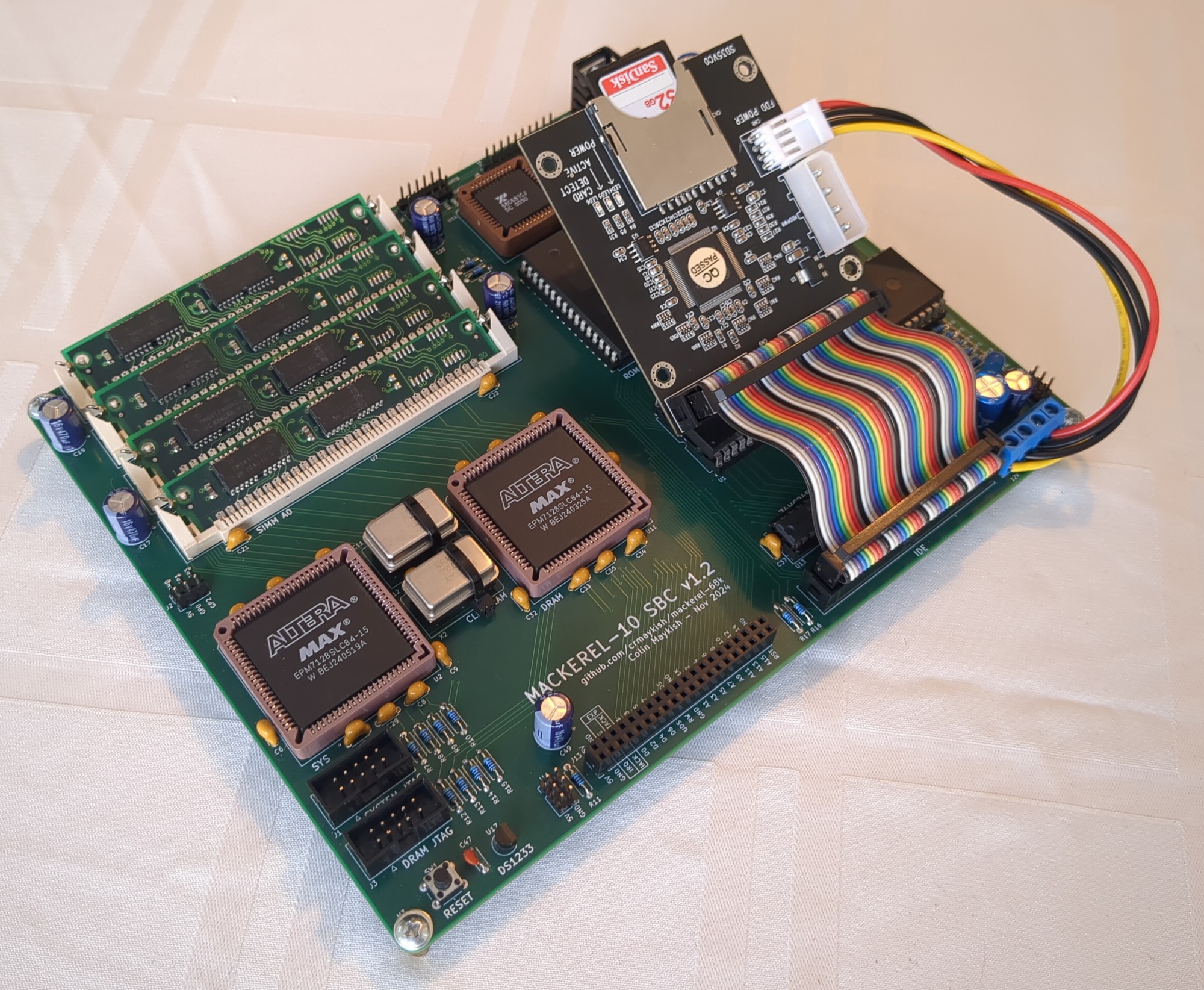
Mackerel-10 v1.2 with IDE drive At this point, I don't have any immediate plans for more hardware changes to Mackerel-10. The current PCB satisfies all of the requirements I had for this system when I started. My focus has shifted to Mackerel-30, but there are still some interesting software options to explore on Mackerel-10.
Mackerel-10 Release Files: https://github.com/crmaykish/mackerel-68k/tree/master/releases/mackerel-10
-
68030 Is Executing Code!
11/25/2024 at 18:17 • 0 commentsThe first prototype of Mackerel-30 is alive! After many hours of soldering, updating Verilog, and modifying memory maps and Makefiles, the 68030 is up and running. Better yet, it's running the same bootloader code as Mackerel-08 and -10 and loading programs over serial. Since the 68030 is more or less a superset of the earlier CPUs, very little C code needs to change from previous iterations of Mackerel.
![]()
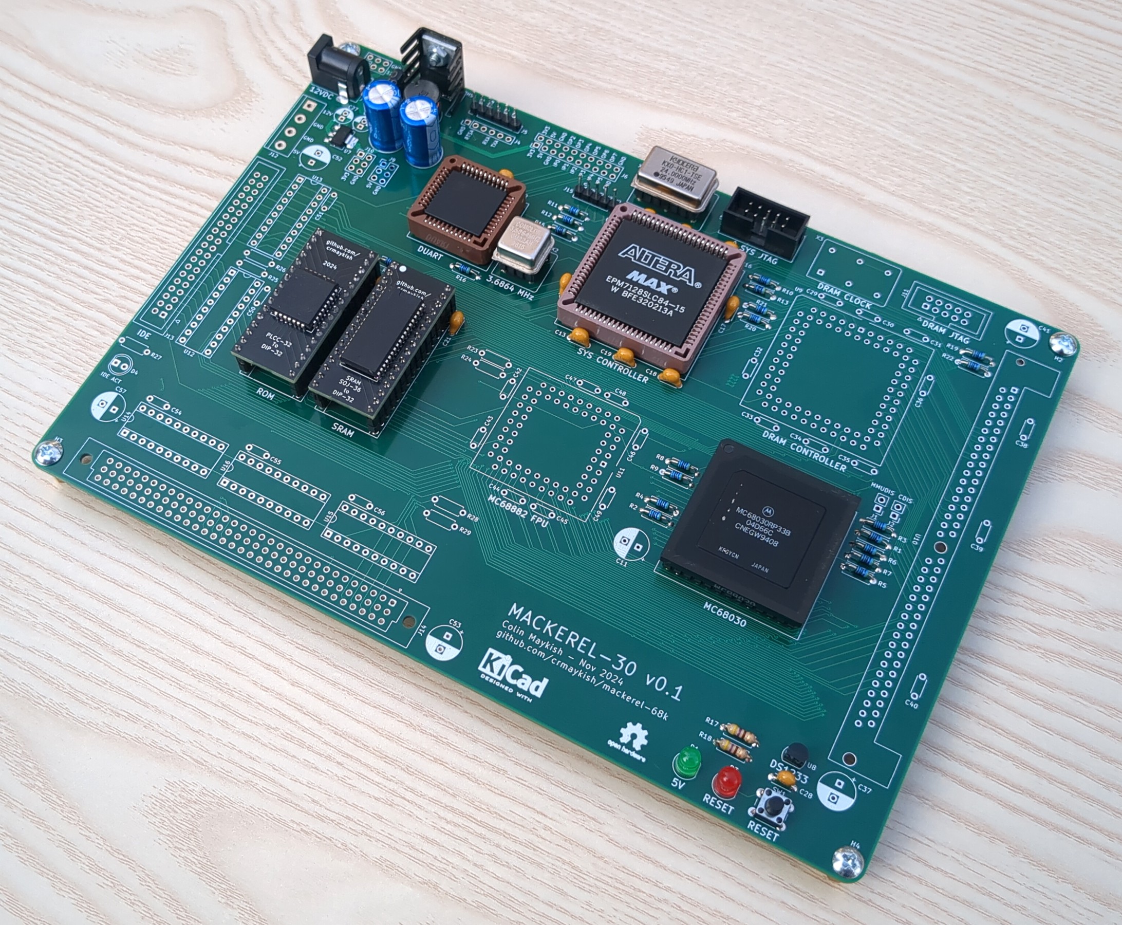
Mackerel-30 v0.1 minimal configuration for board bring-up So far I have verified the basics of the system. Only the ROM, SRAM, and DUART have been tested, but there's enough glue logic implemented to run the bootloader and handle vectored interrupts from the DUART.
Seeing a new design come to life really never gets old. That said, this is a prototype and there are already some problems. For one, the serial header is backwards from previous Mackerel hardware. This caused a slight panic when the code appeared to be running, but no serial output was displayed. Fortunately, flipping the USB-serial adapter solved that issue.
I also managed to export the Gerbers without noticing that the VIN pin of the 3.3v regulator was not connected to anything. I need to figure out why KiCAD didn't complain about this, but the 3.3v power is not actually needed for the board to run, it's just there for external hardware, so no harm done. It's also easy enough to bodge the VIN pin to a nearby 5v rail if necessary.
I haven't hooked up the FPU yet, but I am missing A13-A15 pins on the glue CPLD. I think these are required as part of address decoding for the FPU, so they may need to be bodged in.
Finally, there are a few footprint issues. The mounting holes for the 72-pin SIMM are not all sized correctly, requiring some "plastic surgery" to solder in the socket.
The DIN 41612 connector footprint also has issues. The holes are all way too small to fit the pins of the connectors I have. This is not a custom footprint, it was pulled from the KiCAD library, so it's possible I just have non-standard connectors, but either way, it makes the expansion header pretty unusable.
With the basics working, my plan is to finish assembly and test the DRAM, IDE, and FPU. If at least the DRAM and IDE are functional, I should be able to start on the Linux port. If I find any showstopping issues, I guess Linux will have wait for the next revision.
-
What's New For Mackerel-30?
11/10/2024 at 02:02 • 0 commentsRather than design a bare minimum prototype for Mackerel-30, I decided to take a bit more risk and incorporate most of features I want from the start. Moving from the 68008 to the 68010 was a reasonable step up in complexity. Jumping to the 68030 presents another significant leap with 32-bit buses and more complicated control logic. In some ways, it's actually easier to deal with though. The dynamic bus sizing removes the requirement for 16-bit ROM and RAM chips. A single 8-bit ROM and SRAM should be enough to bootstrap the system.
Besides the new CPU, I've included a few other hardware upgrades. I'm looking forward to getting the MC68882 FPU up and running. It should be supported by Linux and might give a boost in performance for things like scripting languages or graphics support if and when I get to those.
I've also upgraded to 72-pin SIMMs for the DRAM. Each SIMM is 32-bits wide which makes the wiring straightforward and requires only a single module. The available capacities are also quite a bit higher than 30-pin modules, going up to at least 128MB. The DRAM controller will be adapted from the one I designed for Mackerel-10.
The only piece I have not included in this first prototype is networking hardware. I'm still exploring some options in this area and I'm not ready to commit to one design. Once the base system is brought up, I plan to build a network card to connect to the expansion header.
![]()
-
Another Word On DRAM
10/25/2024 at 04:15 • 0 commentsGetting a DRAM controller working at all feels like a great accomplishment, and while it has been stable and functional, there were some situations I couldn't explain. For example, it was not possible to run the DRAM controller at anything other than twice the CPU speed, even running them at the same frequency failed completely. I was not satisfied with my understanding of my own design. I also wanted the option to run the DRAM on its own independent clock to completely free up the choice of oscillator for the CPU.
With the goal of better understanding and more flexibility, I took the lessons learned from my first iteration and went back to the drawing board, starting with the datasheet. The simplest place to start is the CAS-before-RAS refresh.
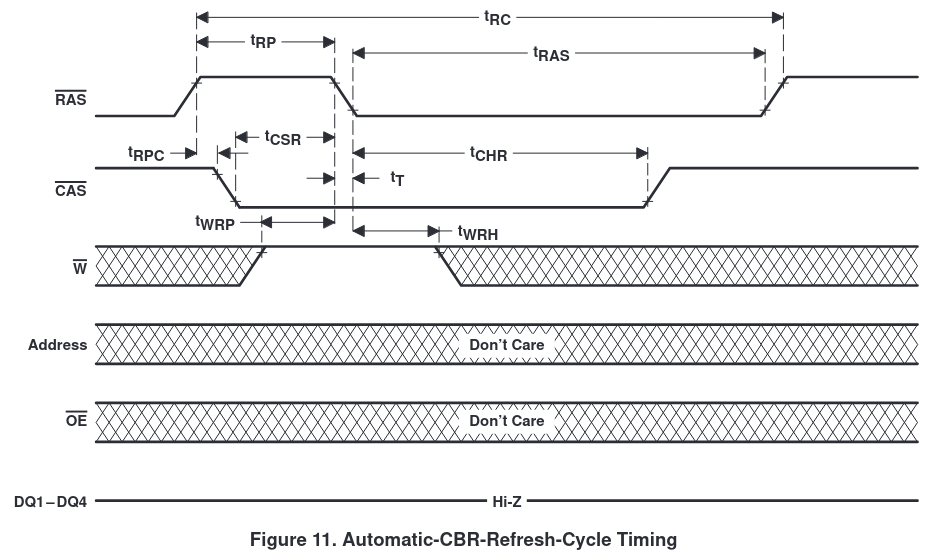
CAS-before-RAS Refresh
![]()
CAS-before-RAS refresh timing diagram from the TMS417400 datasheet The refresh process is not complicated: pull CAS low, then pull RAS low, raise CAS, and then raise RAS again. One thing worth noting here is that the WE pin has to be HIGH by the time RAS is lowered. Since the state of the WE pin is "don't care" for the rest of the refresh cycle, I chose to pull it HIGH in the first state of the refresh state machine. Note: Mackerel-10 has four 30-pin SIMMs in two 16-bit pairs, A and B. RAS is shared between SIMMs in a pair, but the CAS lines are all independent, thus two RAS pins and four CAS pins in my controller.
REFRESH1: begin
    // Acknowledge the refresh request
    refresh_ack <= 1'b1;

    // Lower CAS
    CASA0 <= 1'b0;
    CASA1 <= 1'b0;
    CASB0 <= 1'b0;
    CASB1 <= 1'b0;
    WRA <= 1'b1;
    WRB <= 1'b1;
    state <= REFRESH2;
end

REFRESH2: begin
    // Lower RAS
    RASA <= 1'b0;
    RASB <= 1'b0;
    state <= REFRESH3;
end

REFRESH3: begin
    // Raise CAS
    CASA0 <= 1'b1;
    CASA1 <= 1'b1;
    CASB0 <= 1'b1;
    CASB1 <= 1'b1;
    state <= REFRESH4;
end

REFRESH4: begin
    // Raise RAS
    RASA <= 1'b1;
    RASB <= 1'b1;
    state <= PRECHARGE;
end
The final piece of the DRAM refresh cycle is determining how often it needs to happen. According to the datasheet, all 2048 rows need to be refreshed every 32 ms. If we refresh each cell incrementally with CBR, that means we need to refresh a cell every 32 ms / 2048 = 0.015625 ms. That equates to 64 kHz. Finally, the DRAM controller is running from a 50 MHz oscillator, so 50 MHz / 64 kHz = 781 cycles between refreshes.
The Verilog for counting cycles is basic, but I'll include it here for reference. The two refresh_ registers are used to pass the refresh state back and forth between this generator code and the main state machine. REFRESH_CYCLE_CNT is set to 781.
// ==== Periodic refresh generator reg refresh_request = 1'b0; reg refresh_ack = 1'b0; reg [11:0] cycle_count = 12'b0; always @(posedge CLK_ALT) begin if (~RST) cycle_count <= 12'b0; else begin cycle_count <= cycle_count + 12'b1; if (cycle_count == REFRESH_CYCLE_CNT) begin refresh_request <= 1'b1; cycle_count <= 12'b0; end if (refresh_ack) refresh_request <= 1'b0; end end![]()
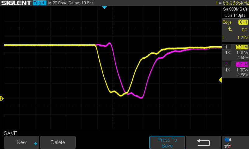
CAS-before-RAS refresh cycle running at 64 kHz as calculated Read/Write Cycles
With the CBR refresh behavior confirmed, I started to revamp the rest of the state machine, i.e. the process of actually reading and writing memory. As mentioned, my first implementation worked, but just barely. One of the issues I had was a dozen or more compiler warnings in Quartus that looked something like this: Warning (163076): Macrocell buffer inserted after node. I could not track down an exact cause, but the little information I found online and my own testing seemed to indicate that this error basically means "you're trying to do much work at once". By breaking up my state machine into more smaller states and removing highly parallel pieces of code, I was able to get rid of all all these warnings. It seems like the key is not to change too many register values per clock cycle, but to instead pipeline the design.
![]()
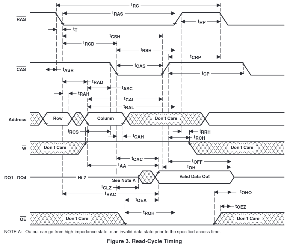
DRAM read cycle timing diagram from the TMS417400 datasheet The actual logic of the DRAM read and write cycles hasn't changed. It's still a multi-step process where the controller multiplexes the CPU address bus to the row address of the DRAM, asserts /RAS, multiplexes the column address, then asserts /CAS and /DTACK until the CPU finishes the bus cycle. Here's a snippet of the state machine showing this piece:
IDLE: begin
    if (refresh_request) begin
        // Start CAS-before-RAS refresh cycle
        state <= REFRESH1;
    end
    else if (~CS2 && ~AS2) begin
        // DRAM selected, start normal R/W cycle
        state <= RW1;
    end
end

RW1: begin
    // Mux in the address
    ADDR_OUT <= ADDR_IN[11:1];
    state <= RW2;
end

RW2: begin
    // Row address is valid, lower RAS
    if (BANK_A) RASA <= 1'b0;
    else RASB <= 1'b0;
    state <= RW3;
end

RW3: begin
    // Mux in the column address
    ADDR_OUT <= ADDR_IN[22:12];

    // Set the WE line
    if (BANK_A) WRA <= RW;
    else WRB <= RW;

    state <= RW4;
end

RW4: begin
    // Column address is valid, lower CAS
    if (BANK_A) begin
        CASA0 <= LDS;
        CASA1 <= UDS;
    end
    else begin
        CASB0 <= LDS;
        CASB1 <= UDS;
    end
    state <= RW5;
end

RW5: begin
    // Data is valid, lower DTACK
    DTACK_DRAM <= 1'b0;

    // When AS returns high, the bus cycle is complete
    if (AS) state <= PRECHARGE;
end
And here's what it looks like in simulation:
![]()
Simulation of the DRAM controller reading memory There are more stages than in my previous version, but each stage is doing a small and obvious thing. It's tempting to try to combine some of these steps together, and there's probably room for optimization, but clarity and stability are the priorities at the moment.
Crossing Clock Domains
The final piece I wanted to tackle was having the ability to run the DRAM controller at any speed, not having it tied to a multiple of the CPU frequency. Because DRAM takes more cycles to access than SRAM, the whole system is slower clock-for-clock. It's not a dramatic difference, but those extra clock cycles add up. One way to alleviate some of this delay is to run the DRAM controller at a faster clock than the CPU. This shouldn't be too hard. Most 68000s are only rated to 10 MHz or so. The CPLD running the DRAM controller can easily handle 50 MHz. With this arrangement, most or all of the extra cycles taken up by DRAM access happen between the slower CPU cycles.
In a perfect world, this change would be as simple as connecting a second faster oscillator to the DRAM controller and updating the CLK pin. In reality, this leads to metastability. I won't try to explain that concept here as I'm just coming to terms with it myself, but the outcome is that there needs to be a bit of a handoff when referencing the slow CPU signals from the fast DRAM clock cycles. This is called crossing clock domains and it's accomplished by double registering the slower signals before using them in the faster domain. Fortunately, Mackerel only has two input signals that fit that description: CS and AS.
reg AS1 = 1;
reg CS1 = 1;
reg AS2 = 1;
reg CS2 = 1;

always @(posedge CLK_ALT) begin
    AS1 <= AS;
    CS1 <= CS;
    AS2 <= AS1;
    CS2 <= CS1;
end
Double-flopping the DRAM chip-select pin and the CPU's /AS pin like this virtually guarantees that the DRAM controller won't sample them during a transition (the cause of metastability). CS2 and AS2 are now nice and stable in the DRAM's clock domain and they can be used to kick off the DRAM access process (see the IDLE state in the Verilog above).
We've now removed the link between the CPU clock and the DRAM controller. This does not scale infinitely. There are some limitations on the differences between the clocks, but it's dramatically more flexible than my last attempt. In testing, I was able to run the DRAM controller at 50 MHz with the CPU clock anywhere between 9 and 20 MHz. It's also possible to remove the double-flopping and run on one synchronized clock, something I could not do previously.
Wrapping Up
Implementing a DRAM controller for a 40 year old CPU on a 20 year old CPLD is quite a niche subject, but this is the information I wish I had when I started working on this. Hopefully this is helpful to somebody. If that's you, share your project. I'd love to hear what you're working on!
Here is the full Verilog code for the DRAM controller: https://github.com/crmaykish/mackerel-68k/blob/master/pld/mackerel-10/dram_controller/dram_controller.v
-
Linux IDE Driver And Hardware Updates
10/20/2024 at 22:27 • 2 commentsI've been making steady progress on Mackerel-10 since initial board bringup. The most exciting development is a working Linux driver for the IDE interface. There's now a real /dev/hda device accessible and this comes with all of the built in tools and filesystem support from the kernel. After adding fdisk and mkfs to the Linux image, the IDE drive can be partitioned and mounted as a persistent storage device right from Linux. This is a huge step in improving the usability of the system and it's a milestone for the project as a whole.
![]()
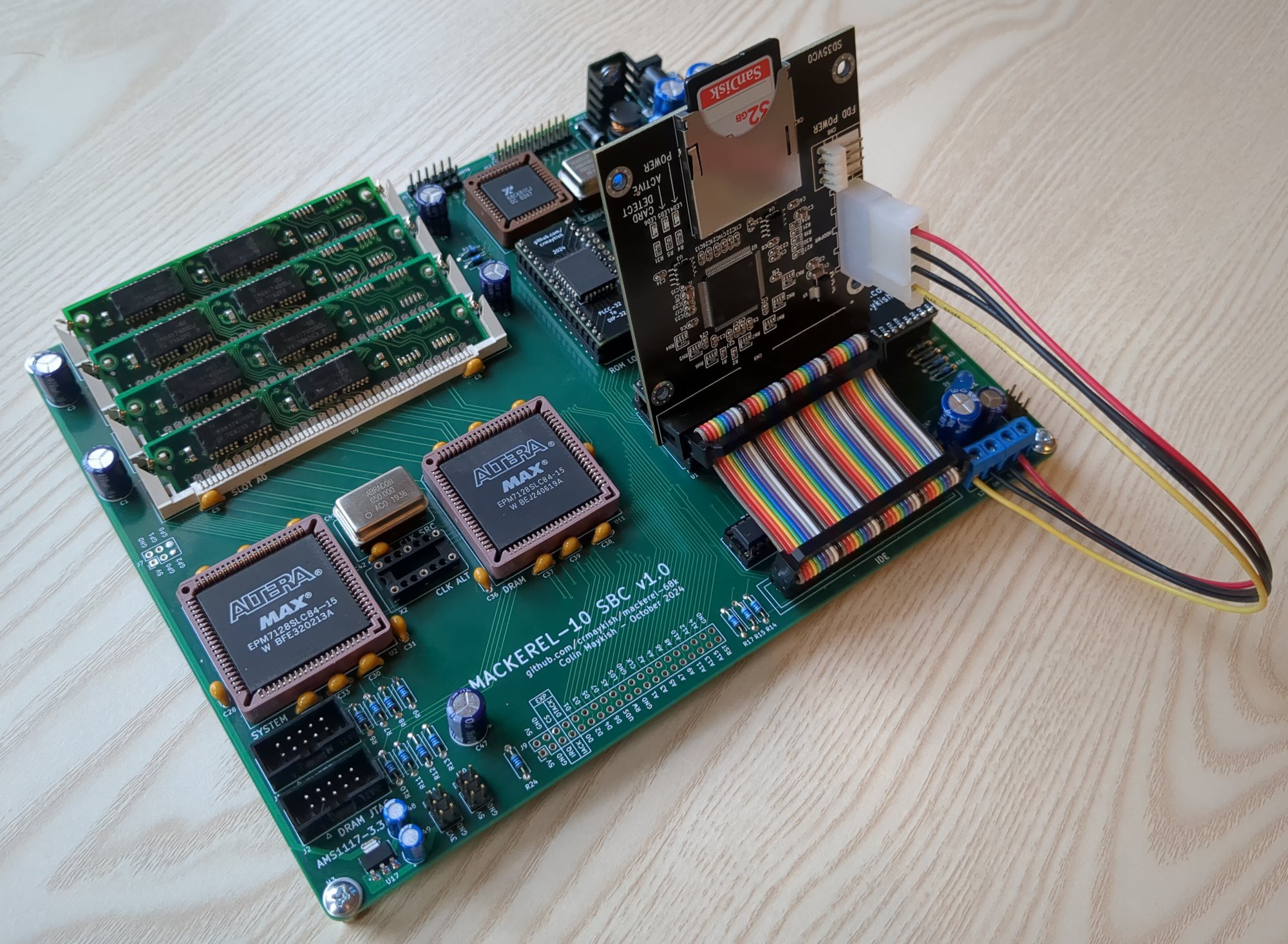
Mackerel-10 with SD-to-IDE adapter Hardware Changes and Glue Logic
The hardware design of the IDE interface was mostly complete before I started work on the driver, but there were a few updates to get everything fully supported. While it's possible to use IDE devices without interrupts, the Linux driver interface requires a working interrupt from the drive. This interrupt pin was already routed to the CPLD, so I updated the interrupt control Verilog to handle the extra source.
The only sticking point on the wiring side was the missing second chip select line. IDE devices have two CS pins: CS0 and CS1. Only CS0 is required for basic functionality, but CS1 enables access to the alternate status register, a.k.a. the device control register. This register is needed to control interrupts on the drive. I did not have this pin connected to the CPLD, but it was connected to 5v through a pull-up, so I bodged a connection to one of the spare IO pins on the CPLD and updated the address decoding to make this device control register accessible to the CPU.
Writing a Linux IDE Driver
With the hardware and glue logic updated and tested in isolation, I started work on a Linux driver. There are a few different ways to implement IDE on Linux. The traditional (i.e. deprecated) way is to implement an ide_host and the associated functions for communicated with the drive(s). There's also a newer approach based on libata. This is a more modern solution, but it is not supported on m68k architecture, at least in the 4.4 kernel I'm running, so I implemented the traditional driver.
Conceptually, the IDE driver interface is pretty simple. There are a handful of operations that the driver needs to define and the driver requires an interrupt number. On Mackerel-10, the IDE interrupt is autovectored to IRQ number 3. Implementing the required functions is fairly straightforward. For example, here are the commands that read the status, execute IDE commands, and read blocks of data:
static u8 mackerel_ide_read_status(ide_hwif_t *hwif)
{
    return MEM(MACKEREL_IDE_STATUS);
}

static void mackerel_ide_exec_command(ide_hwif_t *hwif, u8 cmd)
{
    MEM(MACKEREL_IDE_COMMAND) = cmd;
}

static void mackerel_ide_input_data(ide_drive_t *drive, struct ide_cmd *cmd, void *buf, unsigned int len)
{
    int i;
    int count = (len + 1) / 2;
    u16 *ptr = (u16 *)buf;

    for (i = 0; i < count; i++)
    {
        ptr[i] = MEM16(MACKEREL_IDE_DATA);
    }
}
The full driver code is available here: https://github.com/crmaykish/mackerel-uclinux-20160919/blob/master/linux/drivers/ide/mackerel-ide.c
Dirty Hacks
One issue remains with this driver. Normally, when an IDE interrupt is generated, the drive will assert the IRQ line and hold it until the CPU reads the status register. This clears the interrupt and normal operation resumes. For some reason, the interrupt on my system is never getting cleared. This means that after the first IDE interrupt, the driver just hangs and the system can't boot further.
I managed to "solve" this by reading the status register manually in the process_int() function in ints.c if the vector number matches the IDE IRQ number, but this is a total hack. I don't know why the driver is not doing this automatically. It's entirely possible there's an issue with my interrupt glue logic or something dumb I missed in the driver code itself. I need to figure this out, but my hack is working for now and the IDE driver is fully functional.
![]()
IDE drive partitioned with a 100MB ext2 filesystem Other Hardware Updates
Lastly, I've made a few smaller changes to the hardware configuration. I removed the two SRAM chips and mapped the DRAM from 0x000000 to 0xF00000, so all 15MB of RAM are now served by DRAM. I'd like to do some benchmarking and see if repurposing the SRAM for the stack area would improve performance at all since it requires fewer CPU cycles to access compared to DRAM, but I haven't noticed any obvious changes in usability when running uClinux with only DRAM.
I've also been experimenting with the CPU clock speed as this translates directly to system performance. Using the 68010 rated for 10 MHz, I was able to run with a slight overclock to 12 MHz with the DRAM controller running at 24 MHz, but anything higher was causing instability. When I installed the M68SEC000 rated for 20 MHz, I was able to push all the way to 25MHz for the CPU clock and 50 MHz for the DRAM. This shows that the DRAM controller is not the bottleneck, but the 68010 I have just doesn't have much headroom. That's fine. There are other options like the 68HC000 which push the speeds higher, or I can just continue using the SEC on my adapter board. I still need to experiment with running the DRAM controller and CPU on independent clocks.
![]()
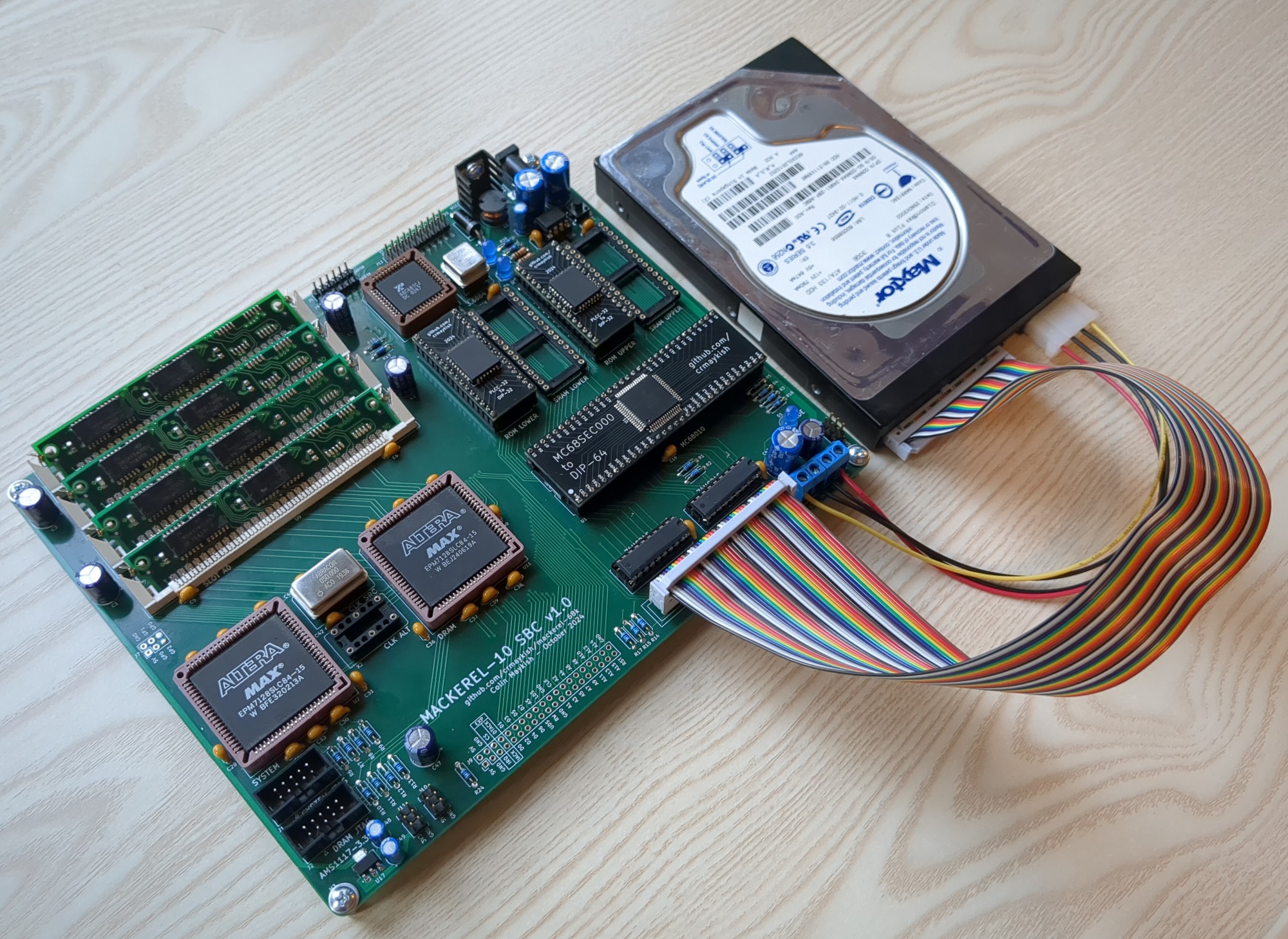
Current state of the hardware - SEC CPU at 25 MHz, 16MB of DRAM, 3.5" IDE hard drive Getting Close
Mackerel-10 is really coming together as a fun little computer and a significant upgrade to Mackerel-08. Based on my original plan of adding DRAM and IDE support, it's complete. There are a few more software updates I'd like to make, including booting Linux from the IDE drive instead of relying on a ROMFS. I'm also planning another PCB revision to resolve some of the design issues and incorporate the bodges into the circuit properly.
I've started rough planning for the next iteration in the project, Mackerel-30, but I am having a lot of fun playing with Mackerel-10 and I'm not in a rush to mark it complete and move on just yet.
-
Mackerel-10 v1: Lots of DRAM And A Hard Drive
10/17/2024 at 16:54 • 0 commentsThe first round of PCBs for the Mackerel-10 SBC are in and I've begun assembly and board bringup. There aren't too many software changes going from the prototype to v1, but the hardware changed a little bit. There are now four 30-pin SIMM slots instead of two. These are arranged in two pairs to allow a 4x4MB DRAM configuration. Additionally, the IDE interface is now buffered through a set of 74HC245 chips to handle longer ribbon cables. The upper and lower bytes of the 16-bit IDE interface are also swapped in the layout to transparently convert the IDE little-endianness to the 68k's big-endianness. Finally, the pinouts of both CPLDs were completely changed to facilitate the routing of this board, so all of the pin mappings had to be updated in the Verilog projects.
![]()
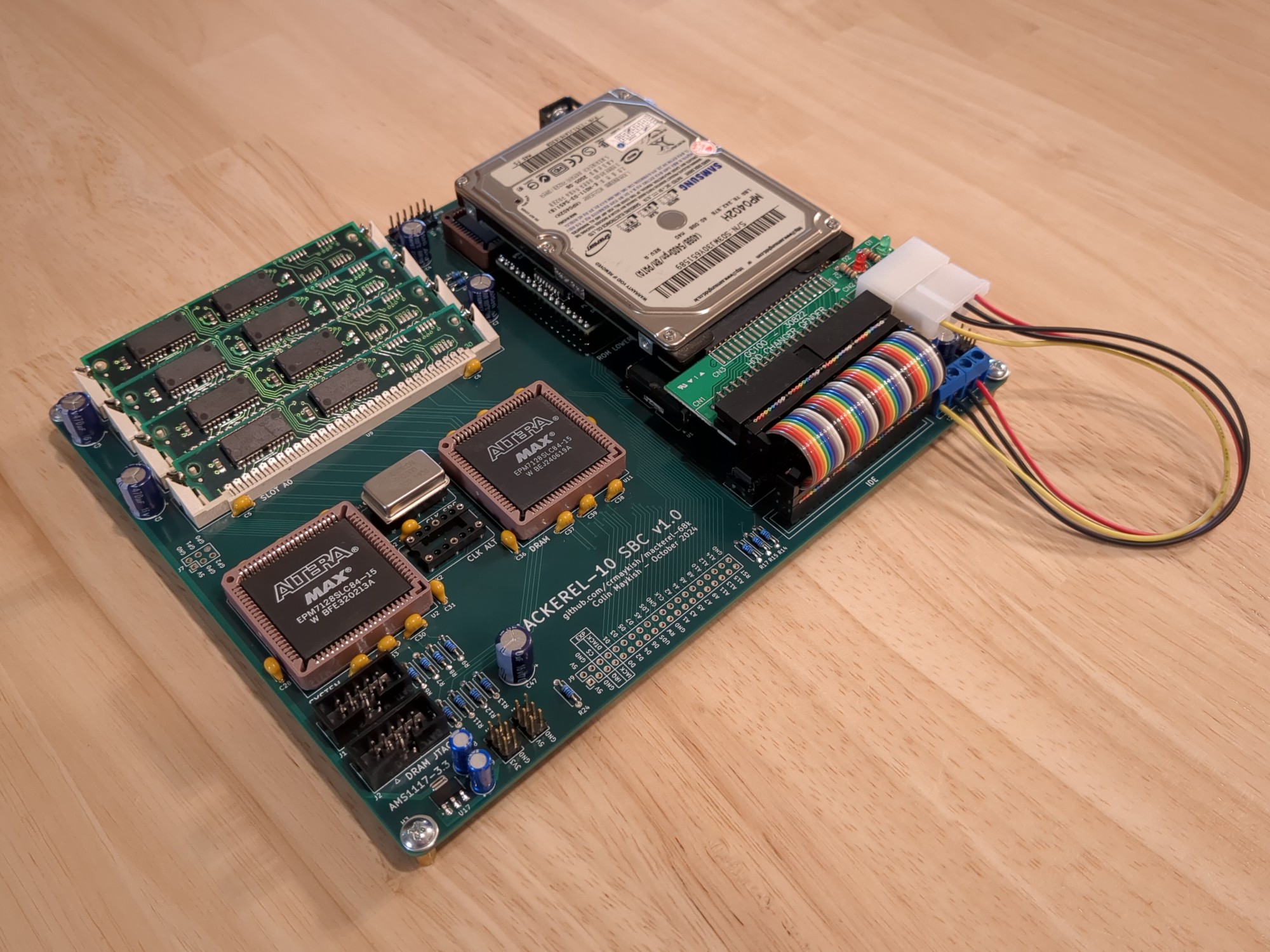
Mackerel-10 SBC v1 assembled The core system (CPU, ROM, SRAM, DUART) came up pretty quickly once the glue logic and memory map was updated. The DRAM controller also works as expected. I had to update the DRAM controller to handle the extra two SIMM slots, but Mackerel-10 now has access to 14MB of DRAM. One megabyte is still used by the SRAM and the ROM and I/O share the remaining megabyte of address space. All in, that means we've now got 15MB of usable RAM on board.
My DRAM controller is currently running fairly slowly (12.5MHz) at twice the CPU clock frequency (6.25 MHz). I added a second oscillator to the CPLDs with the hope of running the CPU and the DRAM controller on independent clocks, but I have not spent any time working on this. Ideally, the DRAM controller runs at whatever maximum frequency it can without having to worry about being in sync with the CPU clock. Since the DRAM bus access is asynchronous using its own DTACK signal, this should be possible, but I'll need to do some experimentaton and timing analysis.
The new IDE interface caused me some trouble. In the prototype, the 16-bit data bus from the CPU was wired directly to the IDE drive. Adding buffers between them will help with stability and lighten the load on the CPU data bus, but it adds a little more complexity and enough room to screw something up, which I did. After a lot of debugging with the oscilloscope, I realized the buffers are working fine, but the direction pin was inverted (or the A and B buses on the buffers were inverted, depending on your perspective). This meant the buffers were always pointing the wrong direction when the CPU tried to access the IDE registers. This was a dumb mistake I made in the schematic, but I was able to fix it by cutting the trace from the RW pin to the DIR pins on the buffers and creating the proper direction signal from one of the spare CPLD pins. With this bodge in place, IDE was functioning again.
![]()
Bodge to fix the direction pin of the IDE buffers There is minimal software support for IDE devices at the moment, but Mackerel-10 can read and write arbitrary sectors from the disk and print out drive identification info. I've done most of my testing with a SD-to-IDE adapter for simplicity, but I wanted to hook up a real IDE hard drive to make sure that was also working.
![]()
Mackerel-10 with a real 2.5 inch IDE hard drive I'm a little disappointed about the IDE bodge, but I'm really pleased with the overall SBC. There are a few other minor issues with the v1 design that I will address in a future PCB revision, but my focus will now turn back to the uClinux port. I have a lot more RAM to play with and a real IDE device opens up a lot of options, at least once I figure out how to write a driver for it.
-
Mackerel-10 v1 PCB Design
10/05/2024 at 23:09 • 0 commentsIn my last couple posts, I described the DRAM controller and IDE interface I've been working on. With both features working reliably, it's time to combine them together and build an SBC. One element I did not consider when making the jump from the 68008 to the 68010 is how much more complicated the actual PCB routing would be with all those extra pins. The DRAM controller also adds a lot of complexity to the routing and takes up a lot of board space.
I designed Mackerel-10 v1 as a four-layer board with the same stack-up as Mackerel-08, signal/ground/power/signal. The circuit design is not drastically different than the prototype PCBs I've been working with until now. The main difference is the on board IDE header and the addition of two extra SIMM slots. I wanted the option to use 4x4MB DRAM.
I also broke out more I/O from the DUART and more power pins in general. I decided to keep the system expansion header limited to an 8-bit data bus with A1-A15 exposed, plus enough control signals to attach reasonable I/O devices. It did not feel necessary to expose the full 16-bit data bus or all of the address pins when most of the address space will be filled with on-board DRAM anyway.
Finally, I added an optional second clock oscillator to both the system and DRAM CPLDs. I'd like to experiment with running the DRAM state machine on its own clock in an attempt to maximize both the CPU speed and the DRAM access efficiency.
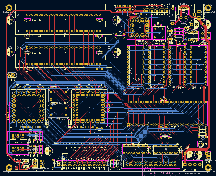
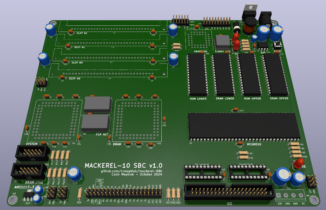
This is the biggest and most complex board I've routed so far. PCB manufacturing prices don't increase that substantially as the board size grows, so I did not go crazy trying to keep it as small as possible. It ended up being 210x170mm.
![]()
Mackerel-10 v1 PCB signal layers ![]()
Mackerel-10 v1 PCB render -
Connecting an IDE Drive
09/23/2024 at 02:57 • 0 commentsWith DRAM implemented, the next step for Mackerel-10 is to add support for IDE storage. Mackerel-08 has rudimentary persistent storage in the form of an SD card connected to the XR68C681's GPIO. The bitbang SPI protocol technically works, but it is incredibly slow. It takes about 4 minutes to load the 1.5MB kernel into RAM from the SD card. For Mackerel-10, I want something faster and more robust.
IDE is actually somewhat of a natural choice for the 68000. Although the protocol has its roots in the x86 world, it's a fairly simple 16-bit memory-mapped register interface. It's possible to connect the full 16 data lines, 3 address lines, and a handful of control signals from an IDE drive directly to the 68000 with only a small amount of glue logic. I did just that.
![]()
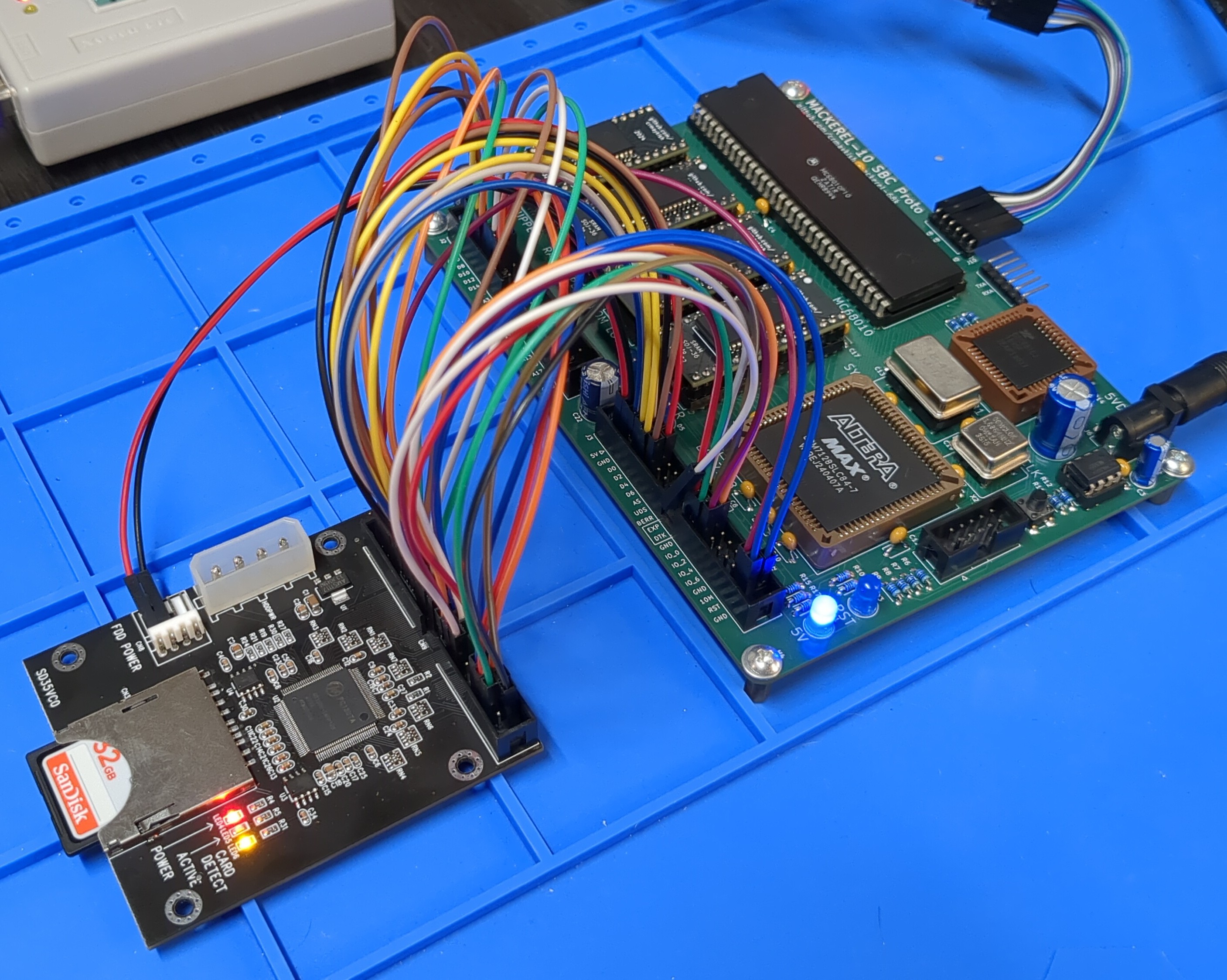
Mackerel-10 prototype wired to an SD-to-IDE board Ignoring interrupts and DMA for now, the only signals that don't map directly between the 68000 and the IDE interface are the chip selects and the read/write lines. IDE splits read and write into two pins instead of the single /RW pin of the 68000. I updated the glue logic in the CPLD to create the required signals and I put together some really basic C code to talk to the IDE device.
The IDE protocol is actually really in depth, but for basic functionality, there's only a few pieces that matter. There are registers for data, status, error, and setting sector values and there's a command register with a list of supported commands. I've implemented two of these commands: DEVICE_IDENTIFY (0xEC) and READ_SECTOR (0x20).
This is enough to read device info, e.g. model, firmware, and capacity details and to read arbitrary sectors of data from the drive. Sectors are transferred as 256x16 bit words. The only sticking point is that IDE, like x86, is little-endian and 68000 is big-endian so each word has to have the high and low bytes swapped. I've chosen to do this in code for now, but I've seen other projects implement this in hardware by simply wiring the data bus connection between the CPU and the IDE drive with the swap built in.
It would have been nice to combine this IDE prototype and the DRAM breakout board to get a sense of what the full Mackerel-10 SBC will look like, but I did not think to design that option into the prototype PCBs. Oh well. I'm feeling good about this IDE test and my DRAM board has been very stable as well. I think it's time to jump back into KiCAD and start building the Mackerel-10 v1 PCB.
Mackerel-68k Linux SBCs
A series of m68k-based single-board computers built to run Linux
 Colin M