-
Build Progress
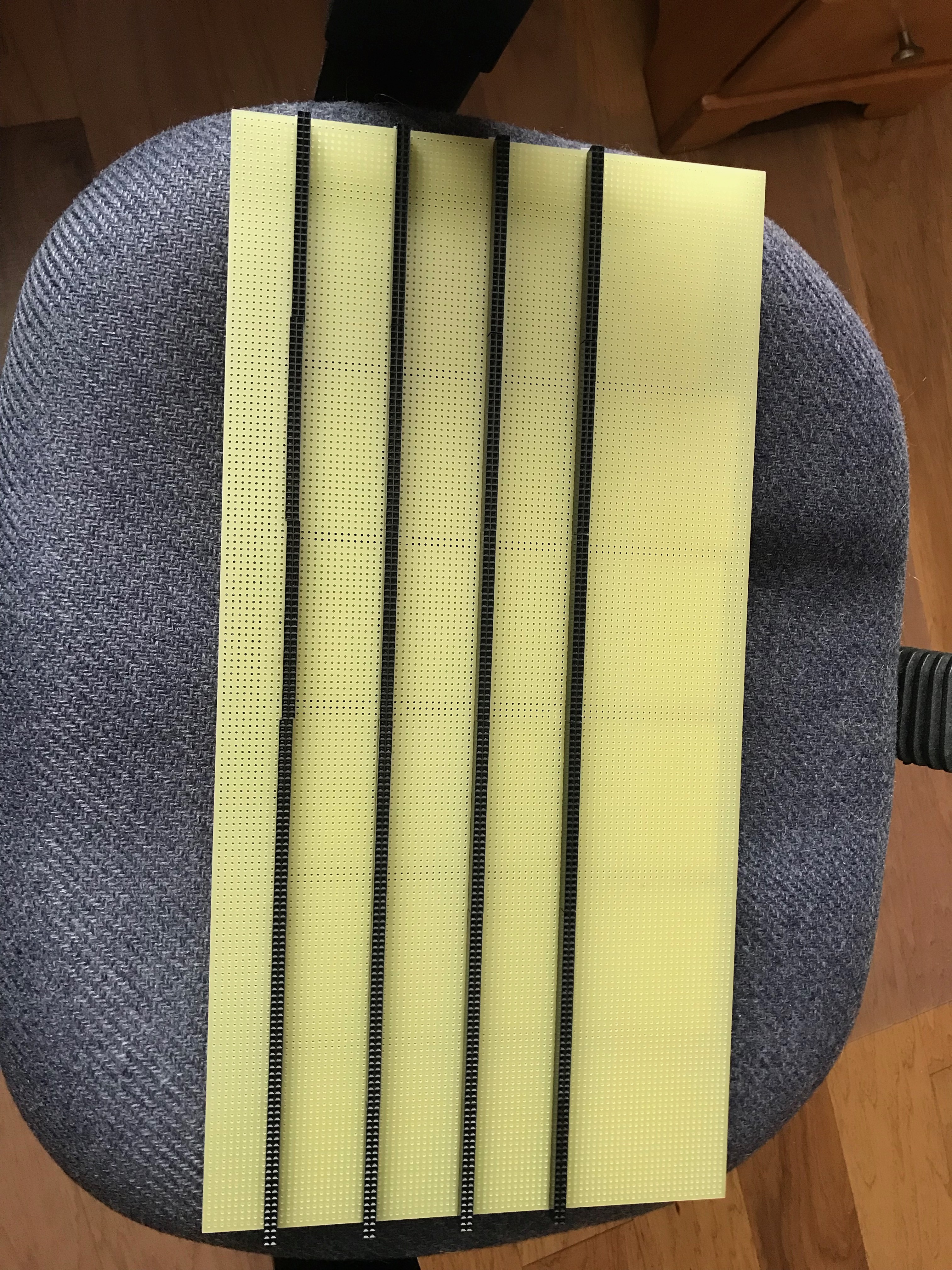
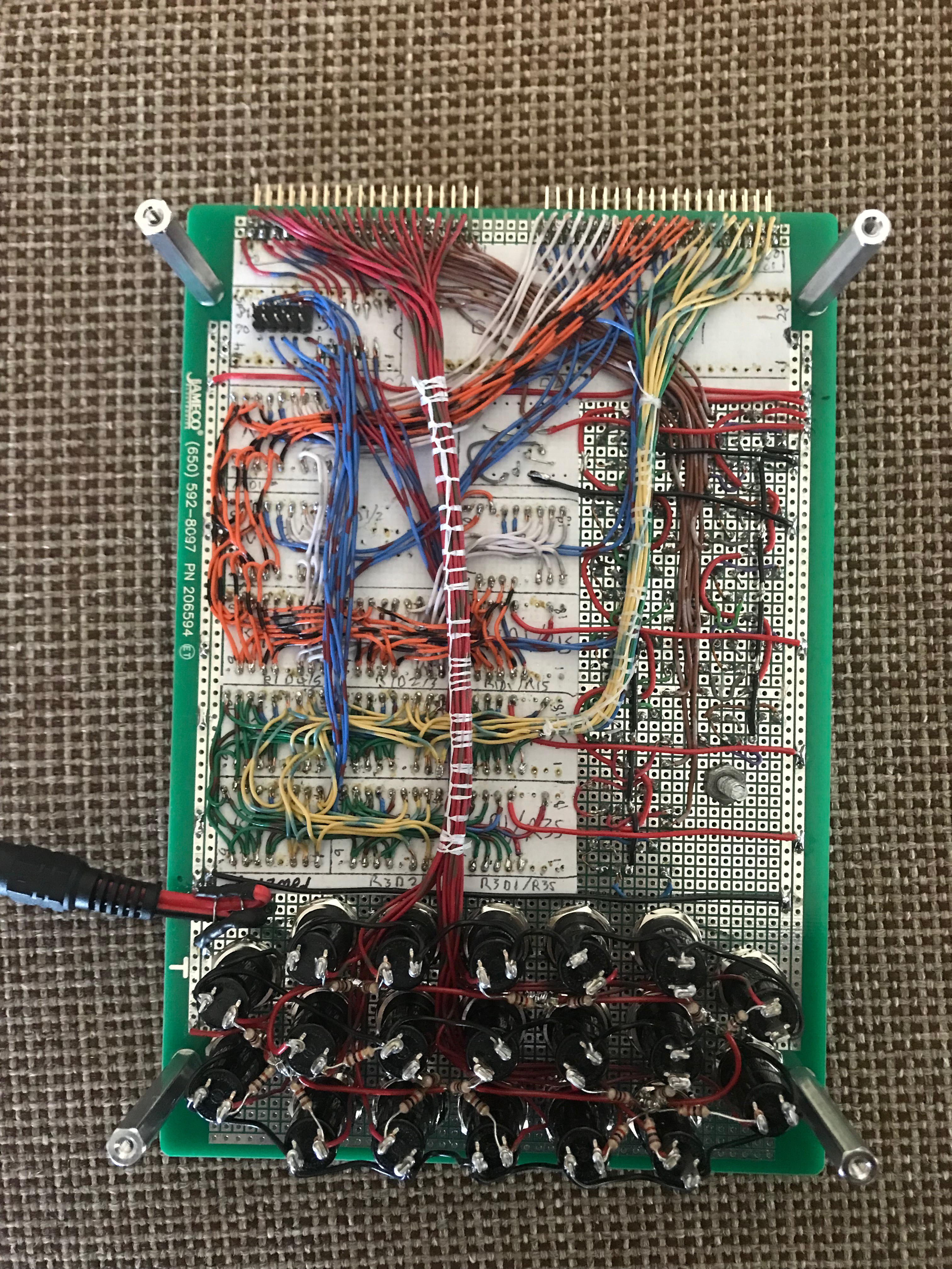
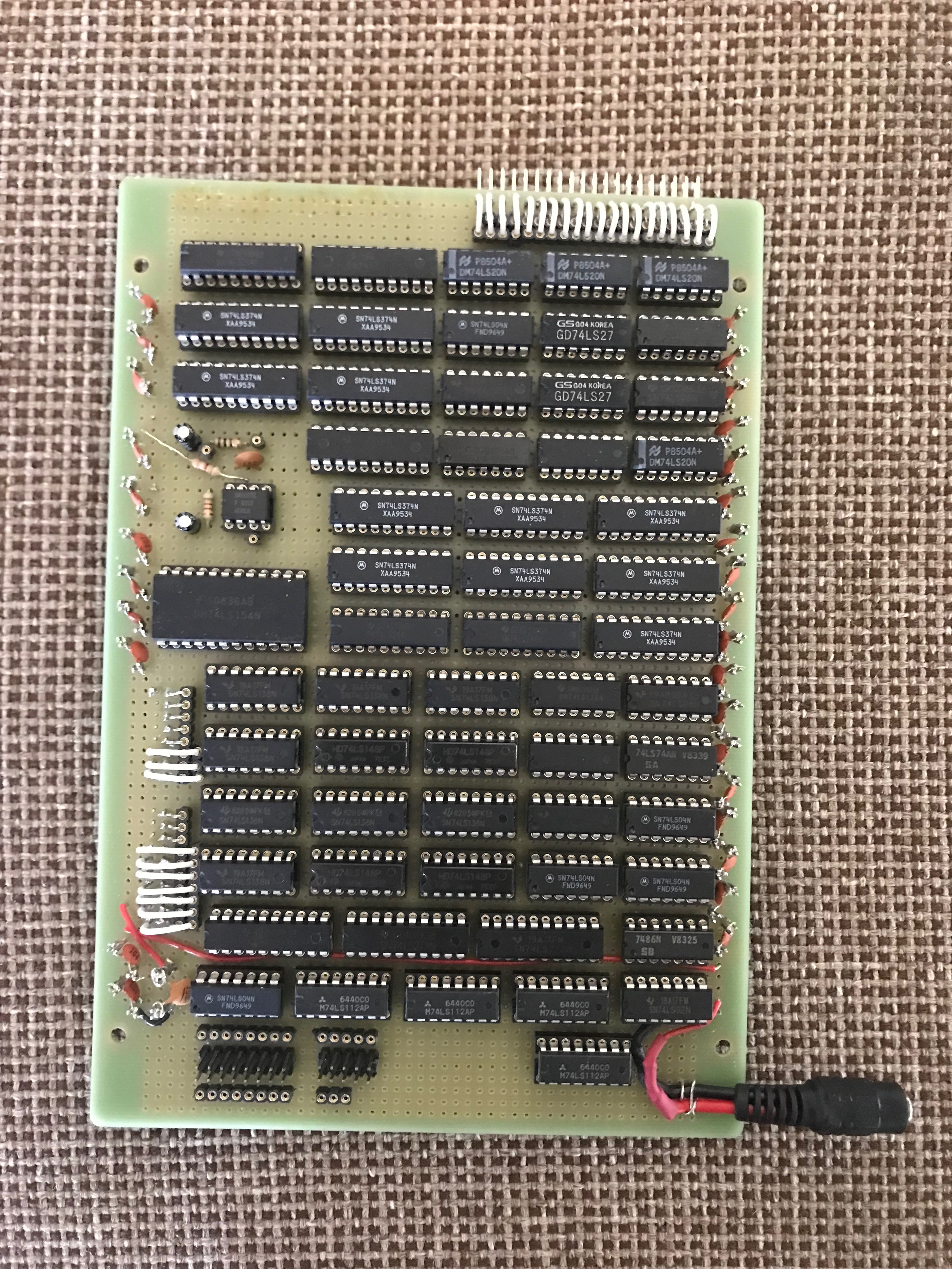
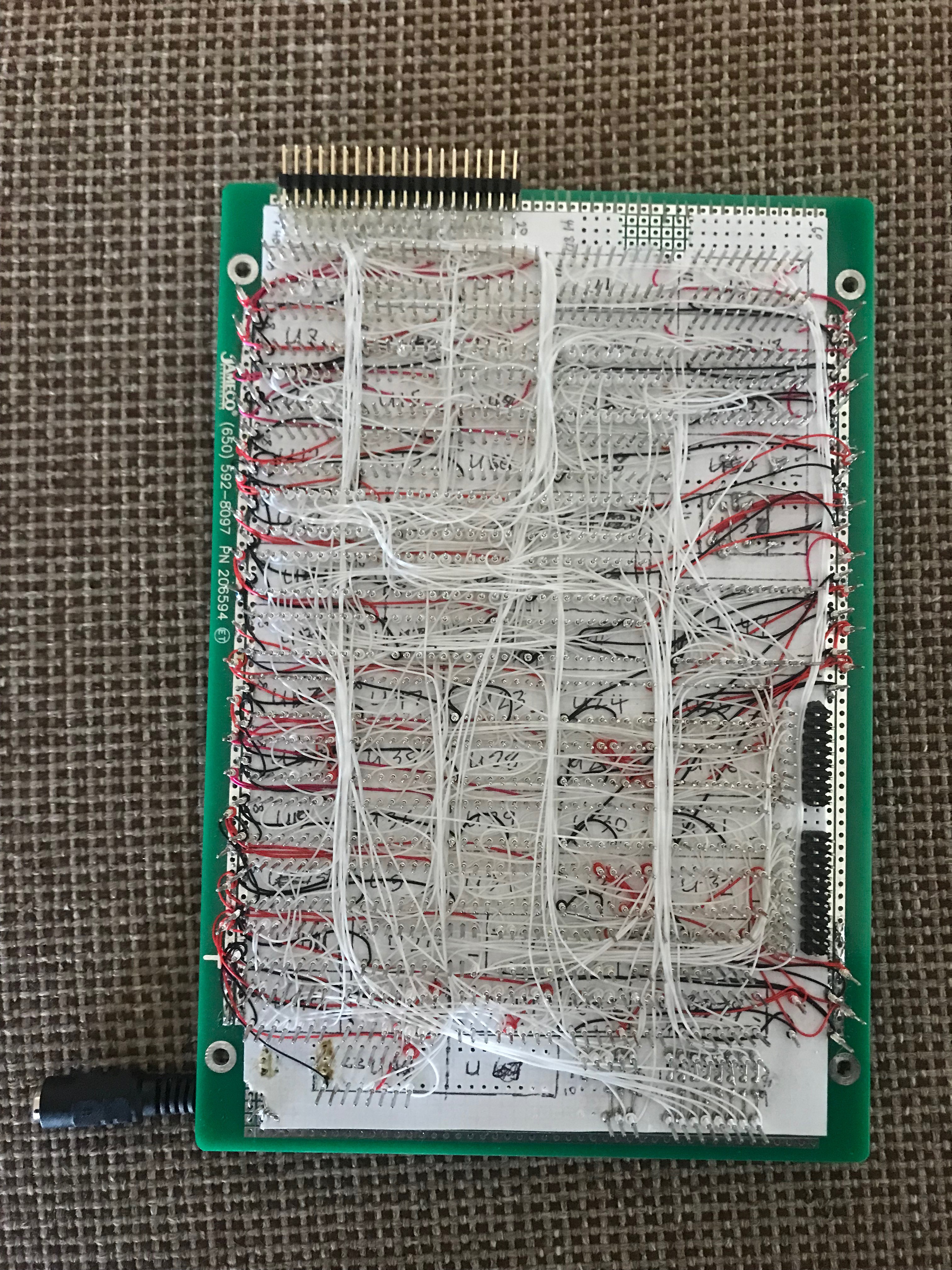
11/08/2024 at 16:43 • 0 commentsAfter three years I have started back up on this project. When I left off the display board and backplane were complete and the memory board was partially complete. The idea was that the board under test would be moved to the last slot of the board stack. The realization that all three boards would have to be debugged simultaneously led me to the conclusion that the board configuration would have to be modified. This has been the first issue to attack before getting back to then fun of wiring chips together. The new plan is to have all four boards exist in one plane that will eventually be placed into a frame, probably hinged down the middle. The boards will still need to be connected with various ribbon cables. The data cables defined before will remain the same, only their location on the boards will change. The display cables will change quite a bit since there will no longer be a backplane. A portion of the existing backplane was cut off. This will become a breakout board that plugs onto the bottom of the existing display board. Each group of pins relates to displaying things like registers and control pulses. These pins have been grouped into either 8, 16 or 20 bits. Each of these connectors route to only one other board. The other three boards will have these display connectors on the bottom edge instead of the huge backplane connector as before. This simplifies things significantly. The display board will have the LEDs face out and the other three boards will have the wire wrap side face out.
This is the configuration that makes the most sense.
![]()
![]()
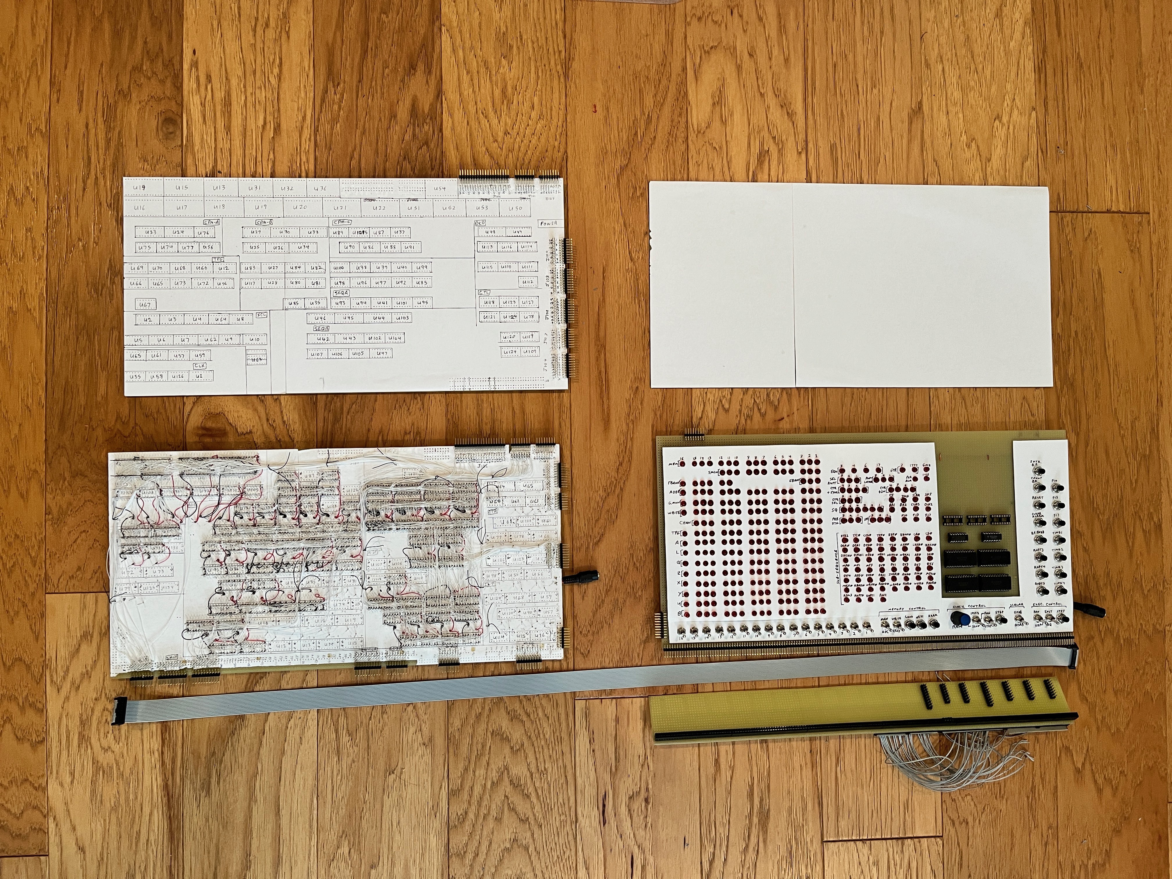
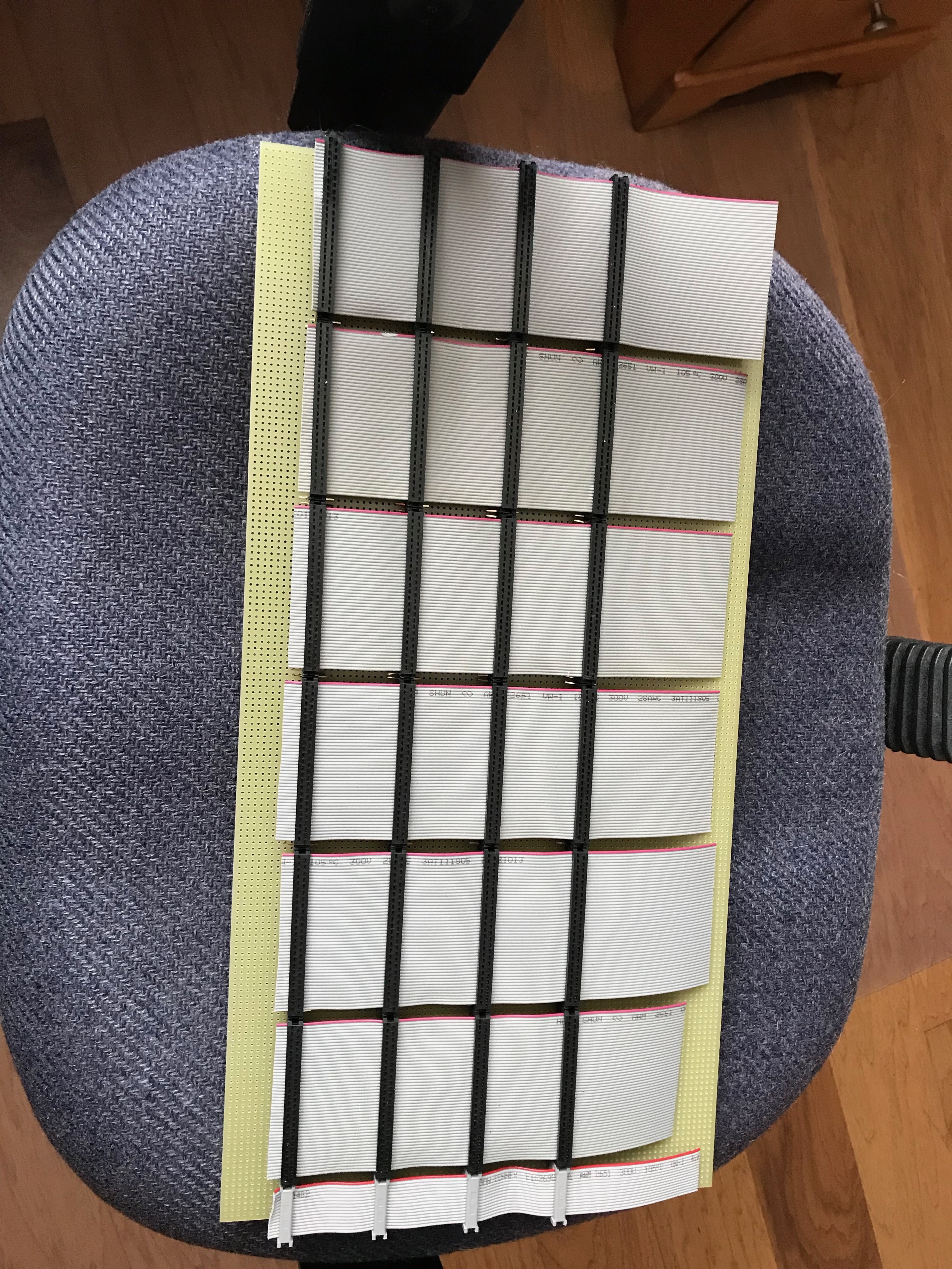
The memory board has been rewired for this new configuration. The control board only had connectors and those have been relocated. The only mod that the display board needs is the power supply connector moved to the other side of the board. You can see that I am working on the breakout board that will connect to the underside of the display board.
Once the breakout board is complete I will connect the memory board to the display board and start the process of re-verifying the wiring to date on the memory board. I stopped wiring the memory board when the realization hit me that without the display board, debugging was getting too hard.
-
Processing Sub-System
07/07/2022 at 12:34 • 0 commentsI have created an initial set of schematics for this sub-system, but have not yet started wiring it up.
Here are design notes that help understand the schematics.
Central Registers: The Central Registers module implement the A, L, Q and Z registers along with implementing the ANDing, ORing and XORing of the A register with the Channel bus. The four central registers have numerous sources of data and various control pulses that perform specific functions. This is all straight forward logic.
The Z register has logic to perform the Z15 and Z16 command pulses. These pulses set the Z register to 040000 and 0100000 respectively.
The WALS command pulse is not simplistic.
Part of the central registers is the logic read from and write to the channel bus. This logic involves ANDing, ORing and XORing the contents of the A register with the bus data. To simplify the design and the chip count, four 74LS181 ALU chips are used. These chips have a 4-bit mode select. The Mode Control is set high to inhibit internal carries. The A data is set to the contents of the A register while the B data is set to the contents of the channel bus. The write to the channel bus is either a straight pass through, A anded with the channel data or A ored with the channel data. The read from the channel bus also can perform an xor of the data. Note that the instruction indicators are logic low. The following table defines the operations and the mode control values.
Function S0 S1 S2 S3 WRITE L H L H WAND H H L H WOR L H H H READ L H L H RAND H H L H ROR L H H H RXOR L H H L WS0 = !WAND
WS2 = !WOR
WS1 = WS3 = High
RS0 = !RAND
RS1 = High
RS2 = !ROR + !RXOR
RS3 = !READ + !RAND + !ROR
Arithmetic Logic Unit: This module is the most complex of the modules requiring the most design effort. The X, Y, U and B registers are implement in this module. There is also a pseudo C register which is simply the 1's compliment of the B register. The X and Y registers have numerous control pulses to load them with various values. The X and Y registers feed four 4-bit adder chips used to add their values. The output of the adders is contained in the U register.
The U register's bit 16 is either the output of the ALUs or the sign bit (bit 15) extended into bit 16 if RUS is asserted.
The end-around carry bit logic is rather complex as the multiply uses 2's compliment arithmetic where everything else in the computer uses 1's compliment arithmetic. The sub-sequences can disable the end-around carry. The end-around carry is disabled during a multiply using the NEACON and NEACOF. This value is stored in a 1-bit register.
The X register has five control pulses that generate six outputs. These include B15X which generates an octal 060000, PONEX which generates an octal 000001, PTWOX which generates an octal 000002, a combination of PONEX and PTWOX which generates an octal 000003, MONEX which generates an octal 177776 and ZERO which zeros the X register. A bit table in MSB first format is as follows.
Pulses Bit Pattern B15X 0100000000000000 PONEX 0000000000000001 PTWOX 0000000000000010 P1X + P2X 0000000000000011 MONEX 1111111111111110 ZERO 0000000000000000 The only bits with any complexity are bits 1 and 2. Their equations are as follows.
1 = !M1X + (P1X + P1X P2X)
2 = M1X + (P2X + P1X P2X)
The U and B registers feed four 4-bit ALU chips that can perform a number of combinational logic sequences. The output of the ALU chips go directly to the Write Bus. The pulses that drive the ALU logic include the RB, RC and RU. The following equations are required and numbered for reference. WB is the Write Bus.
if RC then

	if RA then WB = A + B  (A in WB) 	: 0

	else WB = B				: 1

if RB then WB = B				: 2

if RU then

	if RC then WB = B + U			: 3

	else if RB then WB = B + U		: 4

	else WB = U				: 5
Equation 0 is implemented separately due to the fact that the A value is contained within the Write Bus. The ALU chip has four control bits. The following table identifies the control bits required to implement the equations.
Equation S3 S2 S1 S0 Function 1 0 1 0 1 !B = C 2 1 0 1 0 B 3 0 0 1 0 !B + U 4 0 0 0 1 B + U 5 1 1 1 1 U This can all be translated into a truth table used to define the values of the four ALU control bits. The S0-3 values are defined as a hex value.
RB RC RU S0-3 0 1 0 5 1 0 0 A 0 1 1 2 1 0 1 1 0 0 1 F Using Karnaugh maps, the following equations were generated.
0 = (B !C) + (A !B C)
1 = (A !C) + (!A B C)
2 = (A !B C) + (A B !C)
3 = (!A B C) + (A B !C)
There are three sequence portions that are duplicates and only need to be implemented once. These sequences are (A !B C), (!A B C) and (A B !C).
As if that weren't enough, the ALU implements six control pulses that ORes fixed values on the write bus. These are R1C, R15, R6, RB1, RB2 and RSTRT. The following table shows the values that are associated with each pulse.
Pulse Octal Bits RB1 000001 0000000000000001 RB2 000002 0000000000000010 R6 000006 0000000000000110 R15 000015 0000000000001101 R1C 177776 1111111111111110 RSTRT 004000 0000100000000000 Most of the bits are either 0 or 1 if R1C is asserted. The exceptions are bit 12 which is also 1 if RSTRT is asserted along with bits 1, 2, 3 and 4.
-
Control Sub-System
07/07/2022 at 12:31 • 0 commentsI have drawn initial schematics for this sub-system, but have not started wiring it up.
Here are design notes that help understand the schematics.
Clock: At the heart of the Clock module is a 4 MHz crystal that is divided into four non-overlapping 1 MHz clock signals; CLK1, CLK2, CLK3 and CLK4. This allows the read data to be placed on the bus before the write signals latch the data into the registers. The clock signal can be replaced by a 555 monostable multi-vibrator chip with a variable resistor to provide a slower, variable clock for debugging purposes. The output of these two sources are used to create the two clock pulses.
The two clock signals are generated using two J-K flip-flops. The following table shows the states of the two flip-flops and their meaning. The first flip-flop (FFA) has its J & K inputs tied high, putting that flip-flop into a toggle mode. The Q output of the first flip-flop feeds the J/K input of the second flip-flop (FFB). This puts the second flip-flop into a hold/toggle mode. The Q and !Q outputs of both flip-flops are ANDed together as follows.
FFA Q FFA !Q FFB Q FFB !Q Signal X X CLK1 X X CLK2 X X CLK3 X X CLK4 Scalar: The Scalar module successively divides the first clock pulse in half using six 4-bit counters. Three clock pulses are pulled out of the scalar. The F10 output is a 100 Hz clock pulse used to drive the time counters. The F13 output is a 12.5 Hz clock pulse used in the TPG module. The F17 output is a 0.78125 Hz clock pulse used in the TPG module. These can also be manually generated for debug purposes. Note that a 2.048 mHz crystal is not available, so a 2.0 mHz crystal will be used. This means the real time clock will not be exactly accurate, but close enough.
The first 4-bit counter divides the 1 MHz clock pulse by ten, resulting in a 51.2 kHz clock pulse. The next five 4-bit counters count down and therefore divide the 51.2 pulse by two.
Timing Pulse Generator: This module is a state machine used to sequence through the timing pulses that make up a memory cycle. There are 12 timing pulses plus two additional pulses to perform startup and two pulses to perform debugging. These 16 timing pulses are cycled via a 4-bit counter. Most state changes occur via the clock 1 pulse unless the system is being debugged. In this case there are state change equations that drive the state machine.
The timing pulse generator is driven by CLK1 which is delayed so the write bus can be written to before the TPG changes state.
There are a number of state changes that are numbered and listed below. Note that moving from TP1 through TP12 is performed via the counter which free runs if the CET input is 1.
From State To State Number Equation STBY PWRON TPG_0 !RESET * (!FCLK + F17) PWRON TP1 TPG_1 !FCLK + F13 TP12 TP1 TPG_2 (RUN * !BPHIT) + (!SNI * INST) TP12 STBY TPG_3 SNI + SA TP12 SRLSE TPG_4 BPHIT = (BPEN * ISBP) + (IBPEN * ISRUPT) + (CBPEN * PINC) SRLSE WAIT TPG_5 !STEP WAIT TP1 TPG_6 STEP + RUN The logic driving this implementation depends heavily on the 74LS161 counter chip. There are two inputs that drive the logic. The first one is the PE or NPE pin. When set low, data is loaded from D0-D3. This data sets the next state to TP1. When NPE is set high, the logic is controlled by the CET pin. The CET pin, when set low operations are put on hold. When high, the chip counts once per clock pulse. The following table shows each state and what these pins need to be to move to the next state.
State Current DCBA Next DCBA 012345678 NPE CET Comment STBY 0 0 0 0 0 0 0 0 0xxxxxxxx 1 0 Goto STBY . . 0 0 0 1 1xxxxxxxx 1 1 Goto PWON PWON 0 0 0 1 0 0 0 1 x0xxxxxxx 1 0 Goto PWON . . 0 0 1 0 x1xxxxxxx 1 1 Goto TP1 TP1 0 0 1 0 0 0 1 1 xxxxxxxxx 1 1 Goto TP2 TP2 0 0 1 1 0 1 0 0 xxxxxxxxx 1 1 Goto TP3 TP3 0 1 0 0 0 1 0 1 xxxxxxxxx 1 1 Goto TP4 TP4 0 1 0 1 0 1 1 0 xxxxxxxxx 1 1 Goto TP5 TP5 0 1 1 0 0 1 1 1 xxxxxxxxx 1 1 Goto TP6 TP6 0 1 1 1 1 0 0 0 xxxxxxxxx 1 1 Goto TP7 TP7 1 0 0 0 1 0 0 1 xxxxxxxxx 1 1 Goto TP8 TP8 1 0 0 1 1 0 1 0 xxxxxxxxx 1 1 Goto TP9 TP9 1 0 1 0 1 0 1 1 xxxxxxxxx 1 1 Goto TP10 TP10 1 0 1 1 1 1 0 0 xxxxxxxxx 1 1 Goto TP11 TP11 1 1 0 0 1 1 0 1 xxxxxxxxx 1 1 Goto TP12 TP12 1 1 0 1 1 1 0 1 xxx1xxxxx 0 x Goto STBY . . 0 0 1 0 xx10xxxxx 0 x Goto TP1 . . 1 1 1 0 xx00xxxxx 1 1 Goto SRLSE . . 1 1 1 0 xx101xxxx 1 1 Goto SRLSE (Address Breakpoint) . . 1 1 1 0 xx10x1xxx 1 1 Goto SRLSE (Counter Breakpoint) . . 1 1 1 0 xx10xx1xx 1 1 Goto SRLSE (Interrupt Breakpoint) SRLSE 1 1 1 0 1 1 0 xxxxxxx0x 1 0 Goto SRLSE . . 1 1 1 1 xxxxxxx1x 1 1 Goto WAIT WAIT 1 1 1 1 0 0 1 0 xxxxxxxx1 0 x Goto TP1 . . 1 1 1 1 xxxxxxxx0 1 0 Goto WAIT The equations that need to be implemented to drive the NPE and CET pins is as follows. Note that the equations derive the negative because the zeros are the simplest to implement.
NPE = (WAIT * TPG_6) + (TP12 * TPG_3) + (TP12 * TPG_2 * (!TPG_3 + !TPG_4))
CET = (STBY * !TPG_0) + (PWON * !TPG_1) + (SRLSE * !TPG_5) + (WAIT * !TPG_6
Control Pulse Matrix: This module is divided into three sections; CPM-A, CPM-B and CPM-C. CPM-A uses nine EPROMs to house 72 of the original control pulses defined in the original NASA documentation. I created a 16-bit address to define each of the sub-sequence timing pulse control pulses. There can be up to five control pulses defined for each timing pulse. It should be noted that there were minor mistakes in the CPM definition in the original documentation.
The address for the EPROMs are as follows:
Bit Purpose 1 BR2 2 BR1 3-6 Timing Pulse 7-9 Stage 10 Channel Bit 11-12 Quarter Code 13-15 Op Code 16 Extend Bit Bits 10-16 are identical to what is defined above except for one sub-sequence, PINC. Instead of extending the address, PINC uses an unused code where bits 10-16 are all 1's. The bits are stored and passed around the system as negative logic, i.e. 0 = asserted.
The EPROMs are laid out as a matrix of individual bits, 72 bits per unique address. These bits are inverted, i.e. 1’s complement negative logic. Eight control pulses are defined per EPROM. The first EPROM defines control pulses 1 through 8, the second defines 9-16 and so on until the last EPROM which defines 65-72 control pulses.
Bits EPROM Name 1-8 CPM1_8.hex 9-16 CPM9_16.hex 17-24 CPM17_24.hex 25-32 CPM25_32.hex 33-40 CPM33_40.hex 41-48 CPM41_48.hex 49-56 CPM49_56.hex 57-64 CPM57_64.hex 65-72 CPM65_72.hex It should be noted that the DINC sub-instruction is not implemented. The MOUT, POUT and ZOUT control pulses are only used by DINC, therefore these have been removed from the list and the control pulses have been re-numbered. This gets the count down to 72, which takes the EPROM chip count down by one.
CPM-B takes a few of the control pulses and asserts other, mostly internal control pulses based on the instruction address. These include RSC, WSC, WG, RCH, WCH, RAD and ZIP. The ZIP processing generates WY, RB, RC, WYD, CI and MCRO as follows.
L15 L2 L1 Addr READ WRITE CARRY REMAINDER 0 0 0 0 – WY – – 0 0 1 1 RB WY – – 0 1 0 2 RB WYD – – 0 1 1 3 RC WY CI MCRO 1 0 0 4 RB WY – – 1 0 1 5 RB WYD – – 1 1 0 6 RC WY CI MCRO 1 1 1 7 – WY – MCRO CPM-C asserts control pulses based on the timing pulse of the memory cycle. This drives such things as reading and writing memory values. The state of the TPG cycle drives what control pulses are asserted. The following table is a summary of the control pulses that are asserted for each state and any logic required to assert that pulse. This logic can also be found in the CPM.java code. Some of the more complicated “if” statements are summarized into their own control pulses defined after the table.
State Control Pulses Asserted and Logic STBY assert GENRST PWRON assert NISQ, RSTRT, WZ TP1 if DOTP1 then set CLREXT reg bit, if WS then assert WTS TP3 if STAGE is asserted then assert DCDSUB TP4 if DOTP4 then assert SBWG TP6 if DOTP6 then assert SBWG TP7 if DOTP7 then assert WE TP10 if DOTP10 then assert WE TP11 assert WTS, WPCTR. If sub-sequence = RSM3 then assert CLRP TP12 (see TP12 below) TP12:
if SNI register bit is 1 then
	if IRQ asserted then assert INTR, RPT, INHINT

	else assert RB, WSQ

	assert CLISQ
 if DOTP12 then assert RSTSTG, DCDSUB
 if (runPINC & PreStage reg = 0 & EXT reg = 0) then assert PINC
 if CLREXT register = 1 then clear EXT reg bit & clear CLREXT reg bit
DOTP1 is set if (EXT reg bit = 1 & Stage reg != 2 & subseq != (NDX0/NDX1/NDXX0/NDXX1/DCA0/DCS0/DV0/DV1/DV3/DV7/MP0/MP1/RUPT0))
DOTP4 is set if (GTR7 is asserted & GTR1777 is not asserted & subseq != (DV3/DV7/DV6/DV4))
DOTP6 is set if (GTR1777 is asserted & subseq != (DV3/DV7/DV6/DV4))
DOTP7 is set if (WG/GTR7 are asserted & GTR177 is not asserted & WE is not asserted & subseq != TCF0 or subseq == ADS0/TS0/DAS1)
DOTP10 is set if (GTR7 is asserted & GTR1777 is not asserted & Stage reg != 2 & subseq != TCF0/TC0/BZF0/NDX1/MP1/MP3/RSM3/DV0/DV1/DV3/DV4/DV6/DV7/READ0/WRITE0/RAND0/WAND0/ROR0/WOR0/RXOR0/DXCH0/DXCH1/NDXX1)
DOTP12 is set if (subseq != DV0/DV1/DV3/DV7/DV6)
Notice that some of the signals have a suffix of “a” or “b” or “c”. This designates that more than one chip is asserting that signal. These need to to be ORed together so that there is only one source of the signal.
Sequence Generator: This module contains the staging logic, branching logic, SNI register and Sequence register. In Block I the stage register is two bits. In Block II the stage register was extended to three bits due to the divide instruction. I also needed to add a pre-Stage register to facilitate pre-staging of the divide instruction. I refer to the two registers as the Stage and preStage registers. The next sub-sequence stage is set up using the ST1, ST2 and DVST control pulses. These pulses set the preStage register and during TP12 the preStage register is moved the Stage register using the RSTSTG pulse.
The divide is unique in that it uses the STAGE pulse to increment to the next stage after TP3. The sequence of stages for the divide instruction is not sequentially numeric. It uses a simple routine that implements an inverted end-around carry. The best way to show this is visually. To increment the stage number the bits are shifted left one bit with the end around carry being inverted. This is ingenious because it avoids stage #2 which is reserved for the STD2 sub-sequence, it provides the required 6 sub-sequences and it is easy to implement.
Stage # Bit Pattern 0 000 1 001 3 011 7 111 6 110 4 100 The other interesting aspect of this is that it would normally take six memory cycles to implement the six stages. This was modified such that the DV0 sub-sequence only runs for three timing pulses before the DVST control pulse switches to the next sub-sequence. The next sub-sequence then runs from TP4 through TP12 and then TP1 through TP3. At the end DV4 only has TP4 through TP12 defined. This allows the divide instruction to only take five memory cycles.
The branching register consists of two bits that are set by five test control pulses; TSGU, TSGN, TSGN2, TOV and TPZG. These use simple gate logic to decide if the two branch values should be set. The following equations show how BR1 and BR2 are set. The variables U16, L15 and WB15 indicate the values of those register's bits.
BR1 = (TSGU * U16) + (TL15 * L15) + (TSGN * WB15) + (TOV * WB16)
BR2 = (TSGN2 * WB15) + (TOV * WB15) + (TPZG * GMZ) + (TMZ * WBMZ)
The Sequence Generator decodes the sub-sequence using the opcode, quarter code, channel bit and stage values. To simplify the logic, these are stored in a single EPROM. A number of these sub-sequence values are used throughout the computer to drive logic based on which sub-sequence is running. Some of these values are combined to determine when other internal control pulses should be asserted. The 10-bit input “address” to the EPROM is as follows: EOOOQQCSSS where E = the EXTEND bit, OOO = the 3 bit opcode, QQ = the 2 bit quarter code, C = the channel bit and SSS = the 3 bit stage. The output of the EPROM is a 6-bit number representing the subsequence number defined in the design section.
The instruction decoding address depends on the “don't care” bits of the instruction table shown in the design section being zeroed. The table below lists the bits based on the opcode groups. In code this is an if, else if, else if, else construct.
Index EXT SQ5 SQ4 SQ3 SQ2 SQ1 SQ0 STG3 STG2 STG1 Stage = 2 0 0 0 0 0 0 0 STG3 STG2 STG1 Order = 010 EXT SQ5 SQ4 SQ3 SQ2 SQ1 SQ0 STG3 STG2 STG1 Order = 1, 2, 5, 011, 012, 016 EXT SQ5 SQ4 SQ3 SQ2 SQ1 0 STG3 STG2 STG1 Else EXT SQ5 SQ4 SQ3 0 0 0 STG3 STG2 STG1 The resulting logic is as follows:
The three Stage bits are always the stage value.
The EXT, SQ5, SQ4 & SQ3 bits are their normal values unless the Stage value is 2, then the bits are zeroed.
The SQ0 bit is zero unless the Order code is octal 10.
The SQ1 and SQ2 bits are their true values if the Order code is octal 1, 2, 5, 10, 11, 12 or 16. This last equation is the only one that is not simplistic. If the bits are placed in a truth table (see below) are the values that produce a true, then the following equation is derived. As before, the NOT value is shown as an underline versus an over bar. The NOR is represented as a ||.
Value A B C D 1 0 0 0 1 2 0 0 1 0 5 0 1 0 1 9 1 0 0 1 10 1 0 1 0 14 1 1 1 0 Result = (!A !C D) + (!B !C D) + (!B C !D) + (A C !D) = (!C !D) || (C D) || (!A B !D) || (A B !C)
Sheet CTL_SEQ_CTL has logic that implements the “if” statements of CPM-C. The naming convention is based on the timing pulse the “if” statement is associated with, such as DOTP1 is the “if” construct for timing pulse 1. The “if” statements are shown below.
TP1 = if (EXTEND == 1 & STG != 2 & !NDX0 & !NDX1 & !NDXX0 & !NDXX1 & !DCA0 & !DCS0 & !DV0 & !DV1 & !DV3 & !DV7 & !MP0 & !MP1 & !RUPT0)
TP4 = if (GTR_7 & !GTR_1777 & !DV3 & !DV7 & !DV6 & !DV4)
TP6 = if (GTR_1777 & !DV3 & !DV7 & !DV6 & !DV4)
TP7 = if (WG & GTR_7 & !GTR_1777 & !TCF0 & !WE)
TP10 = if (GTR_7 & !GTR_1777 & !TCF0 & !TC0 & STG != 2 & !BZF0 & !NDX1 & !MP1 & !MP3 & !RSM3 & !DV0 & !DV1 & !DV3 & !DV4 & !DV6 & !DV7 & !READ0 & !WRITE0 & !RAND0 & !WAND0 & !ROR0 & !WOR0 & !RXOR0 & !DXCH0 & !DXCH1 & !NDXX1)
TP12 = if (!DV0 & !DV1 & !DV3 & !DV7 & !DV6)
-
Understanding the computer - Part 2
07/07/2022 at 12:18 • 0 commentsHere are additional details you need to understand including the Control Pulse Matrix and the instructions.
The control pulses are the heart of the system. Each instruction has a sequence of control lines that are activated to cause data to flow through the system. Some of the control pulses have a control number in the control number column. These numbers came from the R-700 documentation. Through testing it was discovered there are a few minor errors in the matrix. I found another version that had the correct control pulses. These errors were in the multiply and divide instructions.
The following table is a combination of design and implementation. It lists each control pulse, where it originates and terminates on the hardware diagrams and what function is performed. The hardware diagram names are sub-system followed by module followed by sub-module. The Active State column can have a value of Low or High meaning the control pulse is active low or high, or values of Pulse meaning it is a pulse such as a clock pulse or a value of Bit meaning the value represents a bit value. Most of the control pulses are active low because many of the TTL chip inputs that are controlled are active low. That and many more of the TTL chips are active low logic. The few control pulses that are active high were chosen to be because that resulted in fewer chips required. Just an FYI, this table formats better on my GitHub wiki page.
Control Line Origin Destination Purpose Cntl # Active State A2X CTL-CPM-A PROC-CRG-AREG, PROC-ALU Copy A1-16 into X1-16 by private line (i.e. not through WL). 1 Low B15X CTL-CPM-A PROC-ALU Set bit 15 of X to 1 2 Low BR1 CTL-SEQ CTL-CPM-A BR1 state n/a Low BR2 CTL-SEQ CTL-CPM-A BR2 state n/a Low CI CTL-CPM-A PROC-ALU Set carry in bit into CI register. Adds 1 to adder value. 3 Low CLXC CTL-CPM-A PROC-ALU Clear X register if BR1=0. Used in Divide. 4 Low CLISQ CTL-CPM-C CTL-SEQ Clear the SNI bit n/a Low CLK1 CTL-CLK All 1 MHz Clock n/a Pulse CLK2 CTL-CLK All 1 MHz Clock n/a Pulse CLK3 CTL-CLK All 1 MHz Clock n/a Pulse CLK4 CTL-CLK All 1 MHz Clock n/a Pulse CLRP CTL-CPM-C MEM-INT Clear RpCell register n/a Low DCDSUB CTL-CPM-C CTL-SEQ Decode Sub-sequence n/a Low DISP CTL-CPM-B DSKY-DSP Write to Channel 10 n/a Low DVST CTL-CPM-A CTL-SEQ Cause Divide staging by complimenting the next higher bit position. Sequence: 0, 1, 3, 7, 6, 4. 5 Low DOTP1 CTL-SEQ CTL-CPM-C Do TP1 commands n/a Low DOTP4 CTL-SEQ CTL-CPM-C Do TP4 commands n/a Low DOTP6 CTL-SEQ CTL-CPM-C Do TP6 commands n/a Low DOTP7 CTL-SEQ CTL-CPM-C Do TP7 commands n/a Low DOTP10 CTL-SEQ CTL-CPM-C Do TP10 commands n/a Low DOTP12 CTL-SEQ CTL-CPM-C Do TP12 commands n/a Low EQU3 MEM-MBF CTL-CPM-B Instruction address = 3 n/a Low EQU4 MEM-MBF CTL-CPM-B Instruction address = 4 n/a Low EQU6 MEM-MBF CTL-CPM-B Instruction address = 6 n/a Low EQU17 MEM-ADR CTL-SEQ Inst. address = 17 n/a Low EXAMNXT MEM-ADR_S MEM-ADR-MDE Examine next key pressed n/a Low EXT CTL-CPM-A, CTL-CPM-B CTL-SEQ-SEQB Set the extend bit. 6 Low EXTEND CTL-SEQ-SEQB CTL-CPM-C, CTL-CPM-A, CTL-SEQ >td >n/a Bit F10X CTL-SCL MEM-CTR-CTL 100 Hz timeout n/a Low F13X CTL-SCL CTL-TPG 12.5 Hz timeout n/a Low F17X CTL-SCL CTL-TPG 0.78125 Hz timeout n/a Low FCLK CTL-MON MEM-ADR-MDE Clock Mode n/a Low GENRST CTL-MON All General Reset n/a Low G1 MEM-MBF PROC-CRG-AREG G reg bit 1 value n/a Bit G16 MEM-MBF PROC-CRG-AREG G reg bit 16 value n/a Bit G2LS CTL-CPM-A PROC-CRG-LREG, MEM-MBF-GMB Copy G16,15-4,1 into L16,12-1 and X15 7 Low GETBP CTL-TPG MEM-ADR-ATS, MEM-ADR-CTL Get Breakpoint Address n/a Low GMZ MEM-MBF-GMB CTL-SEQ-SEQA G reg. is all zeros n/a Low GP MEM-EFM MEM-PAR Generate Parity n/a Low GTR7 MEM-ADR-CTL CTL-CPM-B Address is > 07 n/a Low GTR1777 MEM-ADR-CTL CTL-CPM-B, MEM-EFM Address is > 01777 n/a Low INDC CTL-CPM-B DSKY-DSP Write to channel 11 n/a Low INHINT CTL-CPM-B MEM-INT Execute INHINT command n/a Low INTR CTL-CPM-C CTL-SEQ Perform Interrupt (RUPT) n/a Low IRQ MEM-INT CTL-CPM-C Interrupt requested n/a Low ISBP MEM-ADR-CTL CTL-TPG >td >n/a Low ISRUPT MEM-INT CTL-TPG Is an interrupt pending? n/a Low KB_STR DSKY-KBD MEM-INT Key Strobe, data is latched n/a Low KBD1 CTL-CPM-B DSKY-KBD Read Channel 15 n/a Low KRPT CTL-CPM-A MEM-INT Reset the current RUPT priority (cell). 8 Low L1 PROC-CRG-LREG CTL-CPM-B L register bit 1 value n/a Bit L2 PROC-CRG-LREG CTL-CPM-B L register bit 2 value n/a Bit L15 PROC-CRG-LREG PROC-ALU L register bit 15 value n/a Bit L16 CTL-CPM-A PROC-CRG-LREG Set bit 16 of L to one. 9 Low L2GD CTL-CPM-A MEM-MBF, PROC-CRG-LREG Copy L1-14,16 directly (not through WL) into G2-15,16. Also set G1 bit if MCRO pulse is set. 10 Low MANDATA MEM-ADR-MDE MEM-EFM, MEM-MBF-GMB 0 = AGC (normal ops), 1 = Manual Data n/a Low MCRO CTL-CPM-B MEM-MBF-MBL Part of the ZIP command. n/a Low MONEX CTL-CPM-A PROC-ALU Set bits 2-16 of X to ones, clear bit 1. 11 Low MOUT Only used by DINC, not implemented. N/A Causes generation of one minus drive pulse. n/a Low NEACOF CTL-CPM-A PROC-ALU Permit end around carry after end of MP3. 12 Low NEACON CTL-CPM-A PROC-ALU Inhibit end around carry until NEACOF. 13 Low NISQ CTL-CPM-A, CTL-CPM-C CTL-SEQ Set SNI bit. Next instruction to be loaded into SQ register. Permits increments and interrupts. 14 Low PARALM MEM-PAR DSKY-DSP-IND Parity Alarm n/a High PIFL CTL-CPM-A PROC-ALU Prevents writing into bit 1 of Y reg on a WYD pulse if bit 15 of L reg contains a 1. Used for DV instruction. 15 Low PINC CTL-CPM-C CTL-SEQ Execute PINC command n/a Low PONEX CTL-CPM-A PROC-ALU Clear X register and set bit 1 of X to 1. 16 Low PSTGZ CTL-SEQ-SEQA CTL-CPM-C PreStage is zero. n/a Low PTWOX CTL-CPM-A PROC-ALU Clear X register and set bit 2 of X to 1. 17 Low R15 CTL-CPM-A PROC-ALU Octal 015 to WL's 18 Low R1C CTL-CPM-A PROC-ALU 1’s compliment of octal 1 to write bus (WL's) 19 Low R6 CTL-CPM-A PROC-ALU Octal 6 to WL's 20 Low RA CTL-CPM-A PROC-CRG-AREG Read A1-16 to WL1-16. 21 Low RAD CTL-CPM-A CTL-CPM-B Read address of next instruction. Appears at TP8 and normally interpreted as RG. If next instruction is INHINT, RELINT or EXTEND, it is interpreted as RZ & ST2 instead. 22 Low RB CTL-CPM-A, CTL-CPM-C PROC-ALU Read B1-16 to WL1-16 23 Low RBBK CTL-CPM-A MEM-ADR-BNK Read BB register onto WL's. FB16 to WL16,15 & FB11-14 to WL11=14 & EB9-11 to WL1-3. 27 Low RB1 CTL-CPM-A PROC-ALU Octal 1 onto WL's 24 Low RB1F CTL-CPM-A PROC-ALU Octal 1 onto WL's if BR1=1. 25 Low RB2 CTL-CPM-A PROC-ALU Octal 2 onto WL's 26 Low RC CTL-CPM-A PROC-ALU Read C register (B') 28 Low RCH CTL-CPM-A CTL-CPM-B, PROC-CRG-RCHN, MEM-ADR-ATS Read contents of channel address in S. Channel bits 1-14 to WL1-14 & bit 16 to WL15,16. Channels 1 & 2 same as RL and RQ 29 Low REB CTL-CPM-B MEM-ADR-BNK Read erasable bank reg n/a Low RELINT CTL-CPM-B MEM-INT Execute RELINT command. n/a Low RFB CTL-CPM-B MEM-ADR-BNK Read fixed bank reg n/a Low RG CTL-CPM-A, CTL-CPM-B MEM-MBF Read G1-16 onto WL1-16. 30 Low RL CTL-CPM-A PROC-CRG-LREG Read L1-14 to WL1-14 and L16 to WL15,16 31 Low RLC CTL-CPM-B PROC-CRG-LREG Read channel bus into L register n/a Low RL10BB CTL-CPM-A PROC-ALU Read B1-10 to WL1-10. Replaces c(S) by a 10 bit address. 32 Low RPRO CTL-CPM-A DSKY-KBD Read the PRO key from DSKY. n/a High RPT CTL-CPM-C MEM-INT Latch Interrupt Vector n/a Low RQ CTL-CPM-A PROC-CRG-QREG Read Q1-16 to WL1-16 33 Low RQC CTL-CPM-B PROC-CRG-QREG Read Channel bus into Q register n/a Low RRPA CTL-CPM-A MEM-INT Read address of highest priority interrupt requested. 34 Low RSB CTL-CPM-B MEM-ADR-BNK Read Channel 7 n/a Low RSC CTL-CPM-A CTL-CPM-B Read central register defined by address in S reg. Bits 1-16 to WL1-16. 35 Low RSCT CTL-CPM-A MEM-CTR-CNT Read address of highest priority counter request. 36 Low RSM3 CTL-CPM-A CTL-CPM-C Subsequence RSM3 is active. (output to C only, not outside CPM) n/a Low RSTRT CTL-CPM-A, CTL-CPM-C PROC-ALU Octal 04000 to WL's. Block 2 start address. 37 Low RSTSTG CTL-CPM-A, CTL-CPM-C CTL-SEQ Reset the stage counter to zero. 38 Low RU CTL-CPM-A PROC-ALU Read U1-16 to WL1-16 39 Low runPINC MEM-CTR-CNT CTL-CPM-C Run the PINC sub-seq. n/a Low RUS CTL-CPM-A PROC-ALU Read U1-14 to WL1-14 & U15 to WL15,16 40 Low RZ CTL-CPM-A, CTL-CPM-B PROC-CRG-ZREG Read Z1-16 to WL1-16 41 Low SBWG CTL-CPM-C MEM-EFM, MEM-MBF-MBL Write G register to memory shifted. n/a Low SNI CTL-SEQ CTL-CPM-C, CTL-TPG Set up for next instruction. n/a Low STBY CTL-TPG Various Put AGC in standby by; disable display, n/a Low ST1 CTL-CPM-A CTL-SEQ Set Stage 1 flip flop to 1 at next TP12. 42 Low ST2 CTL-CPM-A, CTL-CPM-B CTL-SEQ Set Stage 2 flip flop to 1 at next TP12. 43 Low STAGE CTL-CPM-A CTL-SEQ, CTL-CPM-C, CTL-SEQ Execute next sub-instruction as defined by stage counter. 44 Low TL15 CTL-CPM-A CTL-SEQ Copy L15 into BR1. 45 Low TM3RUPT MEM-CTR-CTL MEM-INT Interrupt 3 asserted n/a Low TM4RUPT MEM-CTR-CTL MEM-INT Interrupt 4 asserted n/a Low TMZ CTL-CPM-A CTL-SEQ Test WL1-16 for all ones. Set BR2=1 if true, else BR2=0. 46 Low TOV CTL-CPM-A CTL-SEQ Test for overflow (WL16,15). Set BR1/BR2 to 00 if no overflow, 01 if positive overflow, 10 if negative overflow. 47 Low TP MEM-EFM MEM-PAR Test Parity n/a Low TPZG CTL-CPM-A CTL-SEQ Test content of G for +0. If true, set BR2 to 1, else BR2=0. 48 Low TRSM CTL-CPM-A CTL-SEQ Test for resume address (0017) during NDX0. If exists, set c(ST)=3 to execute RSM3, else set c(ST)=1. 49 Low TSGN CTL-CPM-A CTL-SEQ Test Sign. Copy WL16 to BR1. 50 Low TSGN2 CTL-CPM-A CTL-SEQ Test Sign 2. Copy WL16 to BR2. 51 Low TSGU CTL-CPM-A CTL-SEQ Test sign of Sum (U16). Copy U16 into BR1. 52 Low U16 PROC-ALU PROC-CRG-AREG U reg bit 16 value n/a Bit U2BBK Only used by FETCH1, not implemented. N/A Adder bits U16,14-11 to FB and U1-3 to EB1-3. May be inhibited by signal MONWBK. 53 Low W20 CTL-CPM-B MEM-MBF-MBL, MEM-MBF-SFT Perform CYR n/a Low W21 CTL-CPM-B MEM-MBF-MBL, MEM-MBF-SFT Perform SR n/a Low W22 CTL-CPM-B MEM-MBF-MBL, MEM-MBF-SFT Perform CYL n/a Low W23 CTL-CPM-B MEM-MBF-MBL, MEM-MBF-SFT Perform EDOP n/a Low WA CTL-CPM-A PROC-CRG-AREG Clear and write WL1-16 into A1-16. 54 Low WALS CTL-CPM-A PROC-CRG-AREG, PROC-CRG-LREG Clear and write into A1-14 from WL3-16. If G1=0, then G16 to A15,16, else U16 to A15,16. Clear and write WL1-2 to L13-14. 55 Low WB CTL-CPM-A PROC-ALU Clear and write from WL1-16 into B1-16. 56 Low WBB CTL-CPM-B MEM-ADR-BNK Write to both banks n/a Low WCH CTL-CPM-A CTL-CPM-B, PROC-CRG-WCHN Clear and write W1-14,16,parity into channel bits 1-14,16,parity. Channel address in S reg. Channels 1 & 2 same as WL & WQ. 57 Low WE CTL-CPM-C MEM-EFM, MEM-MBF-MBL Write G register contents into memory based on S address. n/a Low WEB CTL-CPM-B MEM-ADR-BNK Write to Erasable Bank n/a Low WFB CTL-CPM-B MEM-ADR-BNK Write to Fixed Bank n/a Low WG CTL-CPM-A MEM-MBF-SFT, CTL-CPM-B Clear and write WL1-16 into G1-16 except for addresses 020-023 which causes editing. 58 Low WL CTL-CPM-A PROC-CRG-LREG Clear and write WL1-16 into L1-16. 59 Low WLC CTL-CPM-B PROC-CRG-LREG Write L register to channel bus n/a Low WOVR CTL-CPM-A MEM-CTR-CTL Test WL15,16 for positive overflow. If S contains 0025, increment counter 024. If S contains 026, 027 or 030 then execute RUPT. 60 Low WPCTR CTL-CPM-C MEM-CTR-CNT Increment counter n/a Low WQ CTL-CPM-A PROC-CRG-QREG Clear and write WL1-16 into Q1-16. 61 Low WQC CTL-CPM-B PROC-CRG-QREG Write to Q register to channel bus n/a Low WS CTL-CPM-A MEM-ADR-S, CTL-CPM-C Clear and write WL1-12 into preS1-12. 62 Low WSB CTL-CPM-B MEM-ADR-BNK Write to Channel 7 n/a Low WSC CTL-CPM-A CTL-CPM-B Clear and write into central register specified by S register 63 Low WST CTL-CPM-C MEM-ADR-S Move preS data to S reg n/a Low WSQ CTL-CPM-A, CTL-CPM-C CTL-SEQ Clear and write WL10-14,16 into SQ10-14,16 and copy extend flop flop into SQ15. 64 Low WY CTL-CPM-A PROC-ALU Clear X, Y & CI. Write WL1-16 into Y1-16. 65 Low WY12 CTL-CPM-A PROC-ALU Clear X, Y & CI. Write WL1-12 into Y1-12. 66 Low WYD CTL-CPM-A PROC-ALU Clear X, Y & CI. Write WL1-14 into Y2-15 and WL16 into Y16. Write WL16 into Y1 except 1) when end-around carry is inhibited by NEACON 2) during SHINC sequence or 3) PIFL is active and L15=1. 67 Low WZ CTL-CPM-A, CTL-CPM-C PROC-CRG-ZREG Clear and write WL1-16 into Z1-16. 68 Low Z15 CTL-CPM-A PROC-CRG-ZREG Set bit 15 of Z to 1. 69 Low Z16 CTL-CPM-A PROC-CRG-ZREG Set bit 16 of Z to 1. 70 Low ZAP CTL-CPM-A CTL-CPM-A Generate control pulses RU, G2LS & WALS. Used by MP K instruction. 71 Low ZIP CTL-CPM-A CTL-CPM-A Generate control pulses A2X & L2GD. Also the pulses shown below. 72 Low ZIP also implies if L15,2,1 are:
L15 L2 L1 READ WRITE CARRY REMAINDER 0 0 0 – WY – – 0 0 1 RB WY – – 0 1 0 RB WYD – – 0 1 1 RC WY CI MCRO 1 0 0 RB WY – – 1 0 1 RB WYD – – 1 1 0 RC WY CI MCRO 1 1 1 – WY – MCRO The instructions that are executed by the AGC are integral to the understanding of both the hardware and the software. They are described here so as not to clutter the design section. In the following sections, L is the location of the instruction and K is the data address (i.e. the operand) of the instruction. Items in parenthesis preceded by “c” mean the resulting contents of that variable. Items in parenthesis preceded by “b” mean the contents before the operations. The “editing if K is 0020 – 0023” means the bit shifts and rotates occur.
There are both “voluntary” and “involuntary” instructions. The voluntary instructions are the ones that can be coded, compiled and placed in fixed memory to execute. The involuntary instructions are triggered as part of counter interrupts and cannot be coded into a fixed memory program. The only involuntary instruction implemented here is the PINC instruction due to the limited counters implemented.
- TC K: Transfer Control
This instruction transfers control to address K after placing the return address into Q. The special cases are K = 3, 4 & 6.
c(Q) ← L + 1
- TC 3: RELINT: Allow Interrupts
This instruction allows the resumption of interrupts after the INHINT instruction.
- TC 4: INHINT: Inhibit Interrupts
This instruction inhibits interrupts from occurring.
- TC 6: EXTEND: Extracode Bit
This instruction sets the extracode bit which sets the high order, bit 16 of the opcode. This is used to double the number of available instructions and is used for less frequently used instructions as it requires this extra instruction to execute the extracode instructions.
- CCS K: Count, Compare & Skip
This instruction is a four way branching instruction. The following describes the four branching conditions. The value assigned to K is called the Diminished Absolute Value (DABS) which replaces A with one less than the its previous value. This allows for a looping count down construct.
c(A) ← DABS[(K)] where DABS(x) = |x| - 1 if |x| > 1 or +0 if |x| <= 1
c(K) ← b(K), editing if K is 0020 - 0023
if b(K) > +0 then no skip
if b(K) = +0 then skip to L + 2
if b(K) < -0 then skip to L + 3
if b(K) = -0 then skip to L + 4
- DAS K: Double Add to Storage
This instruction adds the contents of K and K + 1 to the A and L registers. If K or K + 1 is 0020 through 0023 then the shifts/rotates occur.
c(K, K + 1) ← b(A, L) + b(K, K + 1)
- LXCH K: Exchange L and K
This instruction exchanges L with K. The prime tick indicates overflow correction.
c(L) ← b'(K)
c(K) ← b(L), editing if K is 0020 - 0023
- INCR K: Increment
This instruction increments K.
c(K) ← b(K) + 1, editing if K is 0020 - 0023
- ADS K: Add to Storage
This instruction adds A to K and the results are both placed into A and K.
c(A) & c(K) ← b(K) + b(A), editing if K is 0020 - 0023
- CA K: Clear and Add
This instruction places the value of K into A.
c(A) ← b(K)
c(K) ← b(K), editing if K is 0020 – 0023
- CS K: Clear and Subtract
This instruction places the negated value of K into register A.
c(A) ← -b(K)
c(K) ← b(K), editing if K is 0020 - 0023
- INDEX K: Index Next Instruction
This instruction modifies the next instruction by adding the operand to the next instruction.
c(K) ← b(K), editing if K is 0020 – 0023
Use [b(K) + c(I + 1)] as next instruction
- INDEX 0017: Resume Interrupted Program
This is a special instruction that resumes from an interrupted program. c(0017) contains the next instruction.
c(Z) = c(0015)
- DXCH K: Double Exchange
This instruction exchanges the contents of A and L with K and K + 1.
c(A, L) ← b(K, K + 1)
c(K, K + 1) ← b(A, L), editing if K or K + 1 is 0020 - 0023
- TS K: Transfer to Storage
This instruction transfers the contents of K to storage.
c(K) ← b(A), editing if K is 0020 - 0023
if (A) has positive overflow, A ← +1, skip to L + 2
if (A) has negative overflow, A ← -1, skip to L + 2
- XCH K: Exchange
This instruction exchanges the data in K with the data in register A.
c(A) ← b(K)
c(K) ← b(A), editing if K is 0020 - 0023
- MASK K: Mask
This instruction ORs the contents of K with the contents of A.
c(A) ← b(A) || c(K)
- READ KC: Read Channel KC
This instruction reads the KC channel into register A.
c(A) ← c(KC)
- WRITE KC: Write Channel KC
This instruction writes the contents of register A onto the KC channel.
c(KC) ← c(A)
- RAND KC: Read and Mask
This instruction reads the KC channel and ANDs it with the contents of register A.
c(A) ← b(A) & c(KC)
- WAND KC: Write and Mask
This instruction writes the contents of register A masked with the contents of KC channel into A and KC.
c(KC) and c(A) ← b(A) & b(KC)
- ROR KC: Read and Superimpose
This instruction reads the KC channel and ORes it with the contents of register A.
c(A) ← b(A) || c(KC)
- WOR KC: Write and Superimpose
This instruction writes the contents of register A ORed with the contents of KC channel into A and KC.
c(KC) and c(A) ← b(A) || b(KC)
- RXOR KC: Read and Invert
This instruction reads the KC channel and XORes it with the contents of register A.
c(A) ← b(A) xor c(KC)
- DV K: Divide
This instruction divides the contents of A by the contents of K. The quotient is placed in A and the remainder is places in Q.
c(A) ← b(A, L) / c(K)
c(L) ← remainder
- **BZF K: Branch Zero to Fixed ** This instruction branches to instruction in K if the contents of A is zero else it simply executes the next instruction.
If c(A) = 0 then branch to K.
- MSU K: Modular Subtract
This instruction performs a 1's compliment subtraction of K from A. A modular subtraction is the difference between two unsigned 2's compliment inputs.
c(A) ← b(A) 0 b(K) where 0 is a modular subtract
c(K) ← b(K), editing if K is 0020 – 0023
- QXCH K: Exchange Q and K
This instruction exchanges the contents of the Q register and the contents of K.
c(Q) ← b(K)
c(K) ← b(Q), editing if K is 0020 – 0023
- AUG K: Augment
This instruction augments K which means the value is incremented if positive or decremented if negative.
If b(K) >= +0, c(K) ← b(K) + 1, editing if K is 0020 – 0023
If b(K) <= -0, c(K) ← b(K) - 1, editing if K is 0020 – 0023
- DIM K: Diminish
This instruction diminishes K which means the value is decremented if positive or incremented if negative.
If b(K) > +0, c(K) ← b(K) - 1, editing if K is 0020 – 0023
if b(K) = 0, c(K) ← b(K), editing if K is 0020 - 0023
If b(K) < -0, c(K) ← b(K) +1, editing if K is 0020 – 0023
- DCA K: Double Clear and Add
This instruction moves K and K + 1 to A and L.
c(A, L) ← b(K, K + 1)
c(K) ← b(K), editing if K is 0020 – 0023
c(K + 1) ← b(K + 1), editing if K is 0020 – 0023
- DCS K: Double Clear and Subtract
This instruction moves the negated values of K and K + 1 to A and L.
c(A, L) ← -b(K, K + 1)
c(K) ← b(K), editing if K is 0020 – 0023
c(K + 1) ← b(K + 1), editing if K is 0020 – 0023
- INDEX K: Index Extracode
This instruction is the same as the non-extracode version except the extracode switch is not reset.
- SU K: Subtract
This instruction subtracts the contents of K from A. If an overflow occurs, either +1 or -1 is placed into A depending on the type of overflow.
c(A) ← b(A) – b(K)
c(K) ← b(K), editing if K is 0020 – 0022
- BZMF K: Branch Zero or Minus to Fixed
This instruction branches to the instruction at K if register A is zero or negative, otherwise it continues with the next instruction.
if c(A) <= +0, branch to instruction at K,
else execute next instruction
- MP K: Multiply
This instruction multiplies the contents of with the contents of K. The results are placed into the A and L registers.
c(A, L) ← b(A) * c(K)
- PINC: Positive Increment
This involuntary instruction is used to increment a counter by one.
c(CTR) = b(CTR) + 1
-
Memory Sub-System
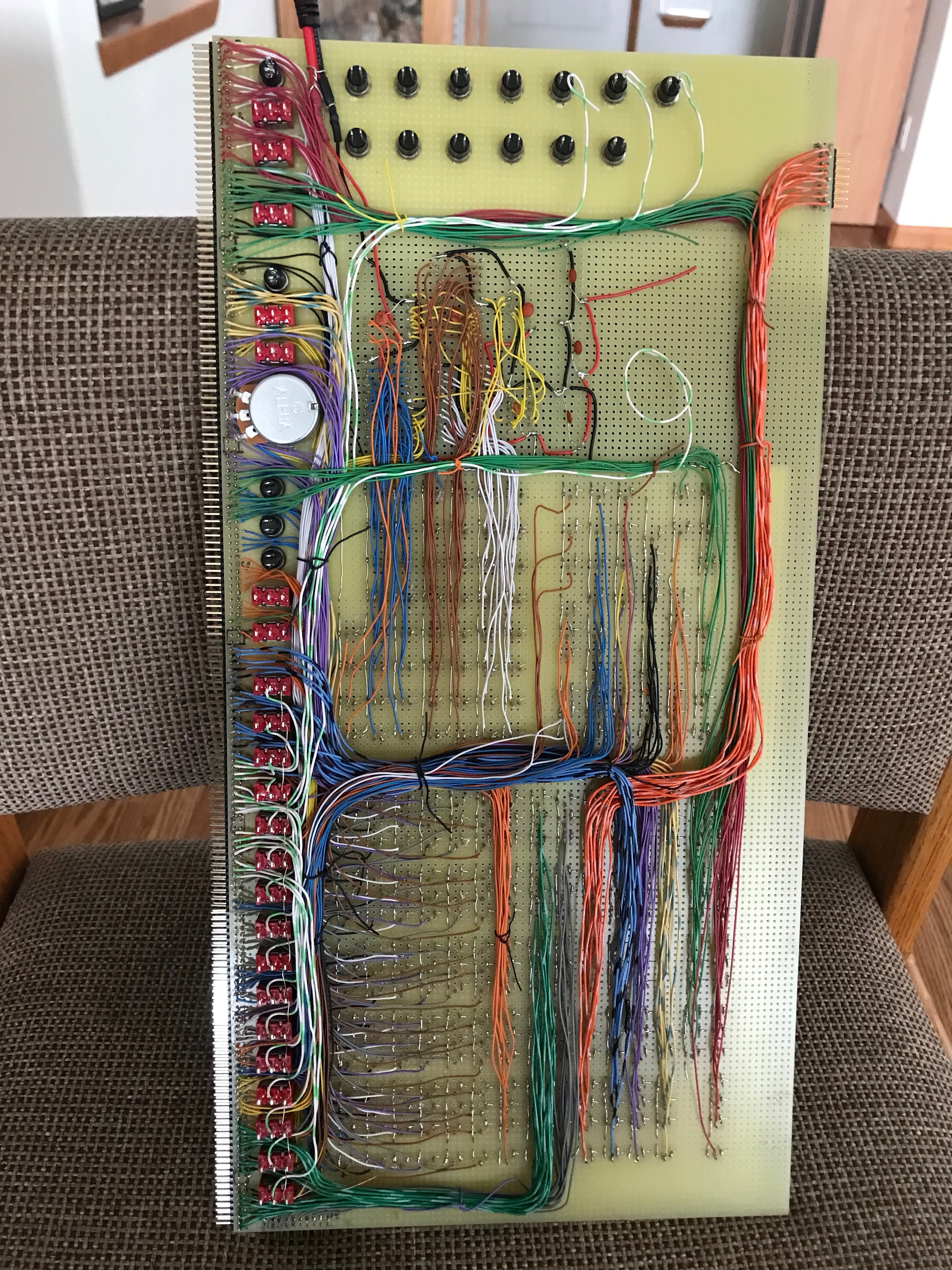
07/06/2022 at 23:54 • 0 commentsThis is where I started. I added the code EPROM and RAM, then started adding various access registers before I became overwhelmed using just my simple 16-bit register viewed. I realized I needed the Display sub-system so I switched gears and have been working on that. Here are some pictures of where I am to date.
![]()
![]()
Even though I have the AGC Code EPROM plugged in, I will probably start with some simpler test programs I have created to test various commands that never seemed to come up in the AGC code. Some of that code contains the more complicated multiply and divide instructions. The documentation has good test case scenarios that I used to make sure they are working.
Here are some design notes that help understand the schematics.
Erasable/Fixed Memory: This module contains a single EPROM chip that contain the code which was generated using the modified assembler. This is a 16-bit data by 16-bit address chip that can handle all the code in the Luminary 099 program. There are also two RAM chips that implement the erasable memory.
The single 16-bit EPROM brings some simplification from a chip count, however it is more complicated from an implementation standpoint. The data lines are a bit reversed from what you might expect. The bytes are reversed and I did not attempt to change this as it is easier to read and verify in this configuration. From a hardware perspective, it is a simple matter to switch the byte's data lines. If the address is 0 then the first data word is 1687 hex. Given this, the data lines are as follows.
1 = D7 – D4
6 = D3 – D0
8 = D15 – D12
7 = D11 – D8
The address lines are as you would expect when dealing with the EPROM. For instance, address 4000 octal equals 800 hex which will give a data value of 0004 hex. The S-Record format is what is a bit strange. The data is defined a byte at a time. To see this data value in the S-Record file, double the address value. In the case of 4000, double 800 hex gives a value of 1000 hex. Looking at the S-Record values at this location you will see 00 04 38 2c.
Memory Buffer: This module encapsulates the G register. All data in and out of memory go through this register. The shifting when writing to addresses 20, 21, 22 and 23 occur in this module. Data arrives via the Write Bus and Direct Write Bus. The data read from fixed memory is checked for specific values; all zeros or GMZ, EQ3, EQ4 and EQ6. The EQ pulses check for the TC instructions that translate into the RELINT, INHINT and EXTEND instructions.
The determination of the four specific G register values results are straight forward except the combination of the CYR and SR. All the bits are the same except bits 14, 15 & 16. The table below shows the values.
Bit W20 W21 Equation 14 B15 B16 (!W21 * B16) + (!W20 * B15) 15 1 0 W21 16 0 B16 (!W21 * B16) Parity: This module in Block I was driven by control pulses within the Control Pulse Matrix. In Block II they realized you always generate parity when writing to memory and test parity when reading from memory. I kept the control pulses as internal pulses to drive this functionality. I chose to implement parity for the erasable ROM memory, but not for the fixed memory. It would be easy enough to implement this if you wanted to.
This functionality is implemented using two parity generator chips. This module contains the P register and PALM (parity alarm) single bit register.
Interrupts: This module implements three of the interrupts; the keyboard interrupt along with TIME3 and TIME4. The inhibit interrupts is also implemented in this module. A RPCell register maintains which interrupt has occurred. When an interrupt is processed, this module converts the specific interrupt into the memory address of the code's interrupt jump table. The address equals 04000 + RUPT # << 2. The addresses are (in octal).
4014 = RUPT3(TIME3)
4020 = RUPT4 (TIME4)
4024 = RUPT5 (KBD
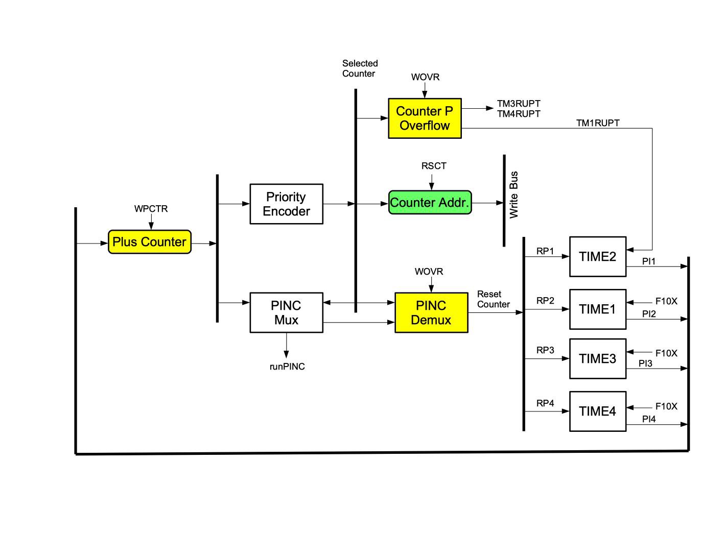
Counters: This module implements four of the counters. The implemented counters and their octal addresses are as follows.
TIME2 = 24
TIME1 = 25
TIME3 = 26
TIME4 = 27
When counters TIME3 and TIME4 overflow, they generate an interrupt. When counter TIME1 overflows, it increments the TIME2 counter. The TIME2 counter should never overflow.
A counter address is generated when asked for by the RSCT control pulse. This is the address of the counter to increment (shown above).
-
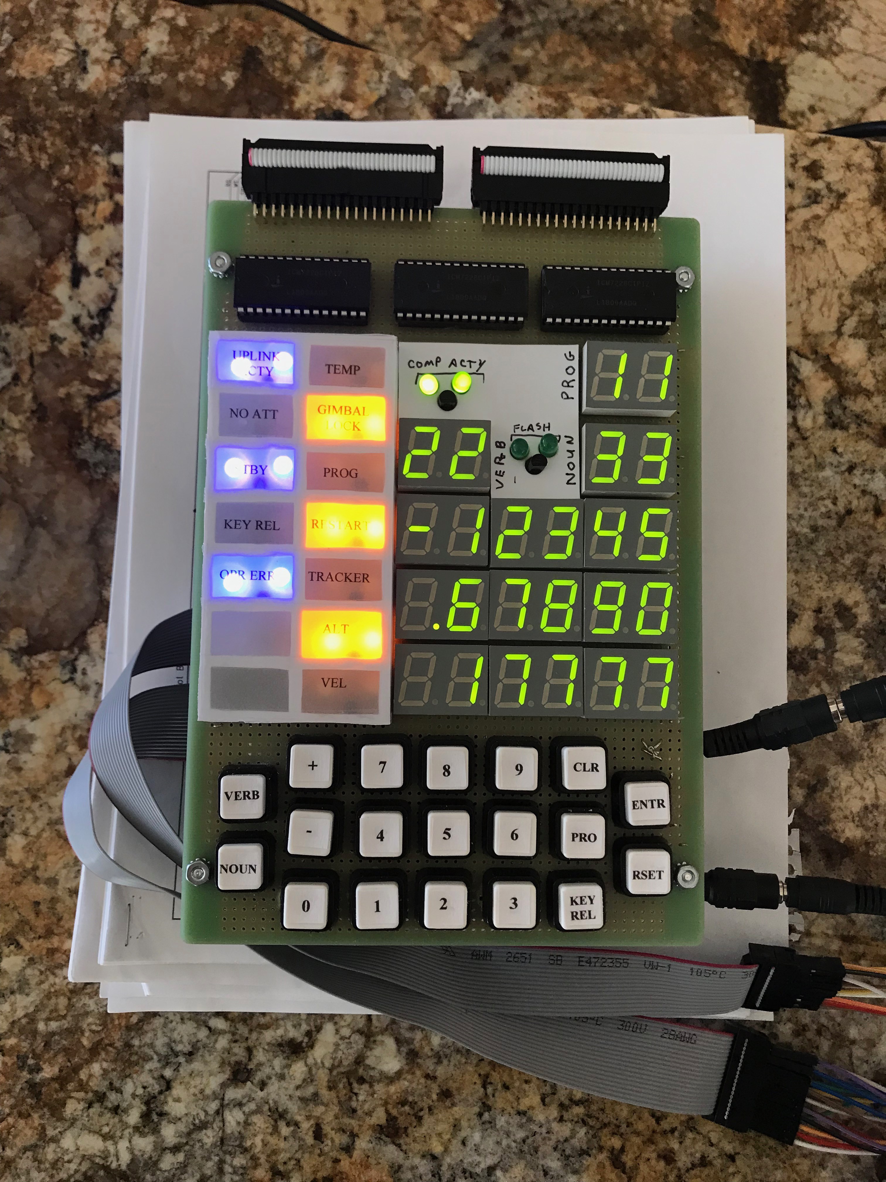
Display
07/06/2022 at 23:47 • 0 commentsI started wiring up the Memory sub-system board and realized quickly that I needed the display board to show the state of the various registers. I first had to create a backplane to connect the boards into. The backplane carries all the signals the display board requires. The display functionality was not part of the original AGC. This functionality is based on my simulator and what I needed to control the simulation. The actual computer required data and control signals are routed via ribbon cables on top of the boards.
Here is the backplane. Notice that I left room for an additional board, just in case. I had to make all the connector cables and slots universal so I could move the board under test to the back of the stack to have access to the wire wrap pins for debugging purposes.
![]()
![]()
The display panel has LEDs grouped by register. In the middle of the board is an array of sub-sequences showing which sub-sequence is being executed. All of the controls that are available on the simulator are available here, including a row of 16 data/address input switches. I chose to solder this board and the front board of the DSKY. All remaining boards are wire wrap for easy modification when I make that inevitable mistake.
![]()
![]()
All the LEDs are wired up and tested. I am working on the switch logic.
Here are some of design notes that help understand the schematics.
The backplane is used to route all LED and switch lines between the logic boards and the display board. There are 338 connectors (169 * 2). If a NOT gate is required for the LED to show positive logic, then that is placed on the logic board.
The lines are laid out so that each of the three logic boards (CTL, MEM, PROC) do not have doubled up or overlapping pins. This way only one row of wire wrap terminals are required. It also strengthens the connection as more pins are anchoring the boards. The schematics use global labels to identify connections to the backplane due to the limitations of drawing real estate. The backplane connectors are shown on the interface drawings as single row connectors. The largest connector is 40 pins so multiple 40 pin connectors are required. The global labels on the hardware diagrams are numbered as per the list below.
The pin layouts identify two rows; A & B. The purpose column identifies the subsystem-module purpose with the number of connections in parenthesis. Note: The register and memory switch LSBs are the lower number, the higher number is the MSB. There are two unused pins every 25 pins due to the space required for the backplane ribbon cable connectors. The following tables shows the pin assignments.
Row A:
Pin # Purpose 1-16 MEM-EFM: Memory Bus (1-16) 17-25 MEM-ADR: S Monitor Bus (1-9) 26-27 Unusable 28-30 MEM-ADR: S Monitor Bus (10-12) 31-39 MEM-ADR: Bank Monitor (9) 40-52 MEM-ADR: Address Bus (1-13) 53-54 Unusable 55-57 MEM-ADR: Address Bus (14-16) 58 MEM-MBF: EQU3 59 MEM-MBF: EQU4 60 MEM-MBF: EQU6 61 MEM-ADR: EQU17 62 MEM-ADR: GTR7 63 MEM-ADR: GTR1777 64 MEM-MBF: GMZ 65 MEM-CTR: INC TIME1 (1) 66 MEM-CTR: INC TIME2 (1) 67 MEM-CTR: INC TIME3 (1) 68 MEM-CTR: INC TIME4 (1) 69 MEM-ADR: Examine Memory Pushbutton (1) 70 MEM-ADR: Examine Next Pushbutton (1) 71 MEM-EFM: Read/Write Switch (1) 72 MEM-ADR: AGC/Manual Switch (1) 73 MEM-ADR: Clear Parity Pushbutton (1) 74 MEM-EFM: Load Memory Pushbutton (1) 75 MEM-INT: RUPT3 Switch (1) 76 MEM-INT: RUPT4 Switch (1) 77 MEM-INT: RUPT5 Switch (1) 78 MEM-PAR: PR_1-15 (1) 79 CTL-MON: SA (1) 80-81 Unusable 82-97 MEM-MBF: G Monitor Bus (1-16) 98-106 MEM-ADR: Memory Switches (1-9) 107-108 Unusable 109-115 MEM-ADR: Memory Switches (10-16) 116 CTL-MON: BPEN (1) 117 CTL-CLK: Clock Control: 1 MHz / Slow (1) 118 CTL-TPG: IBPEN (1) 119 CTL-CLK: CLK1 (1) 120 CTL-TPG: CBPEN (1) 121 CTL-MON: RUN – Exec. Mode (Run/Step) (1) 122 CTL-MON: INST – Exec. Control (Instruction/Sequence) (1) 123 CTL-MON: FLCK – Clock Mode (Run/Step) (1) 124 CTL-MON: Master Reset Switch (1) 125 CTL-MON: STEP – Exec. Step (1) 126 CTL-MON: MCLK – Clock Step (1) 127 CTL-MON: GENRST - Master Reset (1) 128 CTL-MON: Scalar Enable (1) 129-133 CTL-SEQ-SEQB: SQ(0-5) (1-5) 134-135 Unusable 136 CTL-SEQ-SEQB: SQ(0-5) (6) 137 CTL-SEQ-SEQB: SNI (1) 138-140 CTL-SEQ-SEQA: PRE-STG(1-3) (3) 141-143 CTL-SEQ-SEQA: STG(1-3) (3) 144 CTL-SEQ-SEQA: BR1 (1) 145 CTL-SEQ-SEQA: BR2 (1) 146-151 CTL-SEQ_DCD: Sub-Sequence Bus (6) 152-160 CTL-TPG: TPG Decoded State (1-9) 161-162 Unusable 163-169 CTL-TPG: TPG Decoded State (10-16) Row B:
Pin # Purpose 1-16 PROC-ALU: X Monitor Bus (16) 17-25 PROC-ALU: Y Monitor Bus (1-9) 26-27 Unusable 28-34 PROC-ALU: Y Monitor Bus (10-16) 35-50 PROC-ALU: B Monitor Bus (16) 51-52 PROC-ALU: U Monitor Bus (1-2) 53-54 Unusable 55-68 PROC-ALU: U Monitor Bus (3-16) 69-79 PROC-CRG: A Monitor Bus (1-11) 80-81 Unusable 82-86 PROC-CRG: A Monitor Bus (12-16) 87-102 PROC-CRG: L Monitor Bus (16) 103 PROC-ALU: CI (1) 104 CTL-SCL: F10x Switch (1) 105 CTL-SCL: F13x Switch (1) 106 CTL-SCL: F17x Switch (1) 107-108 Unusable 109 CTL-CPMC: PINC (1) 110 CTL-CLK: Clock Rate (1) 111 CTL-SCL: F10x (1) 112 CTL-SCL: F13x (1) 113 CTL-SCL: F17x (1) 114-129 PROC-CRG: Q Mon Bus (1-16) 130-133 PROC-CRG: Z Mon Bus (1-4) – Used by MEM-ADR-ATS 134-135 Unusable 136-147 PROC-CRG: Z Mon Bus (5-16) – Used by MEM-ADR-ATS 148 MEM-PAR: PARALM (1) 149-151 MEM-INT: Selected RUPT (3) 152-154 MEM-INT: RUPT Latch (3) 155 MEM-INT: IRQ (1) 156-159 MEM-CNT: Plus In (4) 160 MEM-CNT: Plus In Sync (1) 161-162 Unusable 163-165 MEM-CNT: Plus In Sync (2-4) 166-168 MEM-CNT: Selected Counter (3) 169 MEM-INT: INH (1) The backplane has enough room in case another chip board is required. No reason to "cut" myself or the ribbon cables short. Here are pictures of the front and back of the board.
CPU Connectors: The J connectors contain the computer connections related to bus data and control pulses. They are designed in such a way that the three rear sub-system boards are interchangeable. This is due to the fact that the “board under test” is in the rear and is easily accessible. This is accomplished by having a connector for each of the slot's ribbon cables on the backplane even though they may not be used by that specific logic board. These connectors are located on the top of the boards. Only two of the ribbon cables extend to the DISP board. These are located on the side of the boards.
The top connections are positioned to the left of the boards. The order is J107, J101, J106, J105, J102 and J100. J107 starts one pin to the right of the edge and there are two unused pins between connectors so the connector cables can fit.
The following table is as summary of the connectors, how many pins, the purpose, the boards requiring the connection and the spares. The pin assignments are left to right for top pins and bottom to top for side assignments.
Label Pins Purpose Boards Spare Pins J100 40 Control Pulses CTL, PROC, MEM 0 J101 16 Write Bus CTL, PROC, MEM, DISP 0 J102 20 Control Pulses CTL, PROC 0 J103 16 Control Pulses DSKY, CTL 7 J104 20 Channel Bus, Control Pulses DSKY, PROC, MEM, DISP, CTL 2 J105 20 LG Bus, Control Pulses PROC, MEM 2 J106 40 Control Pulses CTL, MEM 1 J107 16 Address, Control Pulses CTL, MEM 5 The following lists each ribbon cable and its pin assignments.
J100: (40 pins) CTL, PROC, MEM
Pin Signal Full Name 1 WCH Write Channel bus 2 RCH Read Channel bus 3 F10X F10 Scaler Oneshot timeout (1 = active) 4 L2GD Direct write L to G 5 G2LS Direct write G to L 6 WQC Write Q to Channel bus 7 RQC Read Channel bus to Q 8 A2X Direct write A to X 9 WZ Write to Z Reg. 10 WYD Write Y Reg to Write Bus shifted right 1 bit 11 WY Write to Y Reg. 12 WY12 Write 12 bits to Y Reg. 13 WQ Write to Q Reg. 14 CLXC Clear X reg if BR1 = 0 15 WLC Write L to Channel bus 16 RLC Read L to Channel bus 17 WL Write to L Reg. 18 WB Write to B Reg. 19 WALS Write to A & L Reg. 20 WA Write to A Reg. 21 L16 Write Octal 100000 to L 22 B15X Set bit 15 of X reg to 1 23 R15 Octal 15 to Write Bus 24 RB1 Octal 1 to Write Bus 25 R6 Octal 6 to Write Bus 26 R1C Octal 1 (1's Comp) to Write Bus 27 RB2 Octal 2 to Write Bus 28 RZ Read Z Reg. 29 RU Read U Reg. 30 Z16 Set bit 16 of Z register 31 NEACON Inhibit end-around carry 32 Z15 Set bit 15 of Z register 33 RQ Read Q Reg. 34 RL Read L Reg. 35 RC Read C Reg. 36 GENRST Reset the system 37 RB Read B Reg. 38 RA Read A Reg. 39 RSTRT Octal 4000 to Write Bus 40 CI Set Carry In J101: (16 pins) Write Bus
Pin Signal Full Name 1 W1 Write Bus bit 1 2 W2 Write Bus bit 2 3 W3 Write Bus bit 3 4 W4 Write Bus bit 4 5 W5 Write Bus bit 5 6 W6 Write Bus bit 6 7 W7 Write Bus bit 7 8 W8 Write Bus bit 8 9 W9 Write Bus bit 9 10 W10 Write Bus bit 10 11 W11 Write Bus bit 11 12 W12 Write Bus bit 12 13 W13 Write Bus bit 13 14 W14 Write Bus bit 14 15 W15 Write Bus bit 15 16 W16 Write Bus bit 16 J102: (20 pins) CTL, PROC
Pin Signal Full Name 1 RUS Read U reg with sign bit 2 PONEX Clear X reg and set bit 0 to one 3 PTWOX Clear X reg and set bit 1 to two 4 MONEX Set X reg to minus 1 5 PIFL Prevent end-around carry on X reg if L bit 1 is set 6 NEACOF Clear prohibit end-around carry 7 READ0 Read channel bus 8 RAND0 Read channel bus, AND with A reg 9 ROR0 Read channel bus, OR with A reg 10 RXOR0 Read channel bus, XOR with A reg 11 WRITE0 Write to channel bus 12 WAND0 Write to channel bus, AND with A reg 13 WOR0 Write to channel bus, OR with A reg 14 RL10BB Read ten bits of L 15 U16 U reg bit 16 value 16 L15 L reg bit 15 value 17 CLK1 Clock 1 (normally low) 18 CLK2 Clock 2 (normally low) 19 L1 L reg bit 1 value 20 runPINC J103: (16 pins) CTL, DSKY
>th >Pin
Signal Full Name 1 CLK1 Clock 1 Pulse 2 CLK2 Clock 2 Pulse 3 GENRST General Reset 4 STBY Standby (0 = AGC in STBY state) 5 KBD1 Read from Channel 15 (Keyboard) 6 DISP Write to Channel 10 (Display) 7 INDC Write to Channel 11 (Indicators) 8 Spare 9 RPRO Read PRO Key 10 CLK3 Clock 3 Pulse 11-16 Spare J104: (20 pins) PROC, DSKY, MEM, DISP, CTL
Pin Signal Full Name 1 CH1 Channel Bus bit 1 2 CH2 Channel Bus bit 2 3 CH3 Channel Bus bit 3 4 CH4 Channel Bus bit 4 5 CH5 Channel Bus bit 5 6 CH6 Channel Bus bit 6 7 CH7 Channel Bus bit 7 8 CH8 Channel Bus bit 8 9 CH9 Channel Bus bit 9 10 CH10 Channel Bus bit 10 11 CH11 Channel Bus bit 11 12 CH12 Channel Bus bit 12 13 CH13 Channel Bus bit 13 14 CH14 Channel Bus bit 14 15 CH15 Channel Bus bit 15 16 KB_STR Keyboard Strobe (Key pressed) (to KEYRUPT) 17 PARALM Parity Alarm Routed from MEM via J105 18 L2 L reg bit 2 value 19-20 Spare J105: (20 pins) MEM, PROC
Pin Signal Full Name 1 LG1 L to G Bus bit 1 2 LG2 L to G Bus bit 2 3 LG3 L to G Bus bit 3 4 LG4 L to G Bus bit 4 5 LG5 L to G Bus bit 5 6 LG6 L to G Bus bit 6 7 LG7 L to G Bus bit 7 8 LG8 L to G Bus bit 8 9 LG9 L to G Bus bit 9 10 LG10 L to G Bus bit 10 11 LG11 L to G Bus bit 11 12 LG12 L to G Bus bit 12 13 LG13 L to G Bus bit 13 14 LG14 L to G Bus bit 14 15 LG15 L to G Bus bit 15 16 LG16 L to G Bus bit 16 17 G1 G Reg bit 1 18 G16 G Reg bit 16 19-20 Spare J106: (40 pins) CTL, MEM
Pin Signal Full Name 1 WE Write to Memory 2 SBWG Write Memory to G Reg. 3 GENRST General Reset 4 W23 Write to SL 5 W22 Write to CYL 6 W21 Write to SR 7 W20 Write to CYR 8 RSB Read Super-bit 9 RRPA Read RUPT Address 10 WS Write to S Reg. 11 REB Read Erasable Bank 12 RFB Read Fixed Bank 13 WG Write to G Reg, no reset 14 RG Read G Reg. 15 CLK1 Clock 1 Pulse 16 MCRO Special Multiply pulse 17 Spare 18 RPT Read RUPT Opcode 19 KRPT Knockdown RUPT Priority 20 CLK2 Clock 2 Pulse 21 RBBK Read Both Banks 22 WEB Write to Erasable Bank 23 WFB Write to Fixed Bank 24 WBB Write to Both Banks 25 WTS Move data from pre-S to S registers. 26 WSB Write the Super-bank bit 27 CLRP Clear RPCell 28 IRQ Interrupt Request 29 INHINT Set INHINT 30 RELINT Clear INHINT 31 WPCTR Write Priority Counter Sequence 32 RSCT Read Counter Address 33 WOVR Write Overflow 34 EQU3 Address is Octal 3 35 EQU4 Address is Octal 4 36 EQU6 Address is Octal 6 37 GMZ G Reg is all zeros25-31 Spare 38 GTR1777 Address > 01777M 39 GTR7 Address > 07 40 EQU17 Address = 017 J107: (16 pins) MEM, CTL
>td >14
Pin Signal Full Name 1 AD1 Address bit 1 2 AD2 Address bit 2 3 AD3 Address bit 3 4 AD4 Address bit 4 5 AD5 Address bit 5 6 AD6 Address bit 6 7 AD7 Address bit 7 8-12 Spare (5) 13 ISBP GETBP Determine if breakpoint has been reached 15 ISRUPT Is an interrupt pending? 16 runPINC Run the PINC sub-sequence DSKY Connectors: The three DSKY boards require interconnections. Given the number of pins required, this board set requires two 40-pin connectors, two 16-pin connectors and one 10-pin connector. The board rows are 47 pins wide so there is plenty of room for the two 40-pin connectors edge mounted across the top. The first connector (J300) contains pins 1-40. The second connector (J301) contains pins 41-80. The third connector (J302) contains pins 81-96. The fourth connector (J303) contains pins 100-115. The fifth connector (J304) contains pins 116-125. There is also a need for power connectors between the boards so they can be separated.
The boards are numbered to ease the decoding. Board #1 is the front board with the keys and display. Board #2 is the middle board with all the display transistors. Board #3 is the main chip board. To better understand this, the first table is a summary of what connectors go between which boards. This is followed by the detailed pin assignments.
Connector From To Pins Spares Pin Range Purpose J300 Board #1 Board #3 40 2 0-40 Keyboard/Indicators/Sign Drivers J301 Board #1 Board #2 40 0 41-80 LED Bank Digits/LED Digit Enable J302 Board #1 Board #2 10 1 81-90 LED Digit Enable J303 Board #2 Board #3 16 0 100-115 Data, Activates, Control J304 Board #2 Board #3 10 4 116-125 Activates Pin Group Signal 1 Keyboard 0 Key 2 Keyboard 1 Key 3 Keyboard 2 Key 4 Keyboard 3 Key 5 Keyboard 4 Key 6 Keyboard 5 Key 7 Keyboard 6 Key 8 Keyboard 7 Key 9 Keyboard 8 Key 10 Keyboard 9 Key 11 Keyboard VERB Key 12 Keyboard ERR RST Key 13 Keyboard KEY RLSE Key 14 Keyboard PLUS Key 15 Keyboard MINUS Key 16 Keyboard ENTER Key 17 Keyboard CLEAR Key 18 Keyboard NOUN Key 19 Keyboard PROC Key 20 Spare 21 Indicators Restart 22 Indicators Computer Activity 23 Indicators KEY REL 24 Indicators OPR ERR 25 Indicators STBY 26 Indicators Uplink Activity 27 Indicators TEMP 28 Spare 29 Indicators VEL 30 Indicators NO ATT 31 Indicators ALT 32 Indicators Gimbal Lock 33 Indicators Tracker 34 Indicators Prog 35 Sign Signals +R3S 36 Sign Signals -R3S 37 Sign Signals +R2S 38 Sign Signals -R2S 39 Sign Signals +R1S 40 Sign Signals -R1S 41 LED Bank Digits S46 42 LED Bank Digits S47 43 LED Bank Digits S41 44 LED Bank Digits S42 45 LED Bank Digits S45 46 LED Bank Digits S44 47 LED Bank Digits S43 48 LED Bank Digits S32 49 LED Bank Digits S31 50 LED Bank Digits S36 51 LED Bank Digits S33 52 LED Bank Digits S37 53 LED Bank Digits S34 54 LED Bank Digits S35 55 LED Bank Digits S26 56 LED Bank Digits S27 57 LED Bank Digits S21 58 LED Bank Digits S22 59 LED Bank Digits S25 60 LED Bank Digits S24 61 LED Bank Digits S23 62 LED Bank Digits S12 63 LED Bank Digits S11 64 LED Bank Digits S16 65 LED Bank Digits S13 66 LED Bank Digits S17 67 LED Bank Digits S14 68 LED Bank Digits S15 69 LED Digit Enable EN45 70 LED Digit Enable EN35 71 LED Digit Enable EN46 72 LED Digit Enable EN36 73 LED Digit Enable EN47 74 LED Digit Enable EN37 75 LED Digit Enable EN48 76 LED Digit Enable EN11 77 LED Digit Enable EN21 78 LED Digit Enable EN12 79 LED Digit Enable EN22 80 LED Digit Enable EN13 81 LED Digit Enable EN23 82 LED Digit Enable EN14 83 LED Digit Enable EN24 84 LED Digit Enable EN15 85 LED Digit Enable EN25 86 LED Digit Enable ENN16 87 LED Digit Enable EN26 88 LED Digit Enable EN17 89 LED Digit Enable EN27 90 Spare 100 Driver Data OUT0 101 Driver Data OUT1 102 Driver Data OUT2 103 Driver Data OUT3 104 Driver Data OUT4 105 Driver Data OUT5 106 Driver Data OUT6 107 Driver Data OUT7 108 Driver Control STBY 109 Driver Control OUTDAT 110 Activate DE0 111 Activate DE1 112 Activate DE2 113 Activate DE3 114 Activate DE4 115 Activate DE5 116 Activate DE6 117 Activate DE12 118 Activate DE13 119 Activate DE14 120 Activate DE15 121 Activate IND6 122-125 Spare -
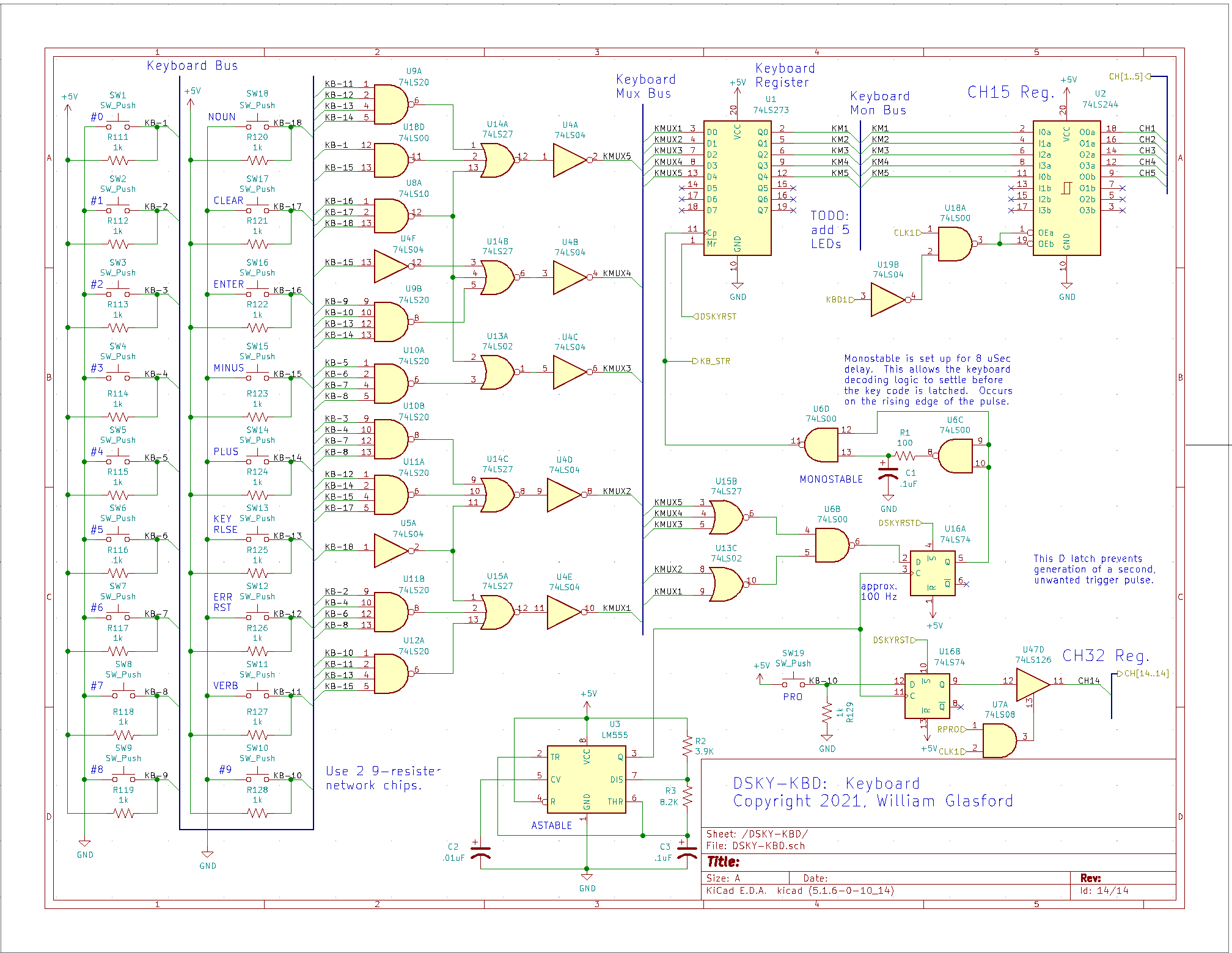
DSKY
07/06/2022 at 23:31 • 0 commentsThe DSKY is a separate physical piece of hardware with a simple interface consisting of the 15-bit channel bus and a handful of control signals. I built this as a stand-alone piece that started out as two boards and then grew to three boards. I have tried two different implementations and have finally settled on a third implementation. This has been slow going as during the pandemic I have been stymied with a shortage of certain chips. I first tried using only simple TTL chips and it got a bit too complex. I then discovered an LED driver chip and decided to go with those. I purchased three of these chips and discovered I needed a fourth and I have been waiting for 6 months for availability to complete this sub-system.
![]()
![]()
![]()
![]()
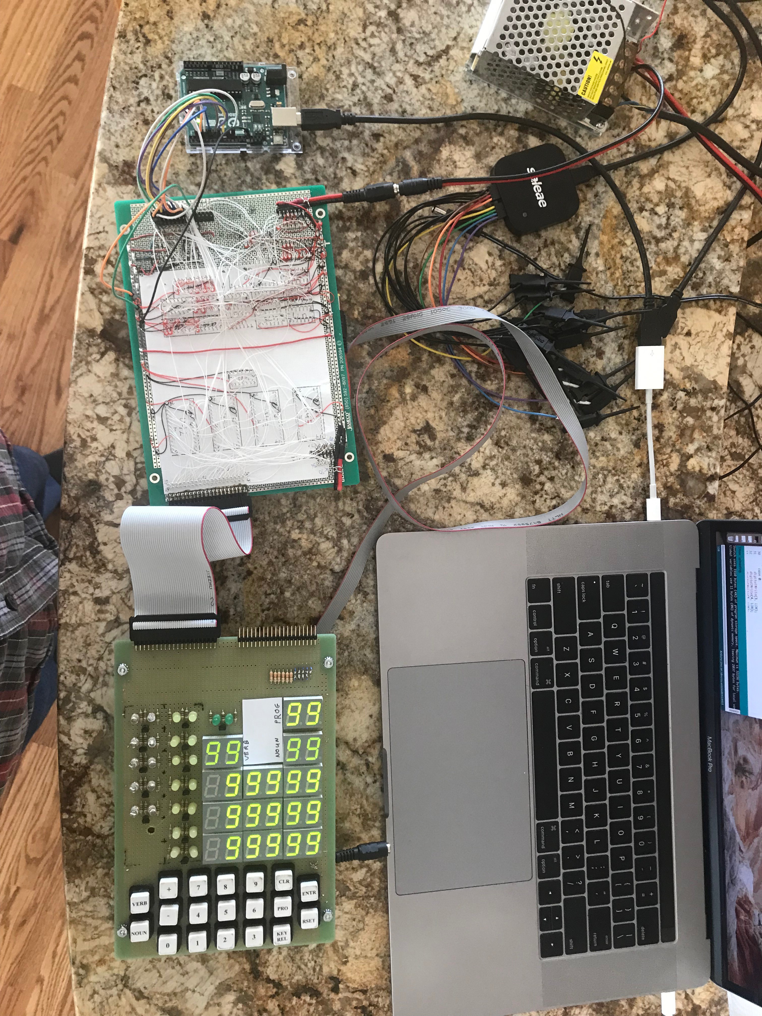
I test this sub-system with a Raspberry Pi driving the data lines. Here is picture of that setup.
![]()
As soon as I get the remaining chips I need I will complete this sub-system. In the mean time I made a paper model of the DSKY and that sent me down the path of building a better looking model of the DSKY. See my DSKY Model project for the progress on that DSKY. Both DSKYs are designed to connect to the AGC.
Here are some of the design notes that will help understand the schematics.
Keyboard: This module implements 19 switches. These switches are converted into a keyboard code using gate logic that is stored in the Channel 15 register. The keyboard codes, their meaning are defined in the following table.
Key A B C D E ID 1 0 0 0 0 1 1 2 0 0 0 1 0 2 3 0 0 0 1 1 3 4 0 0 1 0 0 4 5 0 0 1 0 1 5 6 0 0 1 1 0 6 7 0 0 1 1 1 7 8 0 1 0 0 0 8 9 0 1 0 0 1 9 0 1 0 0 0 0 0 Verb 1 0 0 0 1 a Reset 1 0 0 1 0 b Key Rel 1 1 0 0 1 c "+" 1 1 0 1 0 d "-" 1 1 0 1 1 e Enter 1 1 1 0 0 f Clear 1 1 1 1 0 g Noun 1 1 1 1 1 h The keys are pushbuttons that are normally high. A keypress presents a zero to the logic equations. Negative logic presents the easiest solution. All the lines of interest are normally 1. The logic for each of the five code bits is looking for a key to go low. The logic equations utilize 3 and 4 input NAND gates along with 2 and 3 input NOR gates. The results is NOTed. The equations are as follows.
A = (a * b * c * d) + (e * 0) + (f * g * h)
B = (8 * 9 * c * d) + e + (f * g * h)
C = (4 * 5 * 6 * 7) + (f * g * h)
D = (2 * 3 * 6 * 7) + (b * d * e * g) + h
E = (1 * 3 * 5 * 7) + (9 * a * c * e) + h
Notice that some of the portions of the equations are the same. For instance, A, B and C both have the (f * g * h) portion.
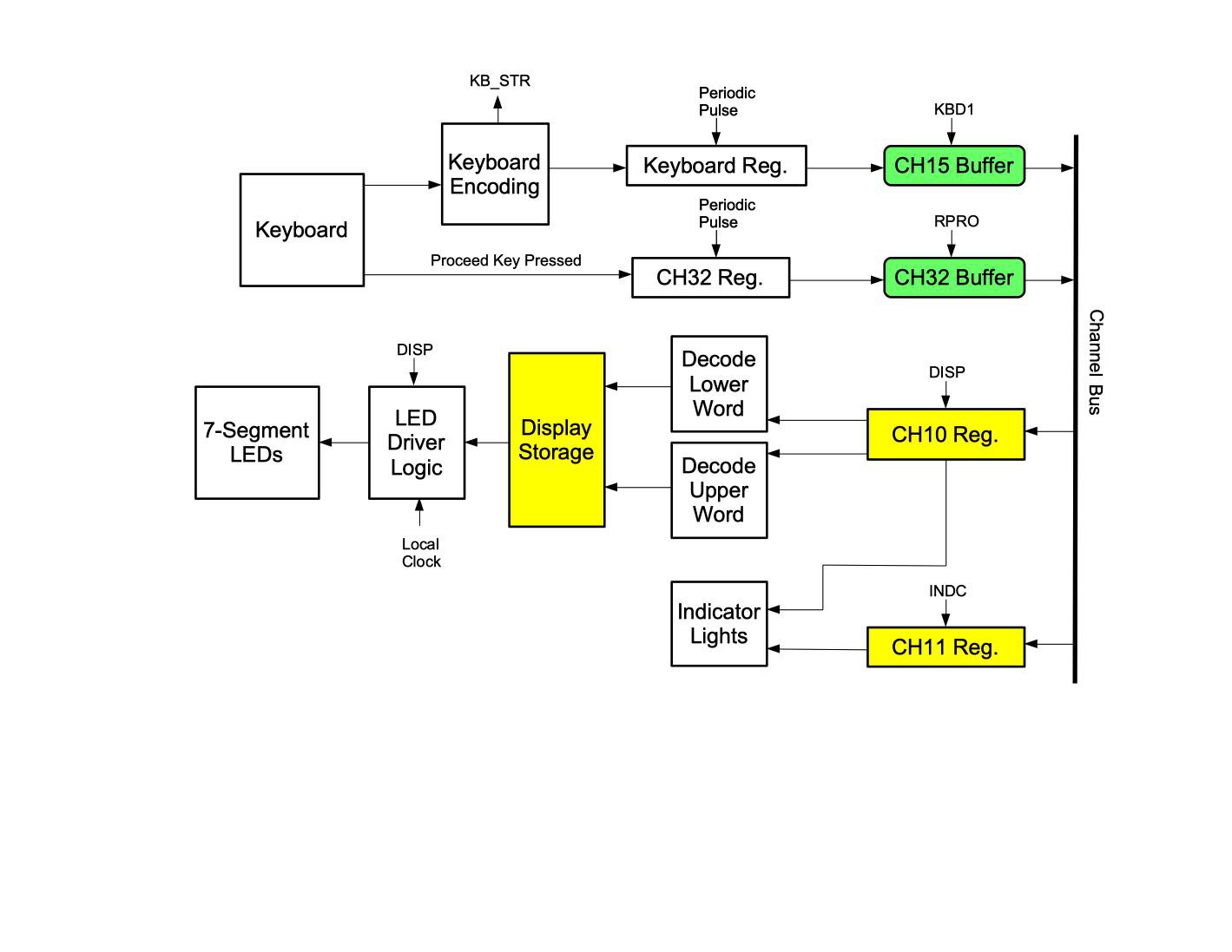
Display: The Display module implements the Channel 10 and 11 registers. Channel 10 is used to write data to the 7-segment LEDs two LEDs at a time. Channel 11 is used to light various indicators. Eight indicator are controlled using Channel 11. Another eight are controlled using Channel 10 with a specific relay word.
It should be noted that all the miscellaneous timing pulses using 555 chips are set up as astable multi-vibrators.
Most of the display logic decodes the Channel 10 value which is used to drive the 7-segment displays as pairs of numbers. Each output to this register drives two 7-segment numbers along with the plus/minus signs and a few other indicators. The format of the register is bits 1-5 hold a low digit value (DSPL), bits 6-10 hold a high digit value (DSPH), bit 11 indicates the plus/minus sign (DSPC) and bits 12-15 contain the relay word (RLYWD).
RRRRSHHHHHLLLLL
According to Ron's website, it is unclear how to blank the sign LEDs. There is one that says light the “+” sign and one that says light the “-” sign. Ron chose to display a blank if both values are zero. There is also the case where both may be set. I am not sure if this is avoided in code, but I have decided to handle this as a blank the sign case. The following table shows the possible states and the results.
(+) State (-) State Plus Minus 0 0 0 0 0 1 0 1 1 0 1 0 1 1 0 0 The relay words and the digits each one drives is listed below.
RLYWD # DSPC DSPH DSPL 1011 11 n/a MD1 MD2 1010 10 Flash VD1 VD2 1001 9 n/a ND1 ND2 1000 8 UPACT n/a R1D1 0111 7 +R1S R1D2 R1D3 0110 6 -R1S R1D4 R1D5 0101 5 +R2S R2D1 R2D2 0100 4 -R2S R2D3 R2D4 0011 3 n/a R2D5 R3D1 0010 2 +R3S R3D2 R3D3 0001 1 -R3S R3D4 R3D5 0000 0 (inactive state) 1100 12 Lights various indicator lights The 7-segment LEDs and their names are laid out as follows on the DSKY.
. . . . . . MD1 MD2 VD1 VD2 ND1 ND2 R1S R1D1 R1D2 R1D3 R1D4 R1D5 R2S R2D1 R2D2 R2D3 R2D4 R2D5 R3S R3D1 R3D2 R3D3 R3D4 R3D5 A decoder is required to convert from the 5-bit AGC code to a 4-bit hexadecimal number (BCD) that is understood by the BCD to 7-segment decode chips. The following table shows the two formats side-by-side.
Num AGC Hex 0 10101 0000 1 00011 0001 2 11001 0010 3 11011 0011 4 01111 0100 5 11110 0101 6 11100 0110 7 10011 0111 8 11101 1000 9 11111 1001 The two AGC values need to be decoded side by side, therefore the same logic is repeated twice. This logic uses four 3-8 bit decoder chips with values grouped based on the two high order bits. The outputs are individual lines that represent a numeric value in the table. These are then used as inputs to a pair of 8-3 bit encoder chips to get the required values in hex. The following table shows the table reordered based on the AGC bit values.
The two high order bits of the AGC value designate the chip number (1-4). The three low order bits are fed in as the value to decode. Each output line is given a designation based on the expected output hex value (L1-L15). These values are then fed into one of two encoder chips. One chip generates the values with the high order bit of zero and the other with a value of one. The logic of both chips is negative logic. The “active low” output line from the 74138 chips (Y0-Y7) are fed into the “active low” input lines of the 74148 chips (I0-I7). The resulting hex value is a combination of which chip is being used followed by the 3 digit value.
Num AGC 138 Chip# 138 Output Bus# 148 Chip# 148 Input Hex ' ' 00000 0 Y0 L15 1 I7 1111 1 00011 0 Y3 L1 0 I1 0001 4 01111 1 Y7 L4 0 I4 0100 7 10011 2 Y3 L7 0 I7 0111 0 10101 2 Y5 L0 0 I0 0000 2 11001 3 Y1 L2 0 I2 0010 3 11011 3 Y3 L3 0 I3 0011 6 11100 3 Y4 L6 0 I6 0110 8 11101 3 Y5 L8 1 I0 1000 5 11110 3 Y6 L5 0 I5 0101 9 11111 3 Y7 L9 1 I1 1001 Now that the data is decoded, each of the value pairs are stored in an 8-bit register. There are 11 registers to store the 21 values. To display the values, a timing pulse is generated that loops through the registers one at a time, feeding the values into 4 LED driver chips. I originally tried to squeeze the logic into three random access ICM7228 chips. The logic proved too complex. Upon reflection, I decided it would be much easier to use the natural address values of the relay words which would require a fourth chip. During the pandemic these chips fell into the category of “out of stock and no estimate of availability”. The only chips that were available were older, obsolete serial access ICM7218 chips. The downside of these serial chips is that the display digit values need to be stored external to the chip. This is because each time a value changes, all the values need to be re-written serially.
The digit enable numbers and their chip assignments are shown in the table below. Note that some addresses are not used, but are required given the serial nature of the chips. Also note that the values need to go into the chip in reverse. The DE column shows the reverse numbering, i.e. the numbering from the Display Control 154 chip.
RLYWD Digit Chip # Enable # DE 0 n/a 2 28 7 0 n/a 1 18 7 1 R3D5 2 27 6 1 R3D4 1 17 6 2 R3D3 2 26 5 2 R3D2 1 16 5 3 R3D1 2 25 4 3 R2D5 1 15 4 4 R2D4 2 24 3 4 R2D3 1 14 3 5 R2D2 2 23 2 5 R2D1 1 13 2 6 R1D5 2 22 1 6 R1D4 1 12 1 7 R1D3 2 21 0 7 R1D2 1 11 0 8 R1D1 4 48 15 8 n/a 3 38 15 9 Noun2 4 47 14 9 Noun1 3 37 14 10 Verb2 4 46 13 10 Verb1 3 36 13 11 Prog2 4 45 12 11 Prog1 3 35 12 12 n/a 4 44 11 12 n/a 3 34 11 13 n/a 4 43 10 13 n/a 3 33 10 14 n/a 4 42 9 14 n/a 3 32 9 15 n/a 4 41 8 15 n/a 3 31 8 These LED driver chips require 17 pulses to load them. The first write pulse sets the mode. Since this is the same value for each chip, one pulse will be applied to all four chips. The next 8 pulses set the first two chips data values and the following 8 pulses set the second two chips data values. This logic requires a 5-bit counter. Since there are many 4-bit counters, I chose to add a flip flop to be the fifth counter bit. Since not all the states are required and to take advantage of a single 4 to 16 bit decoder chip, I use the following states.
State Digit 11110 Start State 11111 Sent Mode 00000 First Data Value ... ... 01111 Last Data Value 10000 Stop Counting The OUTDAT pulse is as fast as 1 MHz which is much faster than the 2 Khz cycle timer to update the display and they are out of sync. To get them in sync one flip flop is used to capture the pulse. A second flip flop is then used to sync the signal. This is then used to start the counter and avoid a spurious write pulse. There are also two flip flops to represent the 5th bit of the counter. The first one captures the TC signal from the counter chip. The TC is set when all four bits are one. The next flip flop is set up as a toggle and toggles the next cycle, thereby changing to a one state when the counter goes to all zeros.
The DSKY consists of three boards. The front board is a solder board containing the astronaut facing keyboard, display and indicator lights. The middle board and back board are wire wrap boards. The middle board contains the four LED driver chips and the logic to drive the required data pulses. The back board is the majority of the logic.
-
Hardware Drawings
07/06/2022 at 23:15 • 0 commentsUp to this point I have been in my comfort zone, having spent my career as a software developer. Now it is off into the unknown of hardware development. The first thing I need is a good schematic drawing tool. After some research I decided to use KiCad. It is free, easy to use and seems to be what all the cool kids are using.
Note that all my schematics are out on my GitHub site at https://github.com/bglasford1 under the AGC Block II Computer project in the schematics directory. I chose to divide the project into five sub-systems; DSKY, Control, Processor, Memory and Display. The DSKY sub-system consists of the Keyboard, Display and Indicator modules. The Control sub-system contains the Clock, Scalar, Timing Pulse Generator, Sequence, and Control Pulse Matrix modules. The Processing sub-system contains the Arithmetic Logic Unit and Central Register modules. The Memory sub-system contains the Erasable Fixed Memory, Memory Buffer, Parity, Memory Address, Interrupts and Counters modules. The Display sub-system contains the Monitor module along with all the LEDs and switches from the Control, Processing and Memory sub-systems. The basis for splitting the modules up into sub-systems was to group like modules and to evenly divide them onto individual boards based on initial chip count.
I first had to create some data flow diagrams to visualize how this beast would be wired together and what pieces relate to other pieces. The data flow diagrams depict how the buses and registers interact with the control signals. The registers and logic blocks are rectangles and the bus drivers are round-tangles. The control signals that drive data into/out of registers and bus drivers are shown. The bus drivers and registers that are activated by the CLK1 pulse are colored green, the ones activated by the CLK2 pulse are colored yellow and the ones activated by the CLK3 pulse are colored cyan. This allows a quick visualization of the multi-stage data flow control during a single timing pulse.
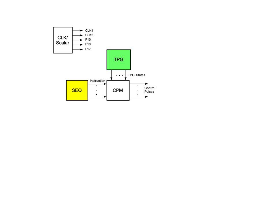
The following data flow diagram shows the overview of the control sub-system which includes the Timing Pulse Generation, Sub-sequence and Control Pulse Matrix modules as well as the Clock and Scalar modules. The Clock and Scalar modules simply create various clock pulses. The Timing Pulse Generation module uses a slightly delayed CLK1 pulse to transition between 12 timing pulse states as well as a few other debug states. The Sub-sequence module maintains the parts that make up the next instruction, to include the stage, sequence and branch values. These along with the timing pulse state are fed into the Control Pulse Matrix module which uses these values to look up the control signals from the control pulse matrix EPROMs. These control signals along with other internally generated signals cause the other modules to perform actions. These control pulses are generated during the rising edge of the CLK1 pulse. The other modules act on the read control signals immediately and delay the write signals until the start of the CLK2 pulse.
![]()
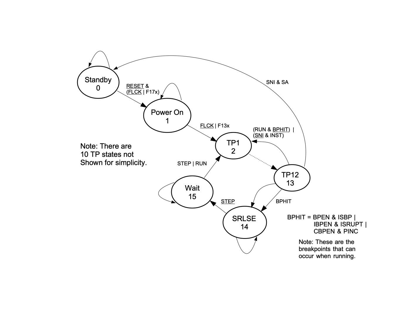
The Timing Pulse Generator is a state machine that controls the states a sub-sequence goes through. This includes the start up states and states that allow one to debug the system. Many of the states loop back on themselves, waiting for a specific input to transition them to the next state. Once in the TP1 state, the state machine transitions through to TP12 each clock pulse. The intermediate states are not shown for clarity. At TP12 the state can transition to a wait state if a breakpoint is set or to standby if the standby switch is set or loop back to TP1 if free running. Notice that if none of these states is set it simply transitions to the wait state. The wait state is preceded by the Switch Release state. Under each state name is a number that is the internal numeric depiction of the state.
![]()
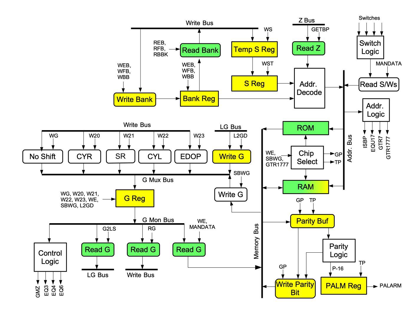
The following data flow diagram shows the memory logic and how various memory modules interact and how they are controlled by control pulses. The data written to certain values (020, 021, 022 & 023) go through shift registers before being written to the G register. All data moving onto and out of memory goes through the G register.
![]()
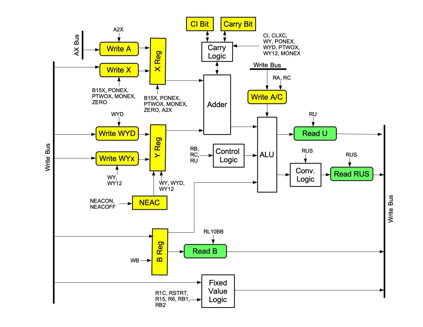
The following data flow diagram shows how the various modules that make up the Arithmetic Logic Unit interact and how the control pulses manage the logic. The X and Y registers are used as inputs to the adder that adds the two values. The results of the adder and the B register can be manipulated in various ways using a set of ALU chips. The output is considered the U register.
![]()
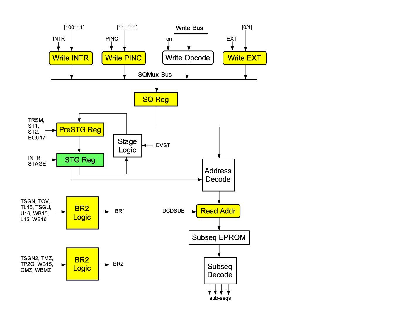
The following data flow diagram shows how the pieces of the Sub-sequence module interact and how the control pulses manage the logic. The Sequence register is the opcode of the next instruction unless a PINC sub-sequence or an interrupt occur. This value along with the Stage register are used to determine the next instruction sub-sequence to run. The branch values are used by the Control Pulse Matrix module to determine the next control signals to assert.
![]()
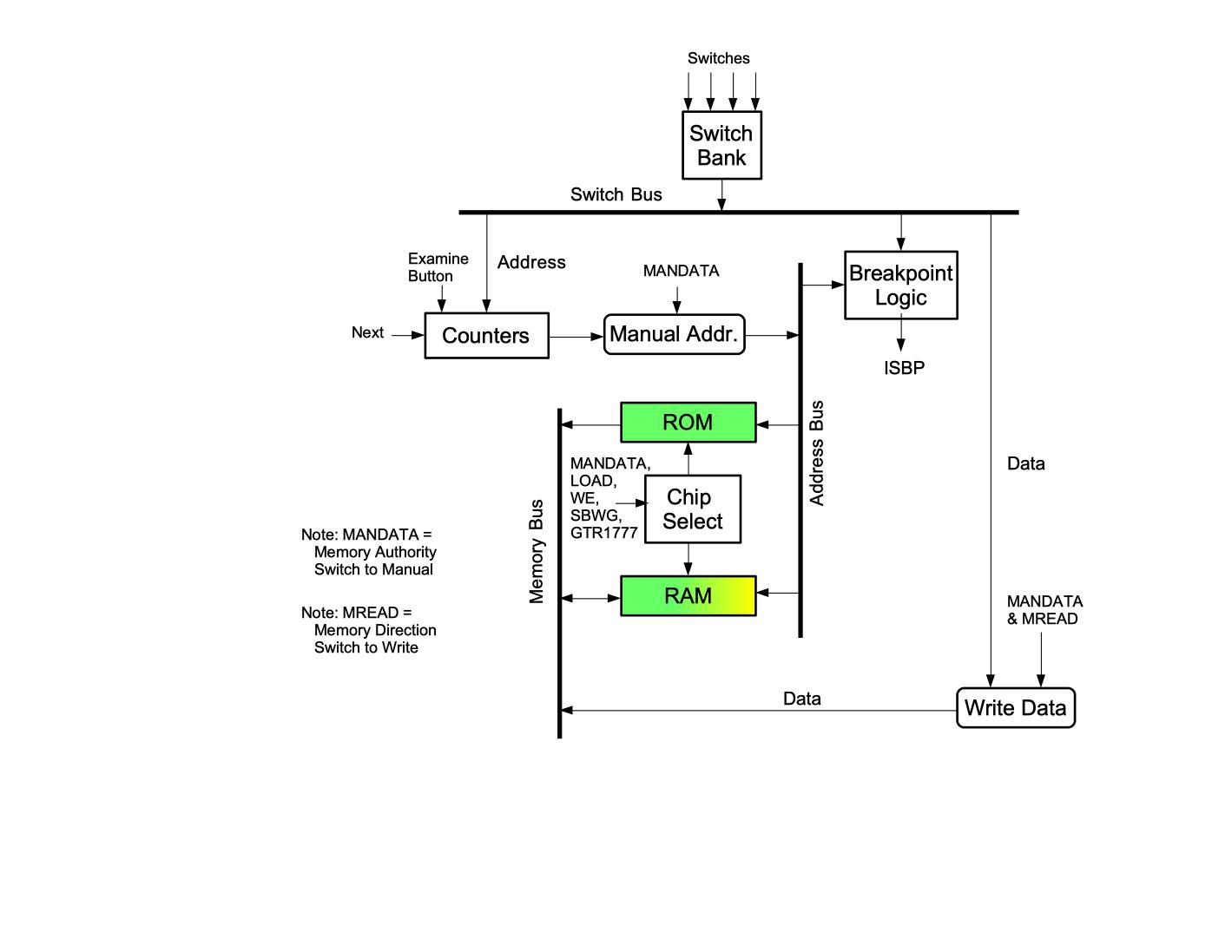
The following data flow diagram shows how the manual switches are used to read data from a given memory location, write data directly the memory bus and to check to see if a breakpoint address has been reached.
![]()
The following data flow diagram shows the counter logic. When appropriate, a runPINC control pulse is generated. This signal causes the PINC sub-sequence to run which increments the actual counter. Counters 1, 3 & 4 are incremented every 10 milliseconds when the F10X control pulse is asserted. Counter 2 is incremented when counter 1 overflows. The counter address is generated when the RSCT control pulse is asserted. This address is the address of the counter to increment.
![]()
The following data flow diagram shows the interrupt logic. There are three interrupts that can occur; RUPT3, RUPT4 and RUPT5 (keyboard data). The waiting interrupts are saved in the RPCell. When a RRPA control pulse is asserted, the current interrupt address is generated. This is the address of the jump table within the code. Interrupts can be inhibited.
![]()
The following data flow diagram shows how the DSKY is used to read data from the keyboard and write data to the 7-segment LEDs and the indicator lights.
![]()
I won't show pictures of each of the pages of schematics. There are over 100 pages. If you are interested, load up KiCad and give it a try. Currently the DSKY, DISP and MEM sub-systems are out there. I have sketched out the CTL and PROC sub-systems but have not yet published them. Here is one schematic page, the Keyboard.
![]()
-
Simulator
07/06/2022 at 22:44 • 0 commentsWhat sent me down this path was when I was looking for an historically significantly computer to build. I found John Plutorak's implementation of the AGC Block I computer. This was what I was looking for. I decided to push the boundary by focusing on the Block II version as that is the version that landed men on the moon. John built a hardware based simulator, but he wrote it in C and I much prefer Java.
I built a simulator that runs Block II code and provides a nice GUI interface to execute the simulation. The input files consist of the following S-Record files; the CPM files, the machine code file and a sub-sequence file.
Here is a screen capture of the simulator GUI. Notice that there are sections that simulates the DSKY, namely the Keyboard, Indicators and Display. The Control section is used to control the simulator. The help menu has an explanation of how to control the simulation. You can step through individual instructions, through each sub-sequence or even step through the timing pulses. After I got a few instructions working I realized I needed to set a breakpoint and let the simulator free run to that point. You can also break on a specific interrupt or counter increment. There are Sim States that give you insight into the state of the running simulation. The remainder of the sections are the actual registers and key memory locations within the computer. As instructions are executed you can see how each register is affected. This screen is going to translate into a whole lot of LEDs.
![]()
As before, all the source code and files required are out on my GitHub site.
-
Assembler
07/06/2022 at 22:30 • 0 commentsRon provided an assembler and all the available assembly listings. People went to museums and hand entered the assembly code and verified it by assembling the code and running it through Ron's simulator. That was a HUGE effort and HUGE thanks to everyone involved in that effort.
All I did was extend the assembler by adding an option to output the machine code in a Motorola S-record format. I use this output file as an input into my version of the simulator and as input into my ROM burner to burn the code into an EPROM for the hardware I am developing.
My modifications to Ron's assembler can be found on my GitHub site at https://github.com/bglasford1 Under the AGCBlockIIComputer project there is a YUL directory that contains my modifications. The original assembler was named YUL because they had a Christmas deadline. You can recreate the assembler I am using by first downloading Ron's yaYUL code and then adding my modifications to it.
Apollo Guidance Computer
A running hardware implementation of the AGC, block II using TTL chips.