Guido
Guido-
The ADC board analog input
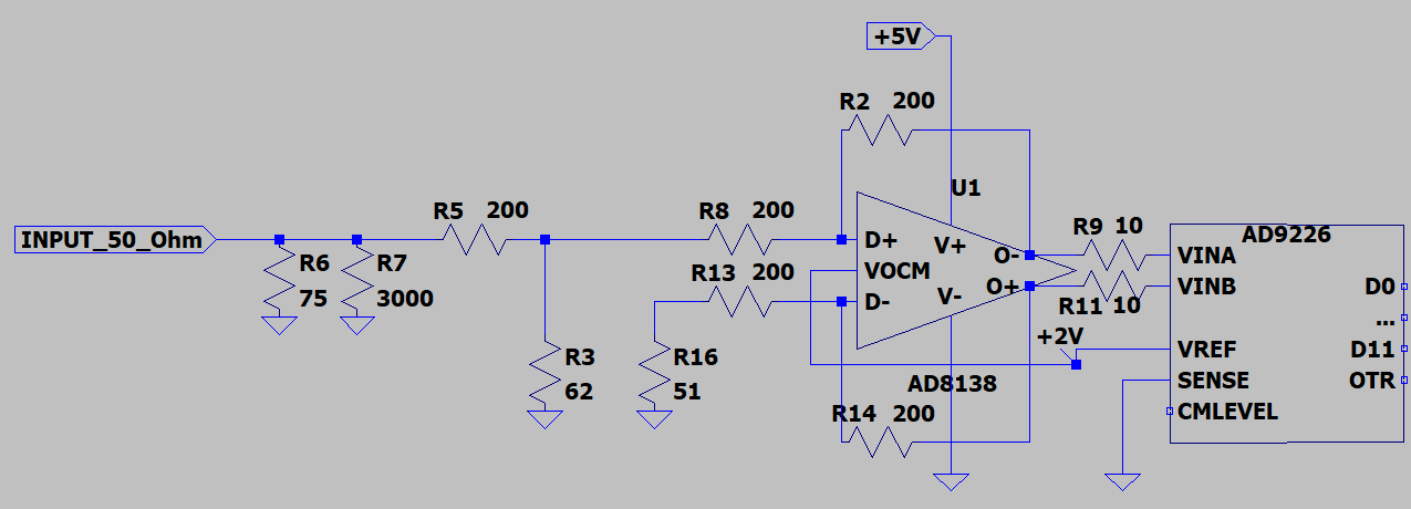
11/09/2022 at 19:51 • 0 commentsThe second lesson I learned was about the unbalanced -> balanced amplifier AD8138 feeding the balanced AD9226 input. Its analog input schematic for the board I used is something like this:
AD9226 12-BIT 65 SMPS BOARD - original schematic
![]()
Therefore the overall amplification between VINA-VINB and INPUT_50_Ohm is approximatively:
200//62
-------------------- x (200/200 + 1) = 0,38 i.e. -8,4 dB
200 + 200//62
Well, connecting my End Fed Long Wire Antenna to the Input_50_Ohm I realised that the AD9226 samples (12 bits) were around 0x820 and 0x07E. So I decided to amplify a bit :)
-
Connect the ADC
11/07/2022 at 22:37 • 0 commentsFinally I connected the ADC and a 1 MHz external sinusoid to its input (1 Vpp).
After some struggling and debugging I understood that the AD9226 board wasn't coding "two's complement" but as an unsigned integer i.e.
1 V -> FFFF FFFF FFFF
0 V -> 7FFF FFFF FFFF
-1 V -> 0000 0000 0000
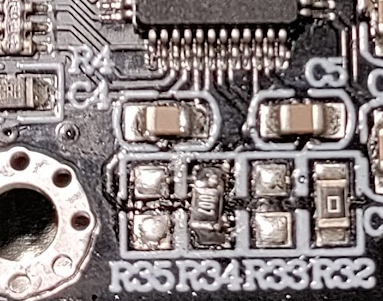
Later I noticed (reading the AD9226 datasheet ... I didn't do it before) that AD9226 features:
Straight Binary or Two’s Complement Output Data
In fact the ADD9226 board has R35 and R35 to set Straight Binary (Factory Default) or Two's Complement.
As I preferred Two's Complement, I changed R34 and R35 in this way.
•R35: not connected
• R34: 10KOhm
![]()
-
Added an internal (FPGA) RF Generator
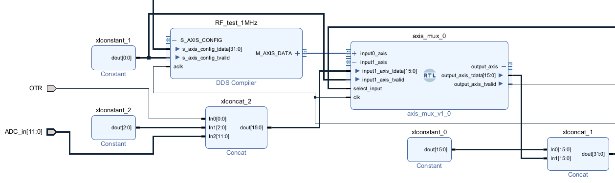
11/07/2022 at 22:07 • 0 commentsJust to go step by step, before connecting the external ADC, I added an internal RF generator (1 - 30 MHz).
The DDS compiler block with name "RF_test_1MHz" can generate a sinusoid encoded on 12 bits (two's complement).
Using an AXIS MUX "axis_mux_0" you can select (see the line select_input) the real ADC_in or the RF test generator.
Please note that the result is encoded on 32 bits:
- the 1st an 2nd byte contain the 12 bits data sample + 1 bit for "Over The Range"
- the 3rd and 4th byte are 0
In this way I'm ready to handle the IQ samples (16 + 16 bits).
-
Set a HW SW IDE to develop easily
09/18/2022 at 19:48 • 0 commentsAfter many different attempts, I setup an HW SW IDE to easily program the EBAZ4205.
Not to overwhelm this project, I created a new dedicated Hackaday project EBAZ4205 HW SW IDE
-
Built the very first assembly for a few experiments
08/29/2022 at 06:20 • 0 commentsAs you can see in the section "first assembly", I boxed the AD9226 ADC and connected it to the EBAZ4205. Using Xilinx Vivado now I would like to test the single components: 65MHz clock generator output, Analog to Digital capabilites, Digital Down Conversion and so on.
-
Received the EBAZ4205, that works as expected!
07/30/2022 at 13:33 • 0 commentsJuly 27th, 2022
I received the EBAZ4205 board from China.
July 29th, 2022
Tested the PS (Programmable System i.e. the CPU) of the board successfully. -
July 2nd, 2022 - Started working
07/29/2022 at 05:53 • 0 comments
Waiting for the boards I ordered from China, I started examining the schematics. See the Details section.
32MHz spectrum + SDR + FT8 in an FPGA
A 0 - 32MHz FPGA based Software Defined Radio (AM SSB FT8) by ready modules->cheap and easy Last add: Aug 14th SW update to include GFSK