Guido
Guido-
AD9851 IP - second attempt.
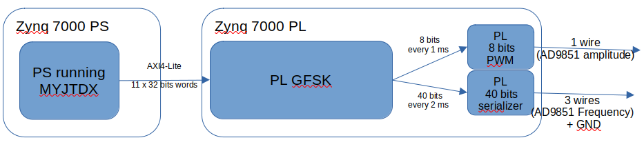
09/11/2023 at 08:53 • 0 commentsA FIFO component receives via AXI4-Lite the 79 symbols (each symbol is 3 bits each) composing the FT8 message. In this way the Linux software (MYJTDX) and the Cortex A9 CPU have plenty of time to send these 21 x 32 bits every 15 seconds. Besides, the carrier frequency (e.g. 7075500 Hz) must be sent to the AD9851.
![]()
Therefore the message from PS to PL could be composed by the following 11 x 32 bits words.
MSB LSB
- R0 : Phase shift for the carrier frequency (when symbol value=0): 32 bits
- R1 : Symbol 8 (4 bits) Symbol 7 (4 bits) ... Symbol 1 (4 bits)
- ...
- R10 : Symbol 73 (4 bits) ..... Symbol 79 (4 bits) Symbol 73(4 bits)
- R11 : 0 ... ... 0 PWM max value (8 bits) TODO
NOTE Please note that an FT8 symbol (0...7) could be encoded with 3 bits but for AXI4-Lite convenience (8 bits alignment) I decided to encode a symbol in 4 bits leaving the MSB at 0.
TODO: PWM Maximum Value
Lately I added the R11 register where I program the maximum DC value that the PWM can reach.
E.g. If I set PWM max value to 153, PWM can go from 0 Volts (duty cycle 0%) to 3.3 x 153 / 255 = 1,98 Volts.
This parameter, programmable by myjtdx (PS side) allows to be sure that when the PWM DC level is:
- at its maximum value, the AD9851 outputs nothing
- near the maximum value, the AD9851 outputs a minimal signal.
As I already built the AD9851 PWM and AD9851 serializer, it's now time to design the GFSK IP.
-
Vivado AD9851 first attempt
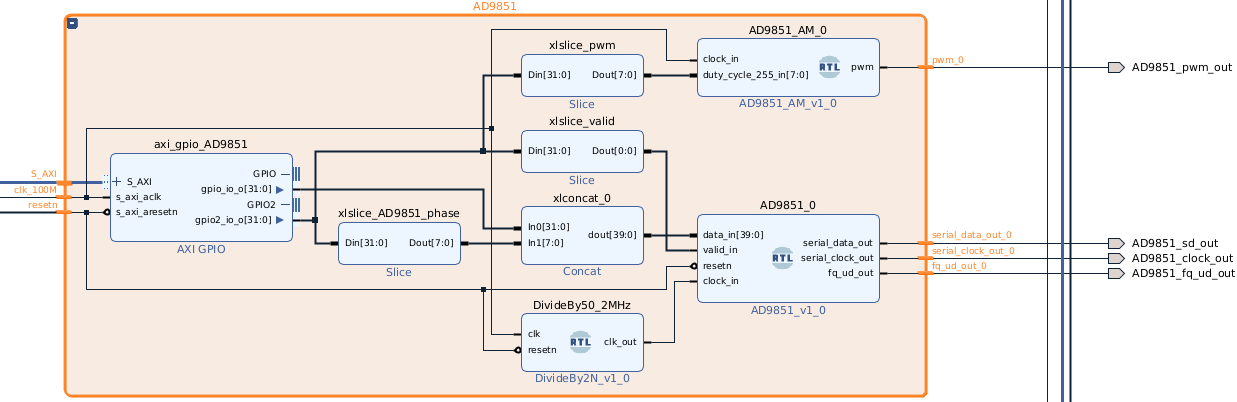
09/11/2023 at 08:31 • 0 commentsThis solution would work (with a faster CPU) but the Zynq7010 Cortex A9 CPU isn't able to send a new word (32 bits phase shift) every 1 or 2 milliseconds with enough timing precision. I'm now trrying to implement an all PL solution. See next log.
![]()
The AD9851_0 VHDL IP is controlled by a GPIO IP (axi_gpio_AD9851) where the two 32 bits output ports act as:
- Port 0: 32 bits DDS phase increment to the AD9851 according to the formula:
Out frequency = phase_increment * 180 MHz / 2^32
- Port 1:
- bits 31 ... 17 : not used
- bit 16 : valid_in signal to the AD9851_0 IP
- bits 15 ... 8 : pwm duty cycle (0 - 255) to AM modulate the output
- bits 7 ... 3 : output phase (always 0)
- bits 2 : power down (0=power out 1=power down)
- bit 1 : always 0
- bit 0 : AD9851 6x (ask the AD9851 to multiply by 6 the 30MHz reference to obtain a 180 MHz clock reference)
-
FT8 message software implementation
09/02/2023 at 11:09 • 0 commentsJTDX and WSJT-X prebuild the FT8 message audio samples (at 48KHz) and send them altogether to the PC audio card whose output modulates the SSB (USB) transmitter. In this case, the task to precisely send out the 81 FT8 symbols is in charge of the audio card.
Of course I cannot follow this method because, as I explained in the log FT8 QSO's, I chose to use an external sinusoidal DDS synthesizer that I need to modulate in amplitude (for the 1st an 81st symbols only) and frequency for the whole 81 symbols. Therefore I need to change amplitude (8 bits encoded) and frequency (32 bits encoded) at a proper speed.
For the amplitude
The first symbol has a 20 milliseconds ramp-up (shaped as a raised cosine) and a remaining 140 milliseconds at constant amplitude
The last (81st symbol) has a 140 milliseconds duration at constant ampltude and a remaining 20 milliseconds ramp-down (shaped as a raised cosine)
I suppose that I can approximate the raised cosine ramp-up o ramp-down with 20 samples (1 sample every millisecond). E.g. 0 0.01 0.02 0.03 0.05 0.07 0.10 0.15 0.20 0.40 0.60 0.80 0.85 0.90 0.93 0.95 0.97 0.98 0.99 1
For the Gaussian Frequency Shift Keying
The frequency change is every 160 milliseconds (1 symbol duration) but it is smoothed with a Gaussian function, to reduce band occupation. MYJTDX produces the frequency shift samples at 48KHz so that, for every 160 milliseconds symbol we have 7680 samples. The maximum shift (from value 0 to value 7) is 7 * 6,25 Hz=43,75 Hz and can happen in about 32 milliseconds (0.2 * 160 milliseconds)
-
Creating a Vivado IP to program the AD9851
08/16/2023 at 20:14 • 0 commentsAccording to the previous evaluations (see previous logs), I should build something like this:
![]()
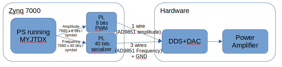
- PL 8 bits PWM to set amplitude (ramp up of 1st symbol and ramp down of 81st symbol)
- PL 40 bits serializer to set frequency
are two Vivado IPs receiving the 8 + 48 bits from a GPIO standard Vivado IP
-
How to use the frequency shift array pre calculated by JTDX
08/16/2023 at 19:52 • 0 commentsThe C code of JTDX is written to create the 81 samples (sampled at 48 KHz - S16LE) of the 8FSK message lasting 12,96 seconds. However, one of its intermediate products is the phase shift (dphi) of the 8FSK modulated signal, sampled at 48KHz.
For each FT8 transmission, dphi contains 81*48000*0,16=622.080 samples of the transmitted frequency, for a total last of 12,96 seconds.
-
FT8 protocol
08/11/2023 at 18:04 • 0 commentsTo build an FT8 modulator I need to resume the FT8 message format. All the details come from FT4_FT8
The 174 bits message
A single 174 bits TX message is composed by:
- 77 bits the message content
- 14 bits Cyclic Redundancy Code
- 83 bits Forward Error Correction
77 bits 14 bits 83 bits message CRC FEC The 81 symbols
- The 174 bits are grouped 3 by 3 obtaining 58 symbols
- Each symbol lasts 0,16 seconds
- The 58 symbols are interposed (beginning, middle and end) by 7 grey coded symbols to ease synchronization
- a single initial symbol (3) increases the amplitude with a ramp up to max amplitude
- a single final symbol (2) decreases the amplitude with a ramp down to 0
ramp up
1 sym
(*)grey code
preamble
7 symsFirst half
29 symsgrey code
7 middle symsSecond half 29 syms grey code
queue 7 symbolsramp down
1 sym3 3 1 4 0 6 5 2 S0....S28 3 1 4 0 6 5 2 S29.....S57 3 1 4 0 6 5 2 2 The total message lasts 160 milliseconds x 81 symbols = 12,96 seconds
8FSK modulation
Each symbol, which lasts 160 milliseconds, generates 1 of 8 frequencies shifted by 6,25 Hz i.e.
- sym: frequency shift
- 0 : 0 Hz
- 1 : 6,25 Hz
- 2 : 12,50 Hz
- 3 : 18,75 Hz
- 4 : 25 Hz
- 5 : 31,25 Hz
- 6 : 37,50 Hz
- 7 : 43,75 Hz
The frequency doesn't shift immediately between a symbol and the next, but it is smoothed with a Gaussian function (see Figure 2 in the article FT4_FT8).
-
FT8 QSO's
07/21/2023 at 07:52 • 0 commentsOverview
Now that the whole project works pretty well as a receiver, including FT8 decoding, it's time to transmit anything.
To understand the FT8 protocol, see FT4_FT8
MYJTDX software (forked from JTDX forked from WSJT-X) decodes well and it is ready to transmit and manage QSO's. Its way to transmit is to send an 8FSK modulated tone at 1500Hz out to the audio out card (to the PL of Zynq7000). This tone would SSB modulate an HF transmitter.
E.g. 8FSK 1500Hz modulates in USB a 7074000 Hz transmitter, obtaining a 7075500 Hz 8FSK modulated carrier.
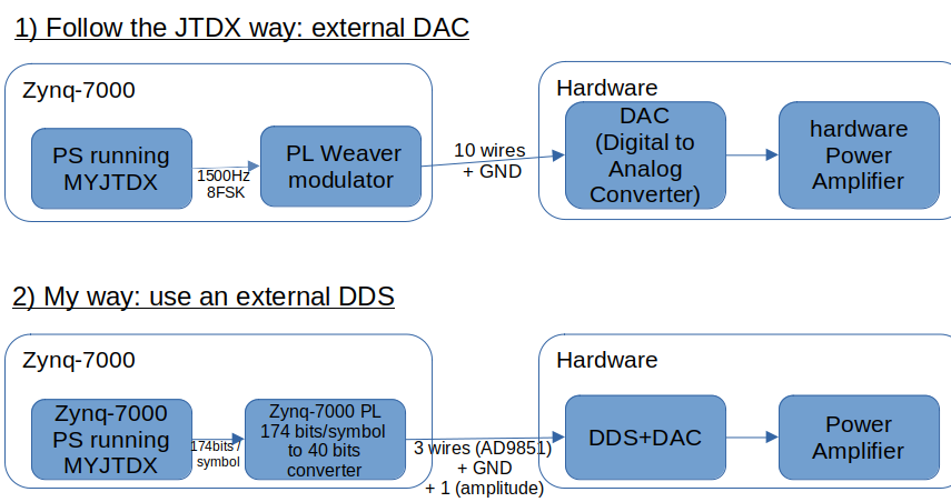
Now I see two options
1) Follow the JTDX way - external DAC, sending the 1500Hz 8FSK modulated tone to a USB Weaver modulator.
1500 Hz 8 FSK audio samples from PS to PL -> Digital Weaver USB modulator -> hardware DAC -> hardware HF amplifier -> Low Pass Filter -> Antenna
2) Use an external DDS, programming its output frequency to produce 8FSK and amplitude to generate the ramps (raised cosine initial amplitude increase and final amplitude decrease) of FT8.
174 bits encoded sequence from PS to PL -> external AD9851 DDS -> hardware HF amplifier -> Low Pass Filter -> Antenna
![]()
For AD9851 Amplitude Modulation see this
PRO'S and CON'S
Follow the JTDX way Use an external DDS Audio stream / Amount of data +++ The audio stream is produced by JTDX!
--- The audio stream must be transferred from PS to PL via DMA or similar
--- About 300 KBytes must be transferred from PS to PL every 15 secondsThere's no audio stream
+++ Only 174 bits (produced by JTDX) must be transferred from PS to PL every 15 secondsAvailable HW boards --- I didn't find any high speed DAC board +++ I found AD9851 (DDS + DAC) board for around 30 Euros or AD9850 for 20 Euros JTDX addition +++ None --- 3 bits FT8 symbol to 40 bits AD9851 programming word Vivado design --- Weaver modulator (2 x DDS compiler + 2 audio FIR filters + 4 multipliers) +++ 40 bits serial output with clock, word write and reset
--- PWM amplitude modulator for FT8 ramp up and down.Pins Usage --- Zynq7010 12 pins output (10 bits data + clock + strobe) +++ Zynq7010 4 pins (serial data, clock, word write, PWM amplitude) -
FT8 decoding
05/08/2023 at 07:32 • 0 commentsIt's now time to decode some radio ham digital modes, starting from FT8, which I'm very fond of!
The idea is to transfer the PCM audio stream from the PL to the PS, where a "standard" linux audio driver lets consume the stream using the FT8 software WSJT-X. See Overview block diagram.
Regarding the WSJT-X specific implementation on PetaLinux, I modified JTDX adapting it to the different software environment (without a windows manager) obtaining myjtdx
The Linux Audio Driver is described here Xilinx ALSA audio I2S driver
A Vivado project with an I2S Receiver and Transmitter, DMA and Linux Device Driver is very well described here:
In part 1 and 2 of Audio Linux Device Driver for (*) Zedboard - hardware implementation you can read the Vivado hardware implementation, while In part 3 you can read the PetaLinux building.
(*) Zedboard is an AVNET board based on Xilinx Zynq-7000
-
Keyboard and Mouse control
01/16/2023 at 21:21 • 0 commentsAfter obtaining an HDMI video out from the EBAZ4205 board and being able to use it from Linux by /dev/fb0, now I need to interact with Linux and the C / Python app (showing the spectrum, tuning and so on) with standard input devices keyboard and mouse.
For this need, I examined two options:
- USB
- PS/2
USB
Unfortunately EBAZ4205 has no USB interface, but I found the way to implement it using a cheap external module USB3300
I'm now looking forward to arriving it from China.
PS/2
- It's a bit obsolete but it is very promising because it doesn't need any hardware addition.
- I found an AXI PS2 IP controller from DIGILENT: AXI PS/2 1.0 IP Core User Guide from DIGILENT,. I tried to use it but I didn't succeed!
- So I decided to use some VHDL code I found here PS/2 Mouse Interface (VHDL). Unfortunately this VHDL code manage the two buttons PS/2 mouse only and not the middle button and the wheel (so called IntelliMouse), so I had to integrate the VHDL code.
- Then I also found a linux device driver xilinx_ps2.c with a similar memory mapped interface that I hope to be able to adapt.
You can follow the full Hackaday project EBAZ4205 PS/2 Mouse
-
Video Out
01/04/2023 at 09:19 • 0 commentsAs I explained before, I would like to embed the User Interface App into the PS side of Zynq.
The App, actually written in Python (Matplotlib + pyQTgraph), allows to see the spectrum, the waterfall and to tune radio stations.
For this reason the EBAZ4205 should have implemented with any kind of video out.
I examined a few options.
- VNC server / X11 forwarding
- Not difficult to do in SW
- No need to change hardware
- It needs an external PC
- VGA
- It needs a simple resistive external ladder
- a bit old fashioned
- it's analogic
- It needs an external VGA display or a VGA/HDMI external adapter
- HDMI with HW converter
- It uses an external device (ADV7511 or similar) to convert the Zynq parallel output to the HDMI differential digital signals to handle the highest resolutions
- It's digital
- you can use any HDMI display / TV
- HDMI without HW converter
- It doesn't use any external device, the Zynq pins are directly connected to the HDMI port
- For the HW implementation see Digilent ZYBO schematic at page 5 and Digilent ZYBO Reference at page 21
- For a SW test see Digilent HDMI demo having also the HDMI input side that is useless to me or Video Series 23: Generate a video output on Pynq-Z2 HDMI out which outputs a test pattern to the HDMI out
- It's digital
- you can use any HDMI display / TV
- VNC server / X11 forwarding
32MHz spectrum + SDR + FT8 in an FPGA
A 0 - 32MHz FPGA based Software Defined Radio (AM SSB FT8) by ready modules->cheap and easy Last add: Aug 14th SW update to include GFSK