-
Revisiting plasma etching
08/19/2024 at 20:13 • 0 commentsI didn't know how to control plasma, until I started to work with lasers. Two things I've learned first the white residue means it was too hot. Second, most Important, instead of power fan. I should use air pump just like laser does. With laser's air pump the air concentrated in very small tube, this way we may insure air/plasma is not too hot.
-
Cleaning residue
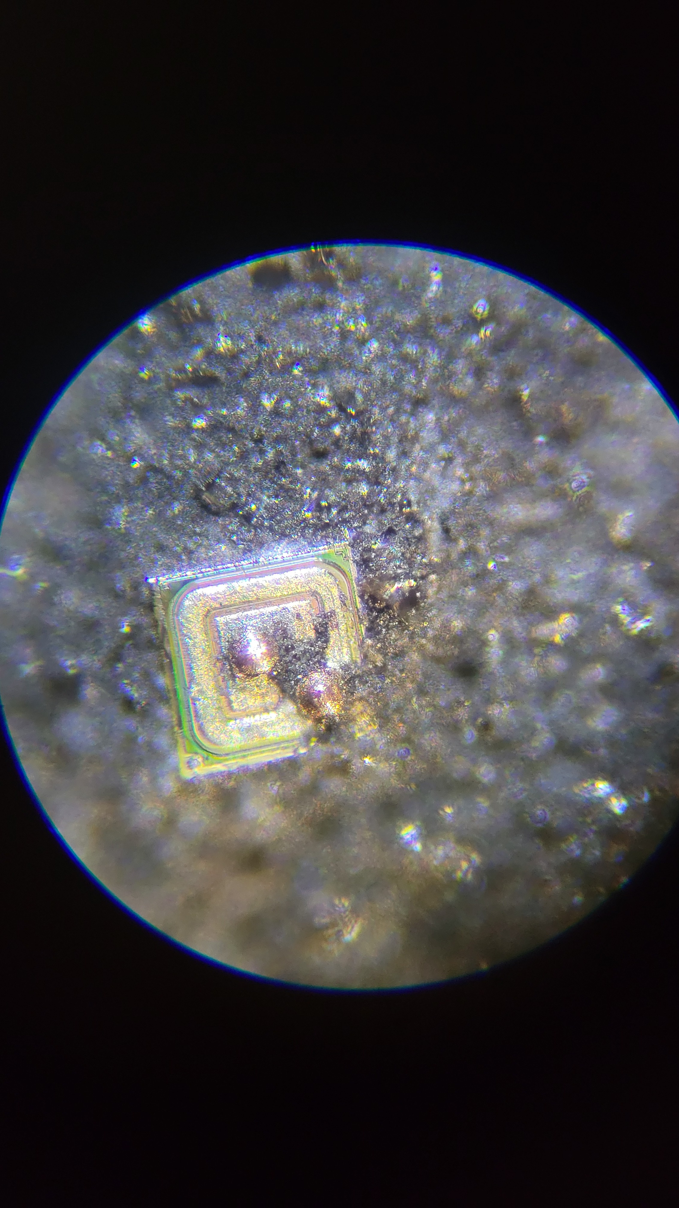
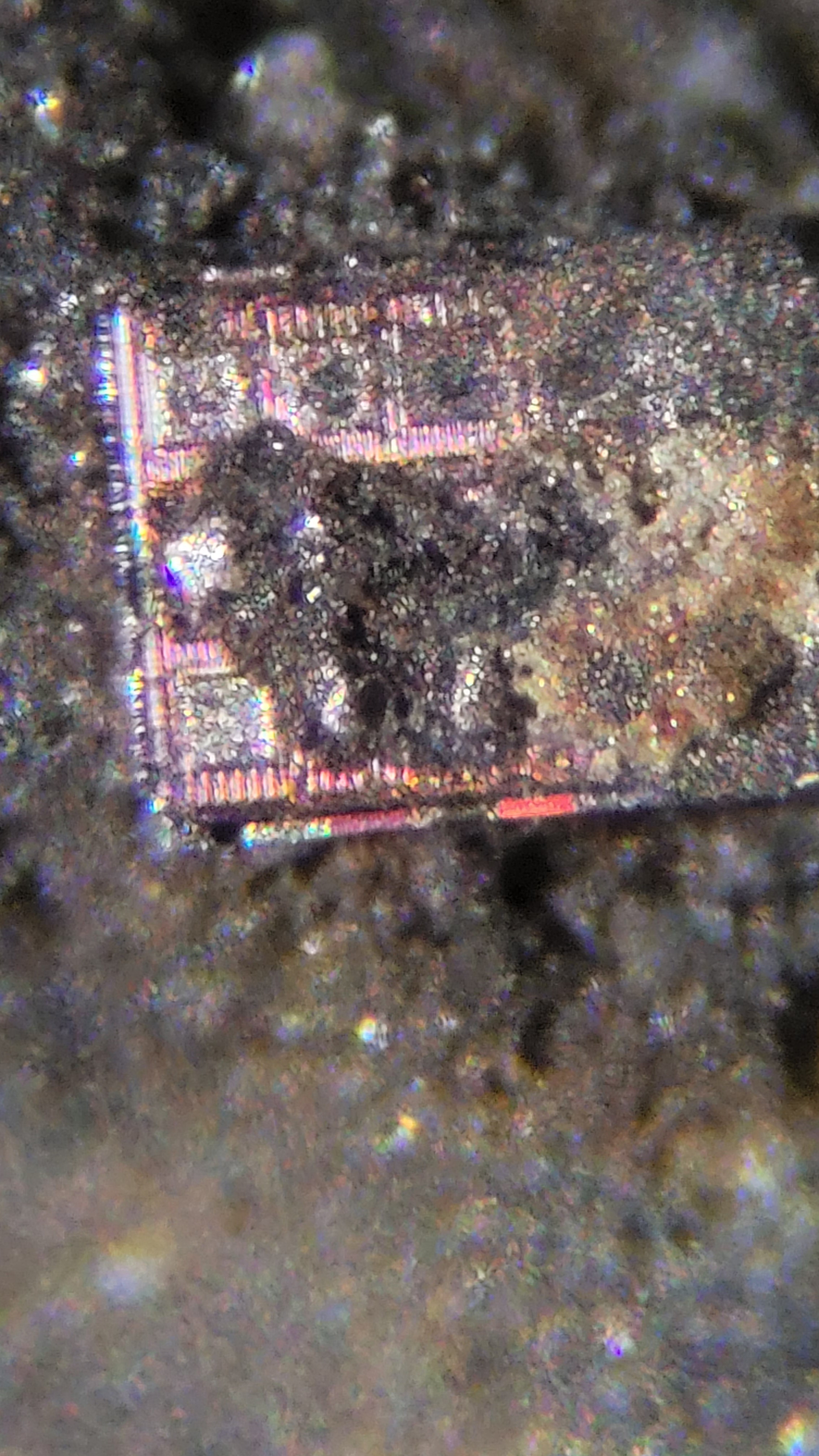
01/10/2024 at 18:27 • 0 commentsOne of the problems of hot gun decapsulation is that always there is some kind of residue left. This obscure the image. For example:
![]()
You can see some gray material between two bonding wires (or should I say what left from them)
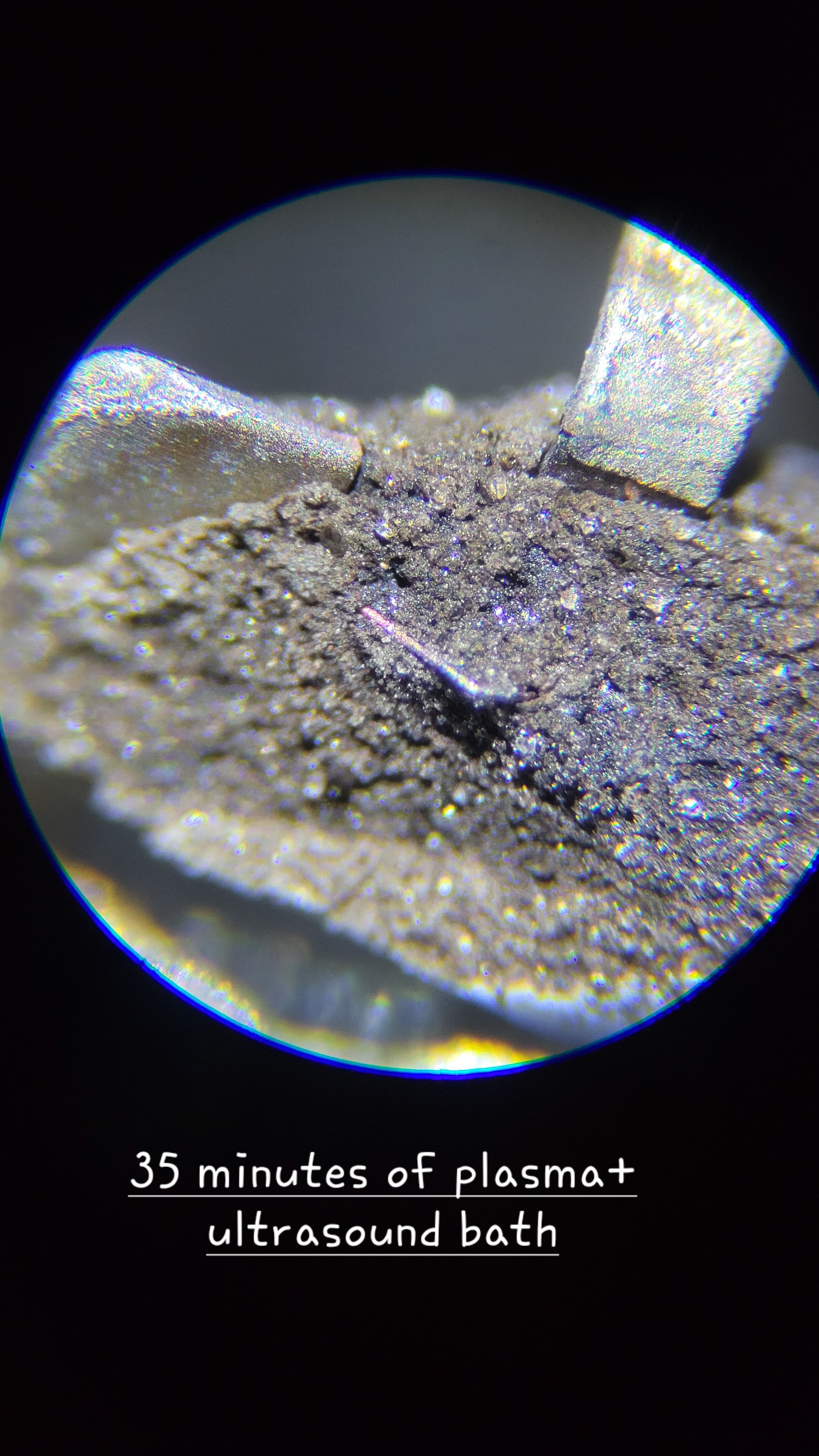
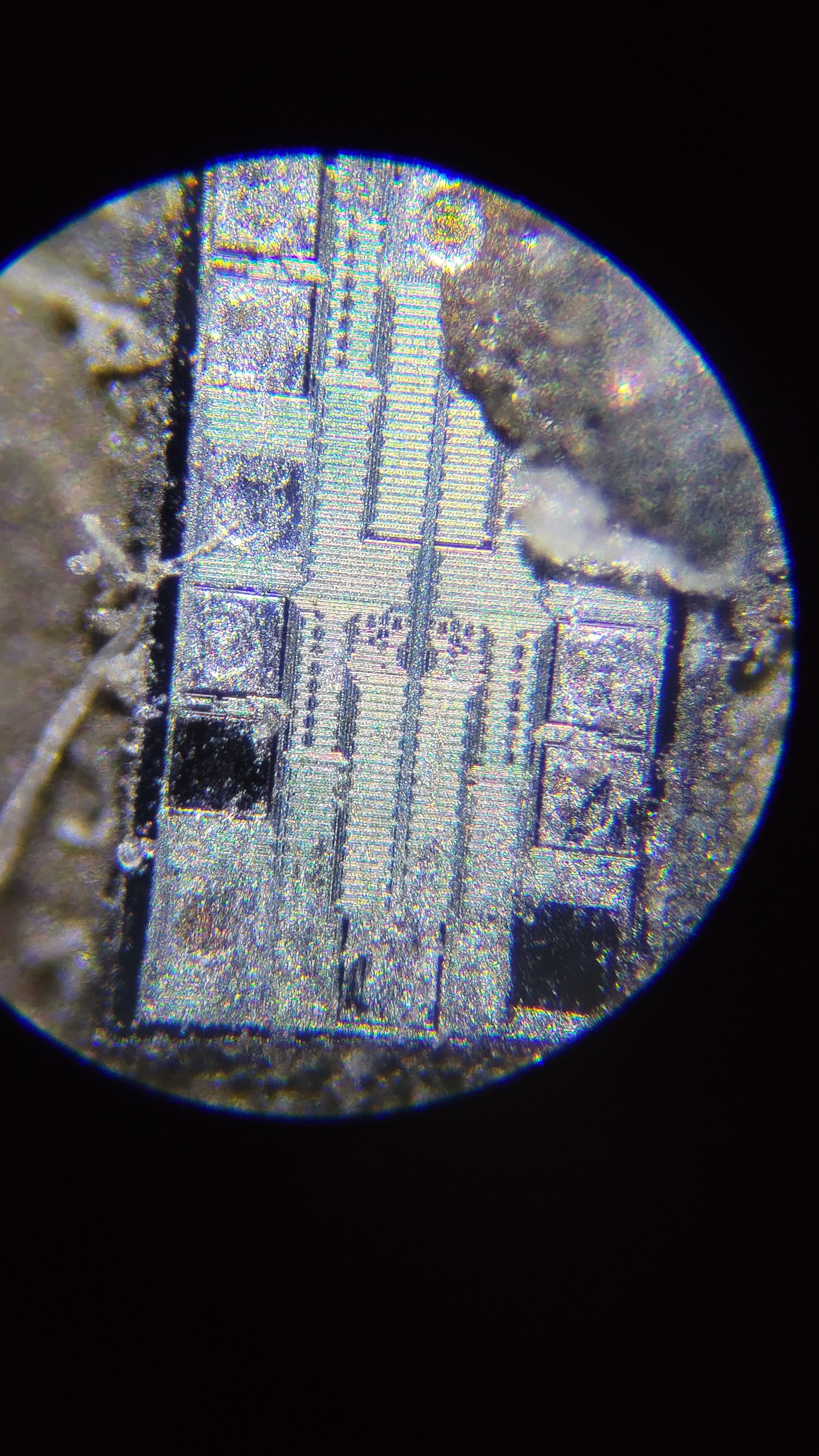
Now let's clean it up with some plasma and ultrasound bath. Now we get
![]()
Now it looks like the gray material is gone!
-
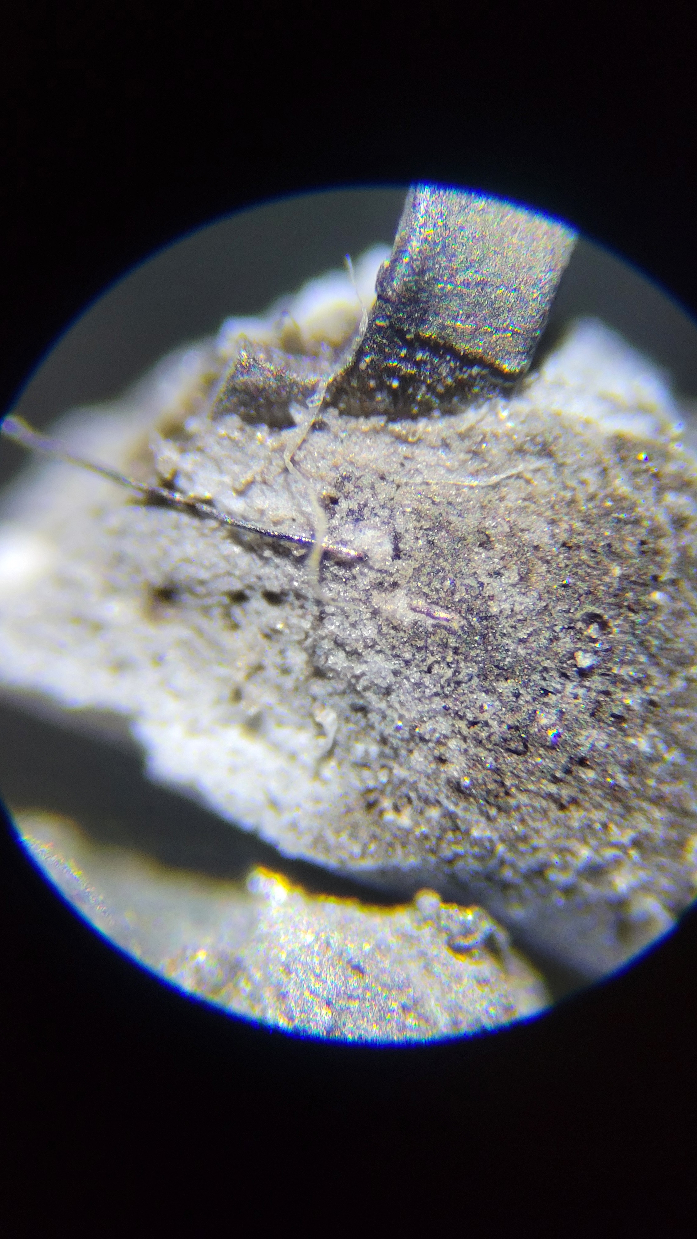
Bonding wires can survive plasma
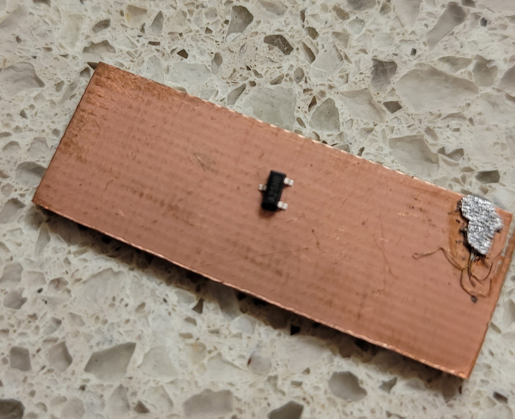
01/03/2024 at 07:09 • 0 commentsI thought I should start from the point I know it's working. So I used a thick copper wire to connect my SMD transistor and manually tried to decap it. I started etching and after a while I got my first SMD decaped transistor.
![]()
It's looks great isn't it?
But what about bonding wires? Can we save them?
The answer is yes, so it appears at least. Second transistor I was ready and with a lot of patience I made etching with bonding wires present.
![]()
After few hours af gentle decapsulation I got those two binding wires intact.
Clumsy me, one wrong move and one of the bonding wires turned to micro scrambled egg.
I don't give up yet ... I have a better idea... Stay tuned ...
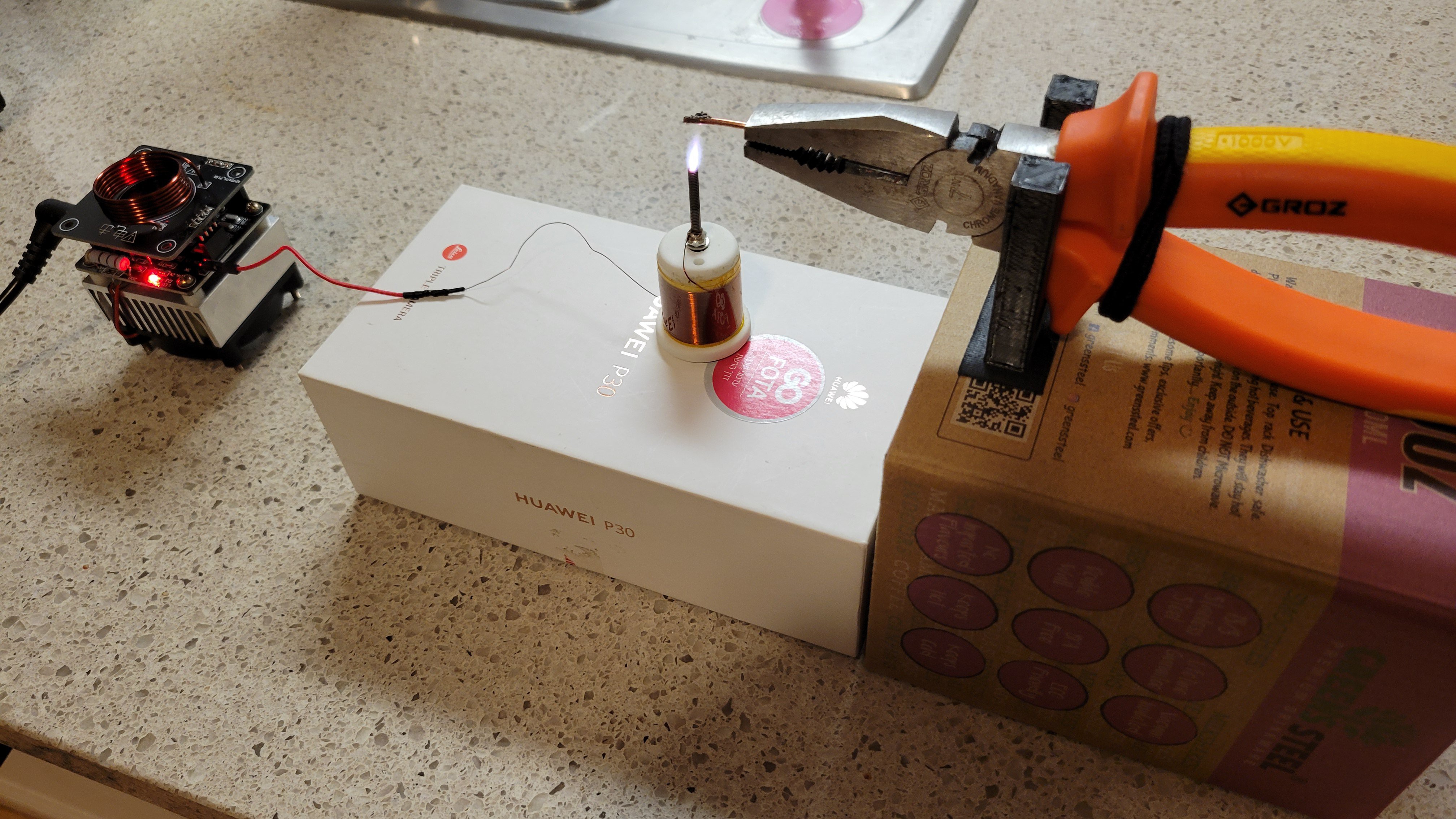
Instead of holding pliers I made this
![]()
Just a simple pliers holder. Now we can set plasma flame to right position. We got:
![]()
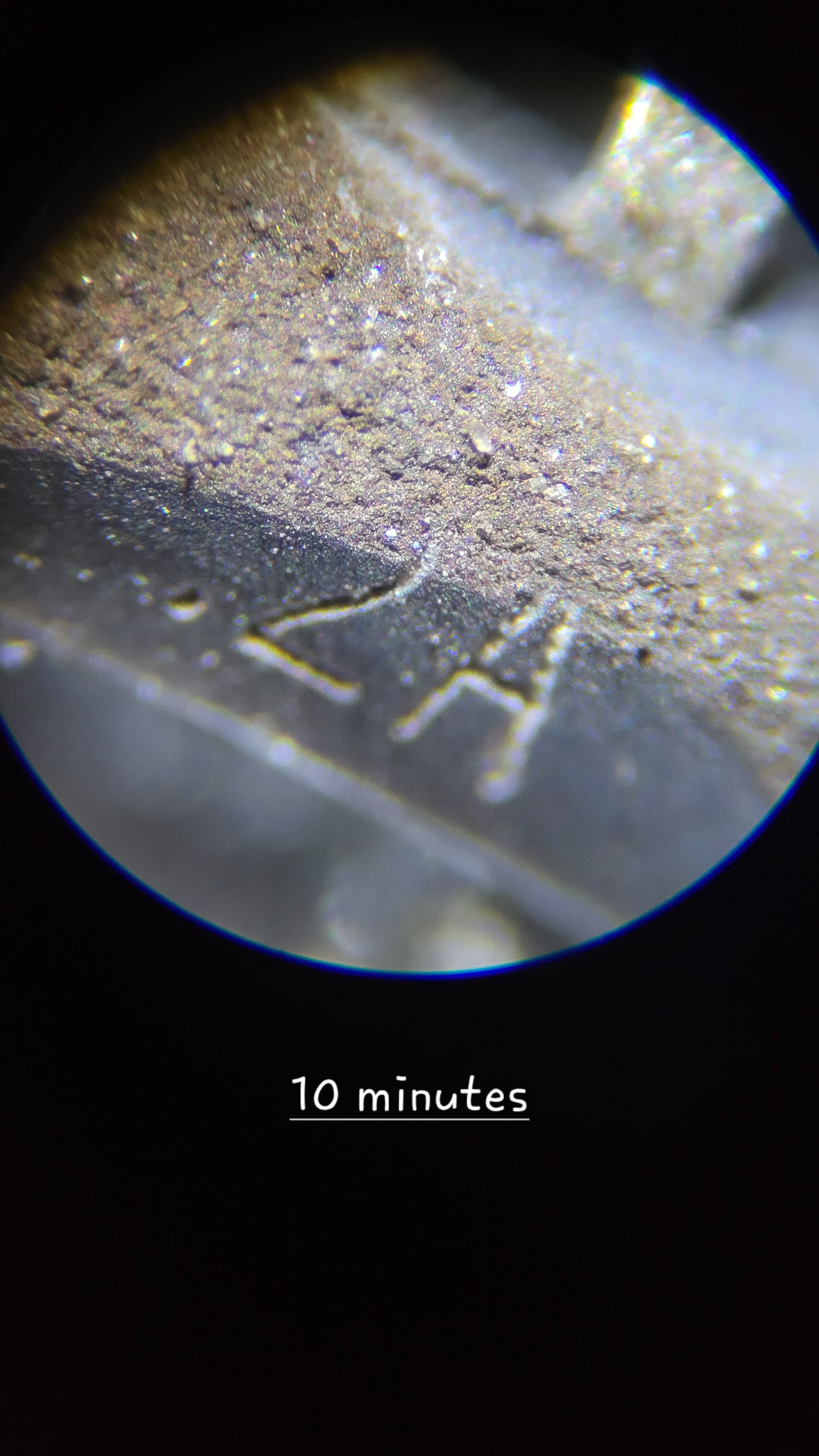
And the preliminary result after 10 minutes of etching
![]()
After some trials
![]()
Even more wire exposed. I am doing it baby steps. I don't want to fry anything.
Here some pics
![]()
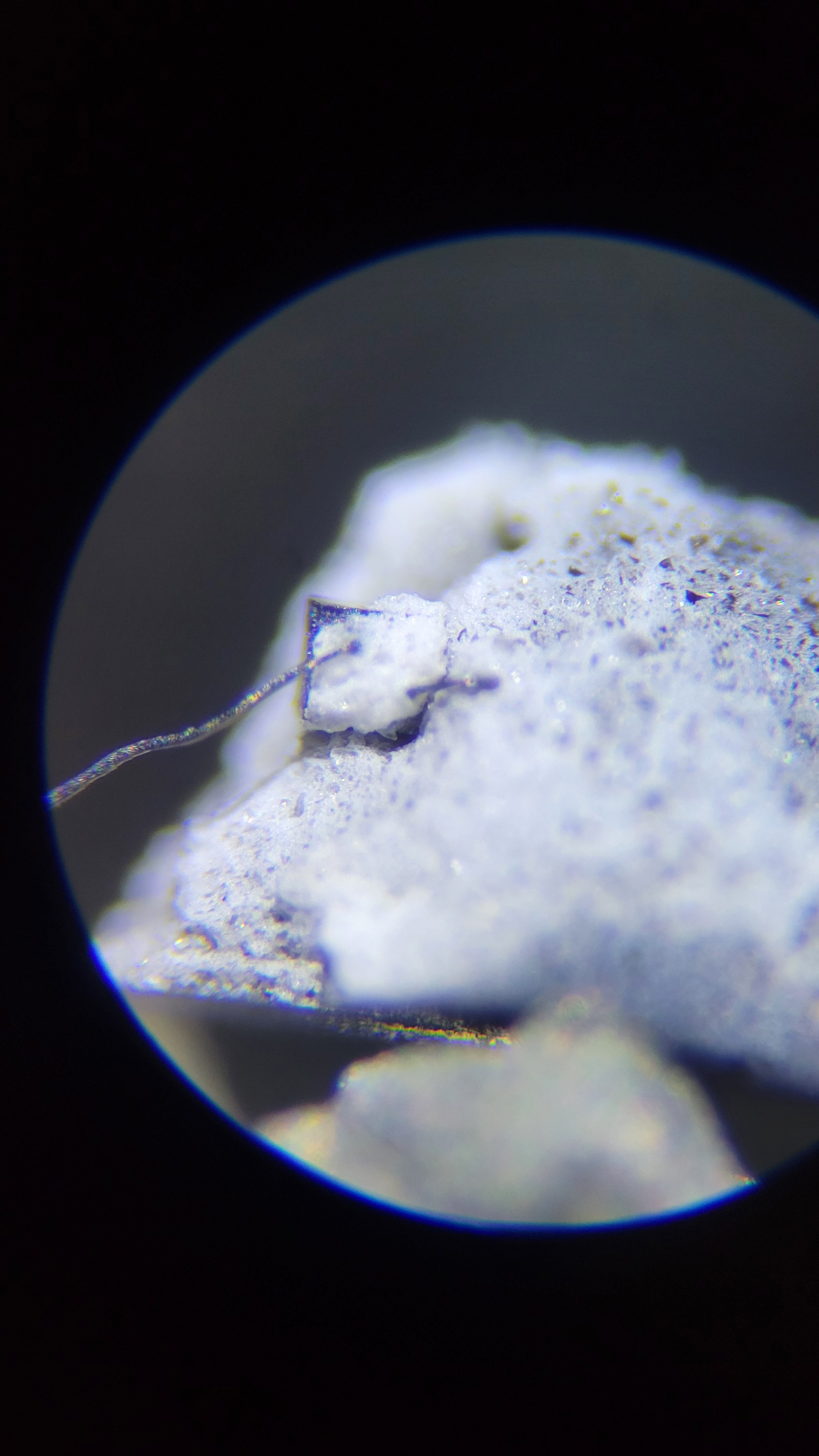
After even more baby steps I got this
![]()
The cube have the transistor we saw earlier.
I don't know how to get rid of the residual on the cube. I've tried ultrasound bath but lost the cube.
-
First trial
11/18/2023 at 14:24 • 0 commentsI got an interesting idea instead wasting time on removing upper layer of chip, why don't we use SMD version. It's really thin encapsulation, it will save tons of time. For standard one we could use laser or cnc to remove upper level.
So, here is our victim
![]()
This was not a good idea as the air passed near the PCB. The next trial I've used one with holes in it.
All clear fire down the hall:
It's looks like it missing the target but it's only because it really above. From side it looks ok.
![]()
Too close to plasma and it burned the PCB a bit.
So there is three parameters here the flame intensity controlled by voltage. Air flow speed controlled by fan speed and tray height.
Once all set you can just seat and drink well deserved tea.
Instead of cleaning the burned residue with hands/tissue or screwdriver I've used ultrasound cleaner to gently remove all necessary and hopefully leave bonding wires where the are.
Fingers crossed, I will continue today. I prefer to take my time and do I right.
I had a problem with this setup, the blowing air can easily blow the plasma off and this apparently may damage Tesla coil. 😭
-
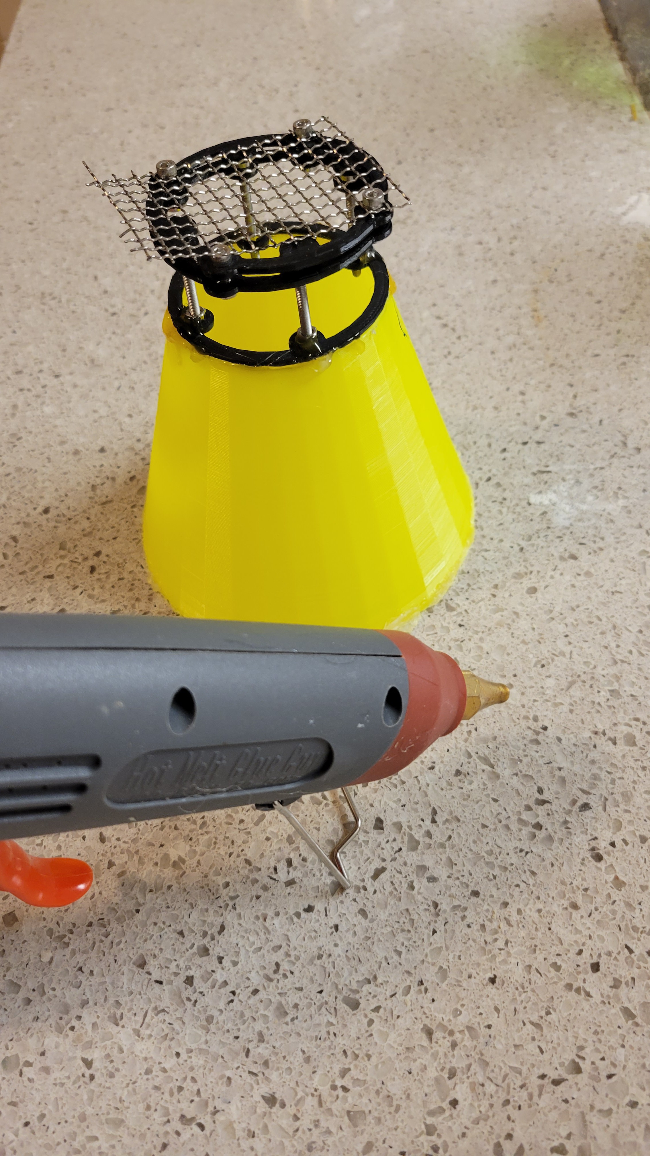
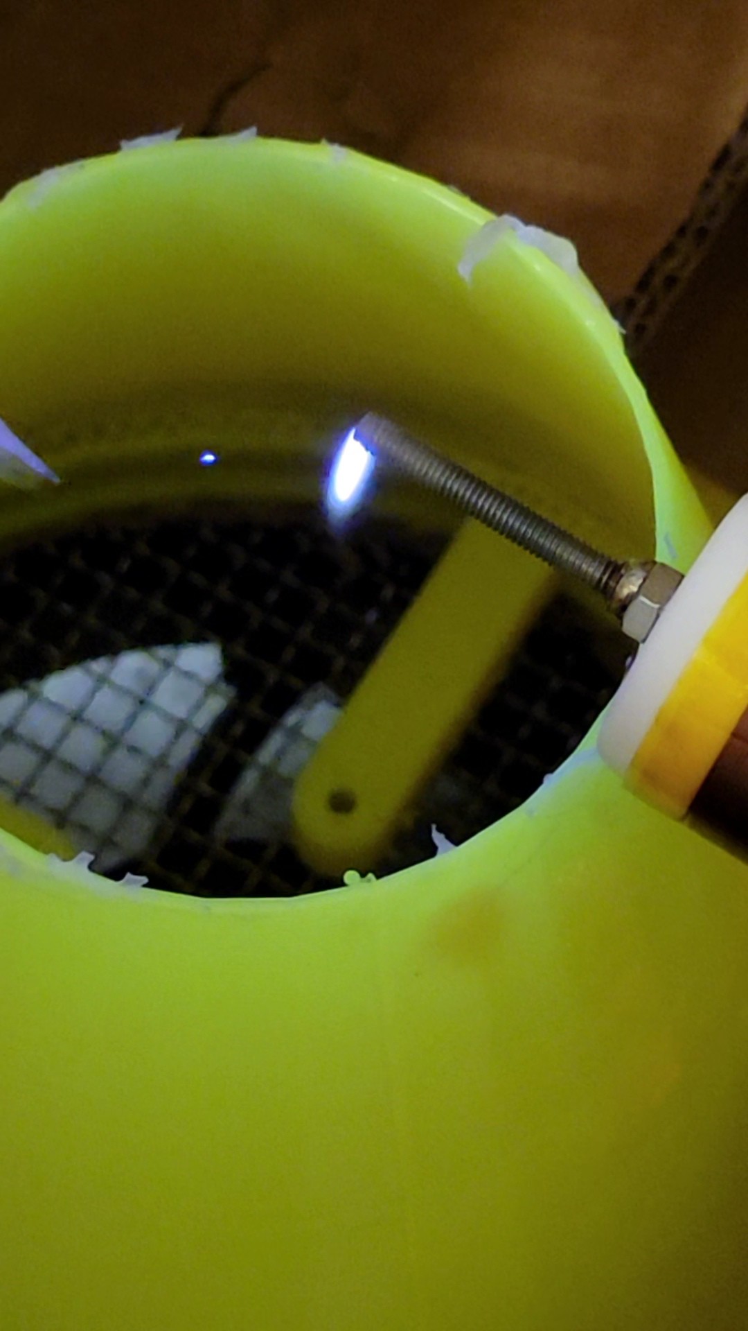
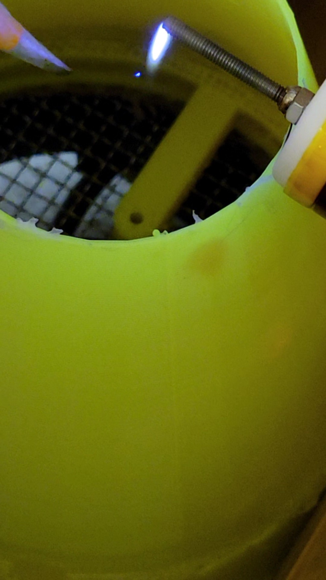
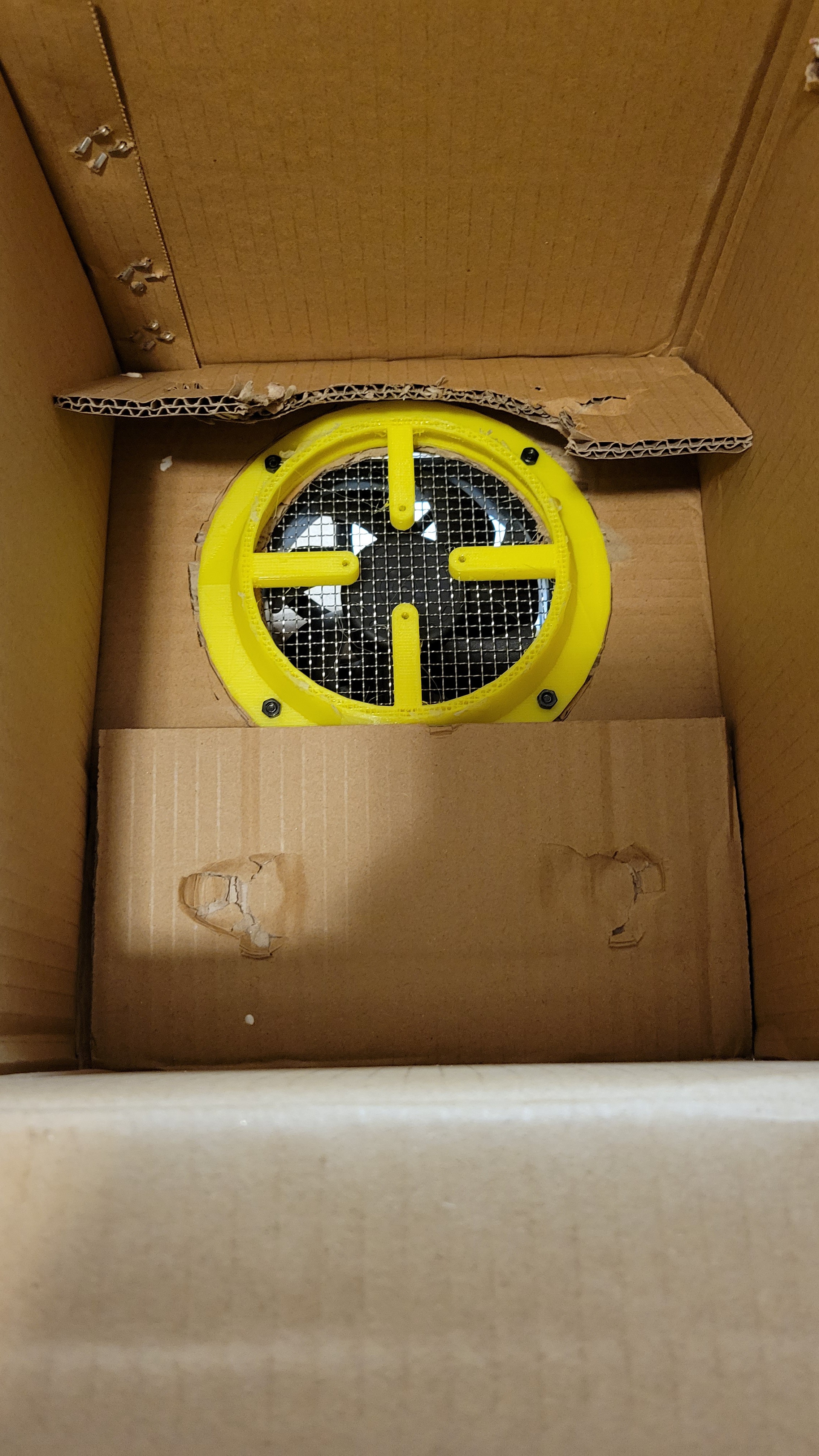
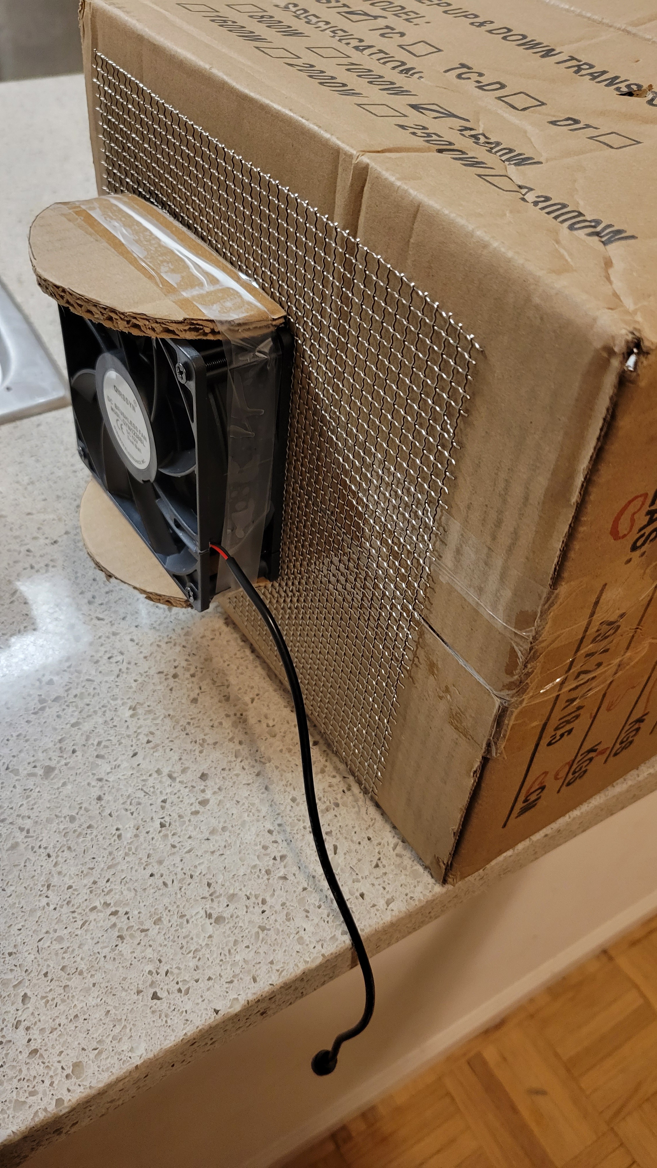
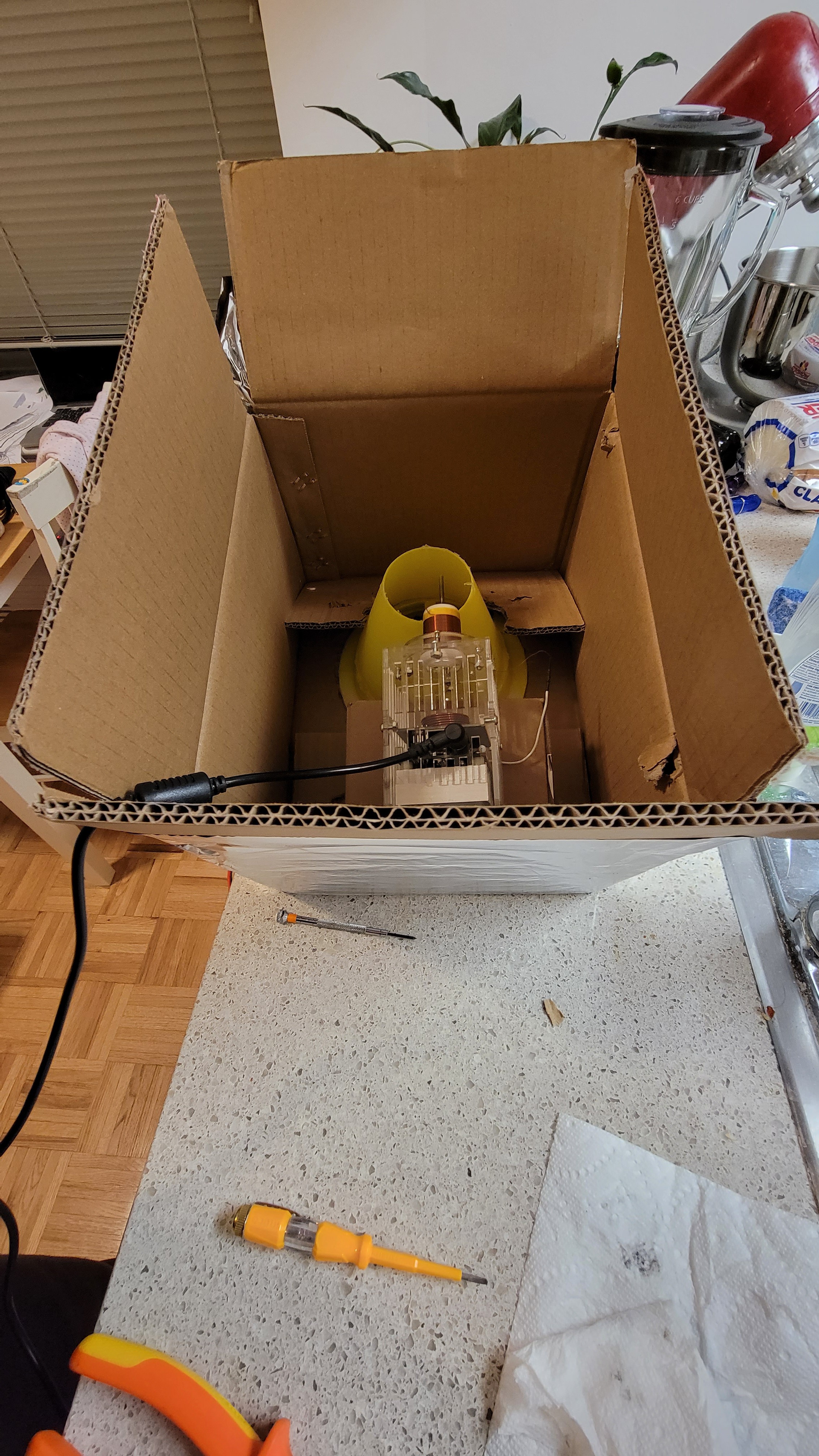
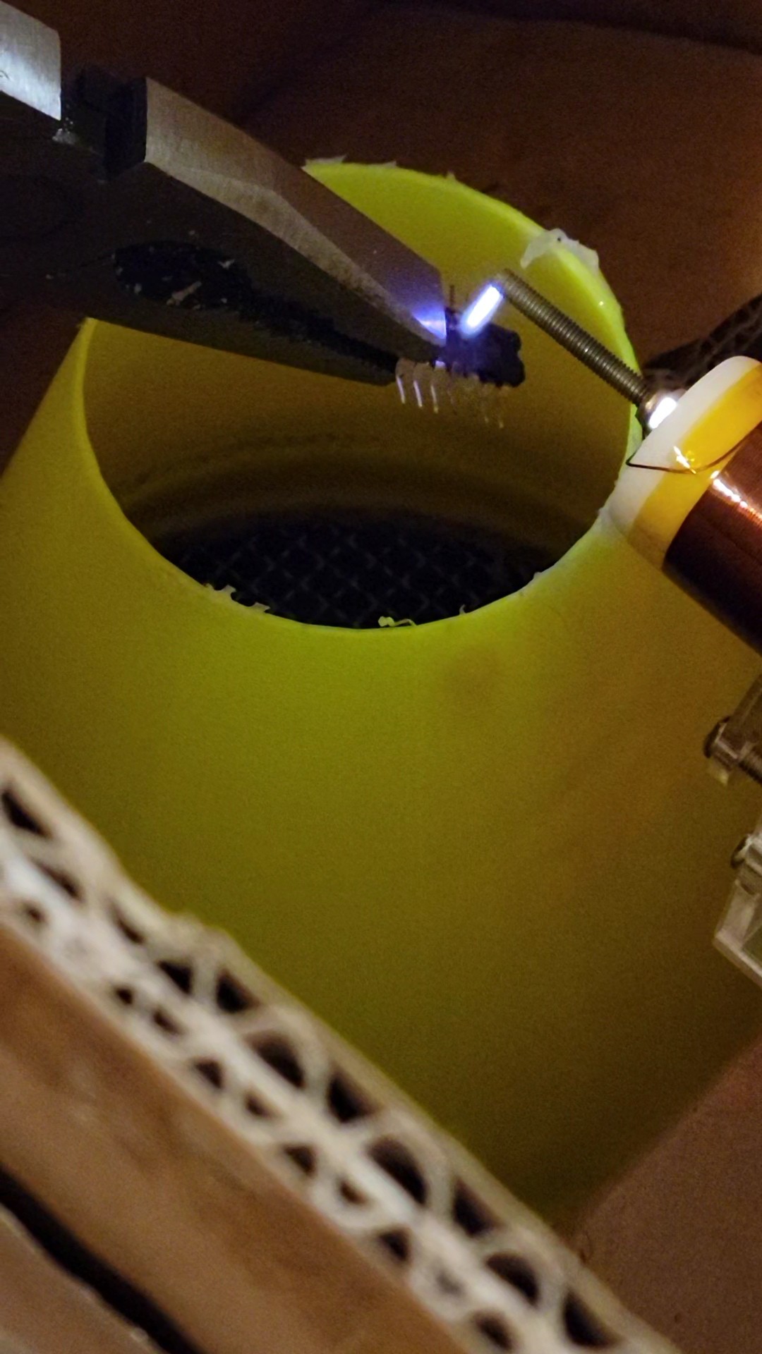
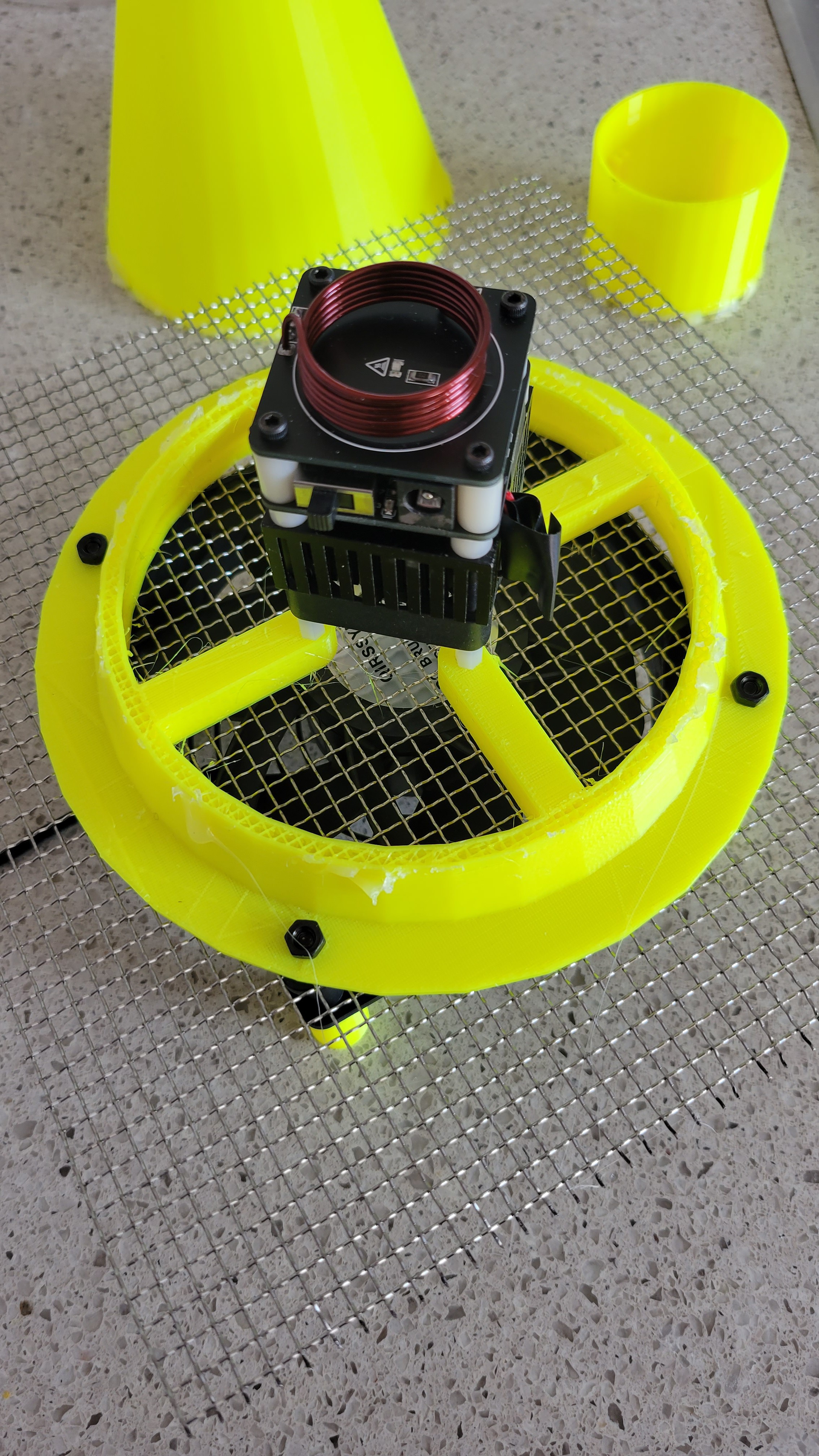
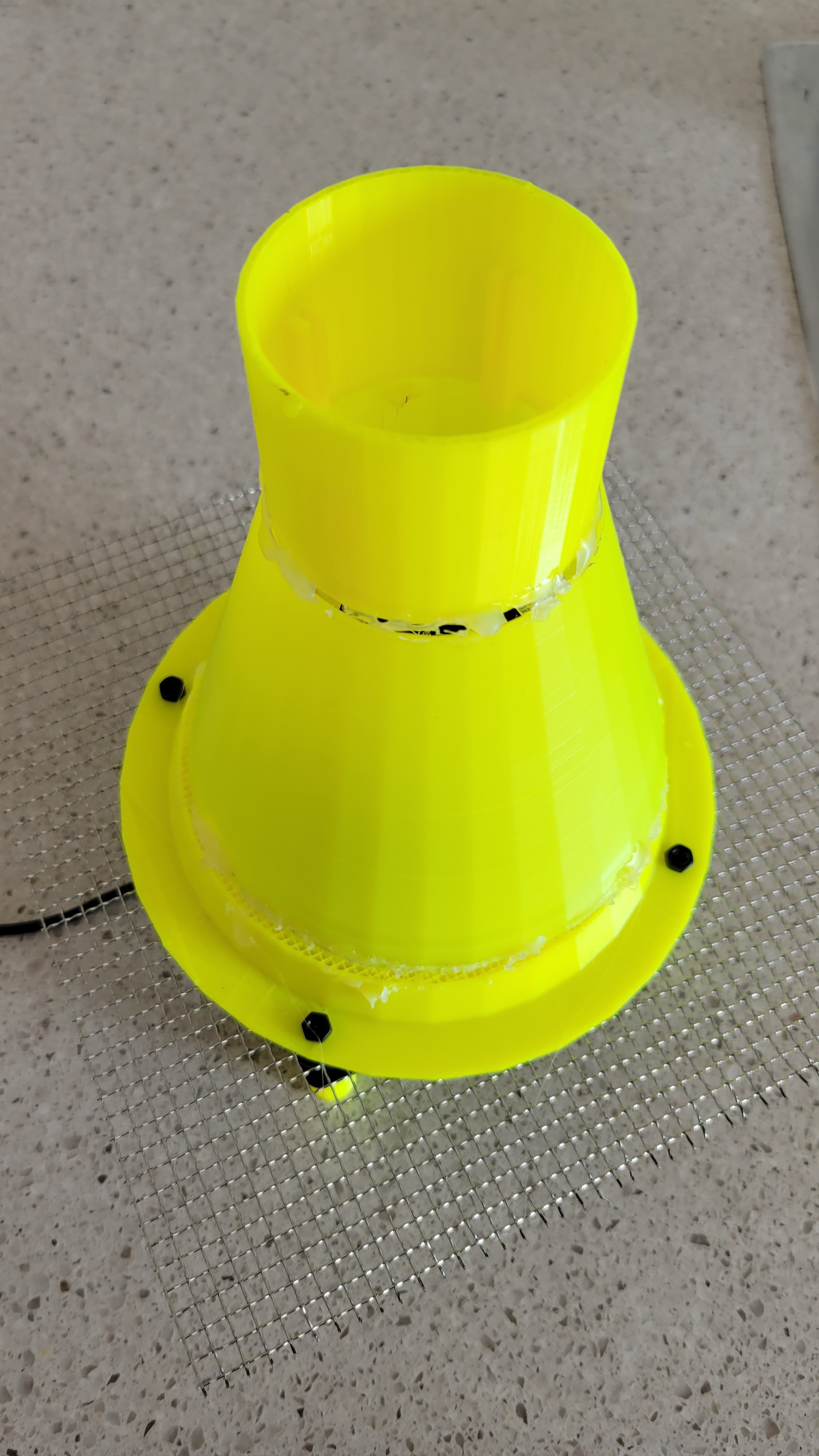
Automatic decapsulation chamber
11/13/2023 at 02:52 • 0 commentsThe idea is to make a box with Tesla coil that produces plasma powerful fan that could control plasma shape and Faraday cage to hold all the energy inside.
Let's start with a box it has a side window to see how far plasma from the chip. Upper opening to let air in and lower opening to let the air out.
![]()
Inside we have a metalic tray that could be height adjusted.
![]()
Trial run looks good
-
Bonding wires
11/06/2023 at 05:20 • 0 commentsAll my exposed silicon were without wire bonds. Wire bond is this thin wire that connects IC to the package. And the question is have I removed them accidentally when cleaning and removing package or it was blown by the high voltage of Tesla coil. To check it I took fine wire I have of 0.0005inch which is 0.0127mm. And put it near by Tesla coil output. You can see it start to glow at distance of about one centimeter.
![]()
And those are a bad news since this means I cannot use plasma to open IC's encapsulation without damaging bond wites, thus leaving IC unfunctional.
But, another test shows that while putting wire near tesla coil is bad putting it near the flame is fine.
![]()
Although more tests are needed to find which distance is minimal. The fact that plasma flame doesn't burn bonding wires is excellent news, now we can hope to extract ICs intact.
-
Let's give it another try
11/01/2023 at 21:07 • 0 commentsI suspect that last time the problem was shielding that was too close. So this time, I used a box wide enough to not create capacitor between shielding and components.
![]()
Placed went to cool it down
![]()
Made EM shielding using aluminum foil. Placed cone to concentrate air flow. And used more heat resistant Tesla coil
![]()
To speed up the process I've filed the IC package where I thought silicon should be (usually in the middle of the package)
![]()
![]()
Now for the fun part... PLASMA!!! That's a good place to warn everyone that you should NOT touch plasma with your hands or conducting material. Use ONLY shielded tools
![]()
It still manual (I am testing some ideas how to make it automatic)
And the result:
![]()
In the middle you can see silicon. Now let's look on it under the microscope
![]()
This time I got lots of residue left. I've tried to use more plasma but eventually silicon popped out and I was unable to find it. I guess I should use ultrasound bath next time.
Here is another happily extracted silicon
![]()
-
Cold Plasma Era
09/15/2023 at 18:55 • 0 commentsBoth in article about microwave induced plasma etching and Tesla coil device I bought (with which I successfully etched few micro-controllers) it got few cm of plasma flame. I though it necessary to use powerful plasma generator. While I was working on my previous project of Tesla coil trying to increase the power I was shocked to find that all this power is unnecessary.
One of main problems with powerful Telsa coil flames was, that it instantly burned the IC's encapsulation and made a real fire. So I had to stop the process stop the fire cool the IC, and after a few seconds it would happen again. Low power Tesla coil on the other hand, didn't burned the IC's encapsulation it gently etched it, leaving clear white mark. It solved one of my big problems about this project of how to keep it safe from burning.
-
Disaster
06/06/2023 at 20:03 • 0 commentsAfter initial success I thought of better way, more automatic.
So I've built structure (that holds Tesla coil and powerful fan) and shield that will hold and cool Tesla coil and won't let radiation escape
Basically, it's a 3D printed cone with aluminium shield on it (not in the picture, already removed it)
![]()
![]()
The problem started once I've grounded the aluminium shield. Something went wrong, before I know it device went kaput.
Well, I've replaced burned IRF250 and tried again making sure everything is far enough from grounded shield. It work for a minute much less powerful than usual and burnt again. I've changed MOSFET again, each time it was worse than previous ...
Arrr...
I guess the grounded shield changed capacity of resonant circuit
-
First attempt
06/06/2023 at 19:41 • 0 commentsTo remove capsulation I used this small yet powerful Tesla coil.
![]()
After about two hours (yeah, too much time in my opinion) I managed to remove epoxy from Atmel's Attiny85.
There are few problems with this aproch:
- First the output coil gets real HOT just after few minutes. So I had to let it cool down.
- If you get the chip to close to the flame it burns get too hot if its too far away nothing happens
- Fumes are terrible
- Radiation is illegal
Integrated Circuit decapping without acid
IC are amazing, but always closed in eopch which seems impossible to remove. Here we propose a method to decap without acids