-
1Solder The Flattest Components First (resistors / diodes)
-
resistors
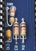
and diodes soldering the standing resistor R6 last (this is the E
Clock pin resistor)
- you can lay R6 Down sideways like this:
![]()
-
resistors
and diodes soldering the standing resistor R6 last (this is the E
Clock pin resistor)
-
2Solder the bypass capacitor
followed by the small bypass capacitors (these are not polarized and go in any way – they are all the same value)
-
3Solder the chips which are under the sockets
then soldering U11, U4 and U3 (these are the two transceivers and the bank register). These must be soldered without a socket, completely flat to the board. Very likely if you make a mistake here it will be very hard to check as these chips are underneath the two 40 Pin DIP packages and can not be placed in a socket.
-
4(depreciated) Close the Jumper Pad
Solder the tiny pad jumper on the board that is labeled “please close for normal operation” if it is not already closed on your board. (this should be fixed on the newer boards but some of the initial run boards that I sent to developers wanting to help require this step). The current recommendation is to take a resistor leg and lay it across the pads with a little dab of flux to hold it in place long enough to join the two pads.
this is pre-closed on 4.2
-
5Resistor packs
Resistor packs next – Please pay attention to the specific pin out and value of each resistor pack. Soldering these in the wrong way or using the wrong value will result in a non-working board.
-
6Decide on orientation for module connectors
Depending on if you want the edge connectors for the serial chip and the SD card module to lay flat you may want to solder these before doing the next step. Future expansions may rely on these being sideways laying down on the side of the board so it might be a good idea to do it this way.
(the below is resolved in REV 4.2.)
Note: to get the SD card interface to fit with larger standoffs it is some times required to trim the screw hole corner on the PCB with tiny side cutters into a square so that the connector will seat properly
-
7Install Required Sockets, Decide on Optional Sockets.
Next sockets you would like to use. You can socket all of the chips but technically only have to socket the CPU and the Atmega32. I highly recommend installing a socket for the the very sensitive RAM chip. I don’t recommend turned pin machined sockets for the CPU, controller or the ram chip as many of these come with additional cross pieces and may not sit tall enough for the chips under the main IC packages to completely clear the bottom of the installed 40 pin packages. Instead use a good High quality “double wipe” spring socket without a cross piece. You can carefully trim a cross piece from the center of the socket so that it neatly fits over U11, U4 and U3.
-
8Taller Components, Socket IC's
Lastly solder the remaining taller parts in any order that suits you. Once all of your sockets are soldered use a multi-meter to check for bridged pins and shorts between pins, especially power and ground. Use the schematics to verify pins that are supposed to be soldered together. Do not forget to close JMP1 if you are going to use the USB dongle for power. Lastly Socket any non soldered ICs.
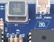
Pointer, The crystal package has a non rounded corner, which needs to line up with the corner on the PCB footprint. Like this:Note that the arrow point's pointing at +5V on the package and not at Pin 1 If i spin a new revision of the board I will remove this marking from the board.
-
9Programming the Microcontroller (Getting Ready)
If you per-purchased a programmed Arduino OR a kit. Your controller should come programed and ready to boot the BIOS.BIN image on a prepared SD Card. So the following is only needed if you are scratch building a kit and sourcing your own parts. These sections are also good for if you for some reason have to (in the rare case) re-flash your boot loader. You can also reference the "Flashing the firmware" section to learn how to update the firmware.
The atmega32 is an integral part of the chip set for the hb63C09, and handles all of the IO processes. Without programming this chip there is no way to stage or boot the computer. And while this is not dif
le this)
To set your system wide serial port:
ficult, it is an important step which must be completed after soldering the PCB together. For the time being a small ISP programmer (or another Arduino) is required to flash the atmega32’s programming to the chip. There are many guides on the internet for using an Arduino as a programmer, so here I will lay out using a USBtiny programmer
-
You will need a USBTiny
programmer like this one from Amazon (or similar):
- https://www.amazon.com/HiLetgo-USBTiny-USBtinyISP-Programmer-Bootloader/dp/B01CZVZ1XM
- TinyASP is also verified to work with an 8 to 6 pin adapter.
- You will need a FTDI or TTL to USB adapter with DTR or RTS. The pin out is configured for the FTDI FT232RL adapter like this one:
-
You will need Arduino, freely
available from:
- https://www.arduino.cc/en/software (I prefer the legacy version but the newer one should work too)
- you may also have to set up “dial out” to make programmers and serial to usb converters work under linux. Directions for this can be found here: https://support.arduino.cc/hc/en-us/articles/360016495679-Fix-port-access-on-Linux
-
You will need to install
Mighty core:
- https://github.com/MCUdude/MightyCore (directions for this in the repository)
-
You will need a USBTiny
programmer like this one from Amazon (or similar):
-
10Setting up Arduino to Flash the bootloader
After installing / obtaining the above you will need to select the chip This can be found under:
Tools → Board → MightyCore → Atmega32
And then Selecting the clock speed of your crystal oscillator:
Tools → Clock → External 20Mhz
Lastly Check your programmer is selected, for USBTinyISP pick:
Tools → Programmer → USBTinyISP (slow)
you may try “fast” however, I have noticed that the “slow” selection causes fewer issues over all.
HB63C09M - 10x10 HD63C09 Based SBC
This is my project page for my new home brew computer, a multi-processor 63c09 and AVR SBC.
 Dave Collins
 Note that the arrow point's pointing at +5V on the package and not at Pin 1 If i spin a new revision of the board I will remove this marking from the board.
Discussions
Become a Hackaday.io Member
Create an account to leave a comment. Already have an account? Log In.