-
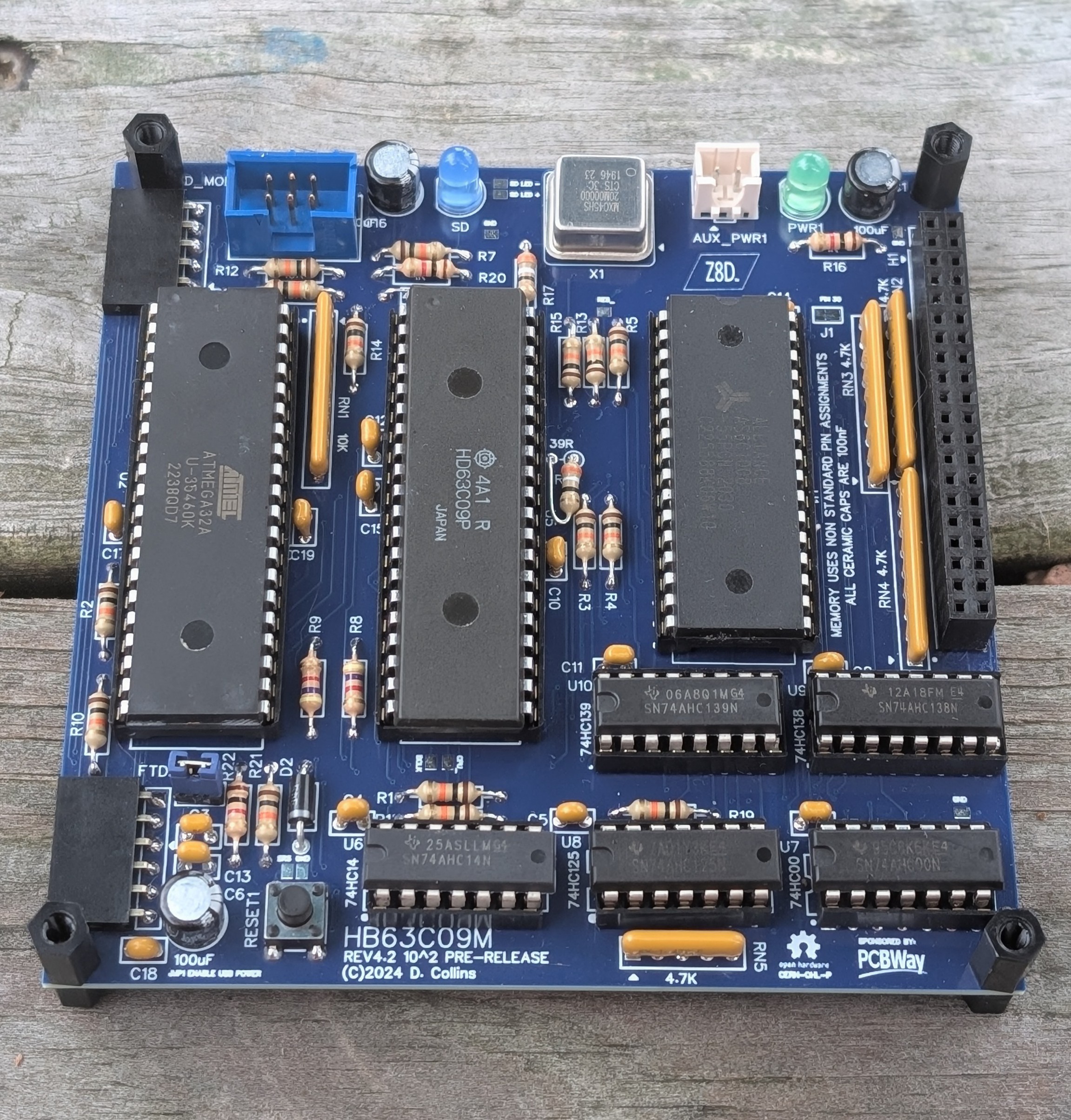
Rev 4.2 Form Factor change, Project release!
11/04/2024 at 20:15 • 0 comments![]()
Intro and Forward:
The HB63C09M was an idea I hatched back two years ago when I was finishing up my first home-brew computer the HB6809. But it goes back further than that. The beginning is really around 2020 when I started building kit computers as a means to pass the time during the pandemic. I had purchased a kit from McJohn in Italy called the Z80-MBC2, by Fabio Defabis – an excellent little computer kit with a single logic chip, atmega32, Z80 CPU and a RAM chip. I was hooked on the small form factor and the things that I could do with my little computer. I made a few hardware expansions for it, most notably a joystick interface for my Tetris clone that I had programmed in pascal. At the time there were people asking Fabio on the Facebook group for the project if he was going to do other processors. Before long he was working on the V20-MBC (which I built) and later he went on to make the 68K-MBC which is architecturally slightly different. After a while, no new MBC computers were made, and by then I was on to building my 6809 based system, and still quite a novice at this (I am still!)
Things happened life got busy I spent some time working on other projects and about a year ago started playing around with Arduino – and digging very deeply into the Z80-MBC2. I really wanted to understand how memory was loaded using a microcontroller and I wanted to know how Fabio had shared the bus with the Z80. Right around the same time I had also stumbled onto an even older work, Brad Rodreguez’s “Scroungemaster” and I fell in love. The scroungemaster is (well was) a concept for a 6809 multi-processing build Brad had built on wire wrap. He had used a rather simple circuit to do clock stretching in order to hand off cleanly to the other CPU’s into common ram. He detailed this in a paper entitled “Multiprocessing for the Impoverished” (found at https://www.bradrodriguez.com/papers/) I quietly started to play around with the design and build a small expansion for the HB6809 that allowed me to use an Arduino like a peripheral without a latch simply by stretching the clock.
In his paper, Brad discusses the parallels between the Z80 and the 6809. I found a lot of parallels in my Arduino sketch and the work that Fabio had done with the Z80-MBC2, and after a few months I had a working prototype that could stage itself from the Arduino (at the time using latches) and boot into a machine language monitor. After that I streamlined the design, making it slightly more like the Z80-MBC2’s little brother the Z80-MBC by opening up a few address lines to the Arduino and then additionally solving a very difficult timing problem by changing from a controller generated clock to a synchronous clock (both the 63C09’s internal clock and the ATMEGA32 are clocked by the same 20Mhz crystal) and the board fully stages from ROM files saved to the SD card. No Rom code exists on the AVR EEPROM (save a small less than 40 byte program that bootstraps from the SD card). This allows the programmer and user to switch between environments without having to Flash a ROM onto the computer!
After a few revisions of the board, I found I could further shrink the form factor to a smaller 10x10 PCB – albeit 4 layers. The Exact same size PCB as the Z80-MBC2! For me, it was like coming full circle, and now I think I am ready to share this design with others. What I have is a fully functioning – ready to go 63C09 playground. But there's still some work on the software, this is where you come in.
What I am calling this board revision is “The Prerelease” edition. Essentially the hardware is finished. From this point, any and all architecture changes will need to be approved by the “Community” -- what that means specifically will have to depend on the group of developers that go ahead and early adopt the design for the express purpose of porting software to it. For now there is enough (really) for people to start playing around with the platform in earnest, basic, machine language monitor are all there. I have started this document which is a rough outline of a manual for programmers and developers. But to really go forward I need somebody who’s more versed in operating systems than I am. I could possibly figure out how to continue developing software and add LBA device support to basic and possibly the monitor – but I would very much be learning as I go. So The main purpose of this release is to get the boards out there in to peoples hands, hopefully people with considerably more systems knowledge who have a passion for the 6x09 CPU and can really take the lead on developing things like FLEX, Nitros09, Forth and hopefully a lot more!
Resources, How to get started:
Some files are here in the files section, however most up - to date info is always going to be on the Github Everything including the BOM and Gerbers for assembly is available there. If you are confused or need a hand with something you can try the Facebook page. There is a brief programmers reference, that goes over accessing devices as well as the memory map. A short step by step assembly guide can be found in the programmers reference, and here which includes programing the bootloader as well as programing the firmware onto the MCU.
What if I want to help:
Email me at Z80Dad@Gmail.com and we can talk, I'd be thrilled to help you get a board into your hands, and I can offer boards and kits cheaper to people willing to help develop software. I have a very small number of boards and parts left over from development, and would like to put those into the hands of hobbyists or developers. Right now I am trying to see how that looks. I have a few that I promised to some of you already and have began sending those out. In the next few days I'll be putting together a Tindie storefront and ill make some boards available there once I've verified how many sets of parts I have. Honestly - building the board up from scratch isn't so bad. Its about 44 dollars worth of parts shipped (not including the CPU and the modules ), the PCB itself is approximately the same price from PCBWay (for 5 PCB's - the down side of this is then you have 5). I want to find a way that makes sense for people to do a group buy ... that might be the best way to get this started, so in the next few days Ill post something up on the Facebook group to all who are interested in a group buy to see what that looks like.
-
Sharing the bus with an Arduino without a latch
01/21/2024 at 02:09 • 1 commentREV3 Works and synchronization scales exactly as expected!
![]()
In short, the REV3 prototype is running at 20MHz. All of the underlying functionality is synchronizing, scaled up from 16MHz with zero issues. I am ecstatic and want to thank PCBWay for getting the prototype to a stable state by again covering a 2nd run of the mini ITX PCB. They have always been a wonderful partner in retro and I would not be able to operate nearly as quickly as I do without their help.
The problem of the REV1 Prototype:
What we learned from REV1 specifically is, using the AVR to Clock the CPU is bad because we don’t know (inside the context of the code) where the CPU clock is at when we send the IOGNT_ signal as it is interrupt timer driven. Generally the best we can do is guess, and insert a delay (as the AVR in REV1 was clocked at 16 Mhz and the CPU was clocked at 4Mhz). Guessing is bad as there is, turns out – a lot that can happen to delay or decrease the period of time the AVR takes to finish this process. This causes a bit of instability and made it generally impossible to move forward on optimizing things.
How does the AVR share the bus with the HD63C09?
The bus arbitration was switched from active arbitration (REV1) where delays were used to insure the IOGNT_ was held long enough to prevent MRDY from bouncing, to passive synchronized arbitration (REV2 and REV3). Essentially what this means is, both CPU's are using the same system clock and so every 4 cycles they finish their current cycle at the same time. To really understand requires some explanation, This all comes down to the specific timing of the 63C09’s decode cycle.
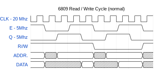
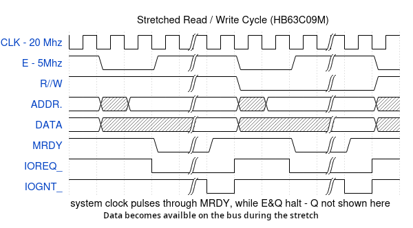
the following timing diagrams snap to the system clock, this is to show how the clock synchronization works vs actually showing the nS to nS events, some edges happen just before or after they are drawn here so for simplicity sake - please pardon that inaccuracy. ![]()
The 63C09 creates the quadrature clock’s (E & Q) which are 90 degrees offset from each other. In the case of the HB63C09M these clocks run at ¼ the system clock due to a simple internal clock divider that uses a set of J/K Flip Flops (each flip flop divides by 2). The 63C09E (‘E’ for external) generates this clock external to the chip, which opens up some of the 40 pin package for extra signals which are useful for more traditional bus arbitration. Both CPU’s have the option of using a clock stretching circuit which allows the designer to “hold over” or stretch the clock by up to 5uS. This 5uS limitation is to allow the CPU to refresh its internal dynamic registers to avoid data corruption. I briefly went over this in REV1 architecture overview.
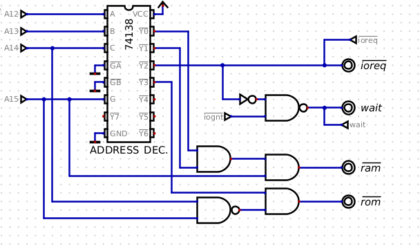
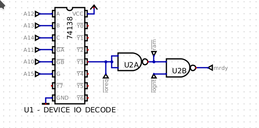
While significant changes have occurred within the selection chip set, the request grant circuit remains consistent. In this circuit, the AVR typically keeps the IOGNT_ signal high, except when it intends to relinquish control of the data bus to the CPU. When the CPU reads or writes to 0xA000 – 0xAFFF, this generates an IO request via the address decoder. Once the IO request is initiated, the address decoder generates a low signal that, after passing through an inverter to one input of the NAND gate, sets the output low as long as the leg tied to IOGNT_ is high. This output is tied to the MRDY signal on the CPU and begins a clock stretch. This state persists until the IOGNT_ signal pulsed low by the AVR for exactly ½ cycle of E.
![]()
REV2/3 Decode / Bus Arbitration Circuit Simple enough right? But what if we release IOGNT_ before the IO Request ends (less than ½ of E)? In short, we would have a problem. Since it’s just a passive logic circuit it would compute the result and pass it along to essentially the MRDY line causing it to bounce a few nS before the IO request finishes – this may trigger a second clock stretch early, or cause other unpredictable things to happen on the busses or inside the CPU which usually just result in a non working system.
So how can we take advantage of clock synchronization to fix this issue:
![]()
The advantage here IS the 5uS limitation – this sounds strange however it is a fixed limitation regardless of the speed of the system clock. The 63c09 can handle ~.6 to .75 instructions per cycle, depending on the instruction. The AVR on the other hand can handle 1 instruction per cycle. Meaning running at 16Mhz it can perform 80 instructions in 5uS, and at 20Mhz it can perform 100. This might not seem like a lot of overhead at first. However, when broken down into single step IO requests like: Send a character to the UART, read the value of a status register, or set the bank register to a value on the bus; you can start to see the advantages. Furthermore, because the AVR can flip a bit on and off in an internal register in exactly 2 cycles of the system clock, we can see that this is exactly ½ of E! So, we can be assured that when the AVR holds the IOGNT_ signal low, it will stay low until just as the address bus is beginning to change. This means the firmware does not have to do any of the timing, as the timing is handled through synchronization.
Furthermore, no matter what happens inside the stretch be it 3 AVR cycles or 90, when we send the grant signal to the request grant circuit, the CPU's will continue on in a synchronized fashion without any worry that things will get out of sync.
SO, putting it all together:
Since each bit flip of IOGNT_ happens on each subsequent system pulse clock pulse, we can predict the amount of time each operation will take as the AVR can flip a bit in 1 cycle. We also know that E is held high and will almost immediately latch the data (in a read), or move on to the next cycle (in the case of a write) after MRDY ends the address bus has moved on. Because of this IOGNT_ will rise synchronous to the end of the IOREQ_ signal from the address decoder. This will happen in such a way, that even after the clock stretch, both CPU’s will still be synchronized. Furthermore, because both CPUs are tied to the same clock the result is exactly the same (within the maximums), whether or not the clock on the AVR is running at 4Mhz or 20Mhz. No state machine, no fuzzy timing math, no latching the data to later grab it off outside of real time; no running the MCU 300-400x the speed of the CPU to catch interrupts and data in real time. Essentially, to the CPU, the AVR is a regular old slow memory device, and to the AVR the CPU is just an 8 bit latch.
Thank you for going along with me on this journey, I hope that this has given a good groundwork for understanding the inner workings of the HB63C09M. If anything this technique is very easy to replicate and will work on any 8 bit CPU that has a clock stretching mechanism. Furthermore, the fully static Z80 and 6502 would not have to even worry about the length of the stretch period which opens up some very interesting options for sharing the bus.
For those that are interested I hope to have the design files in a state that is ready to share by the next revision or two, until then the design schematics are always available in the files section here. In addition I did a hack a day pages piece on how the mezzanine connection developments are going, if you'd like to check that out it is linked here.
Have a wonderful week, I will keep everybody up to date as things progress.
-
REV3 Prototype chipset overview
01/04/2024 at 19:58 • 0 comments![REV3 Board REV3 Board]()
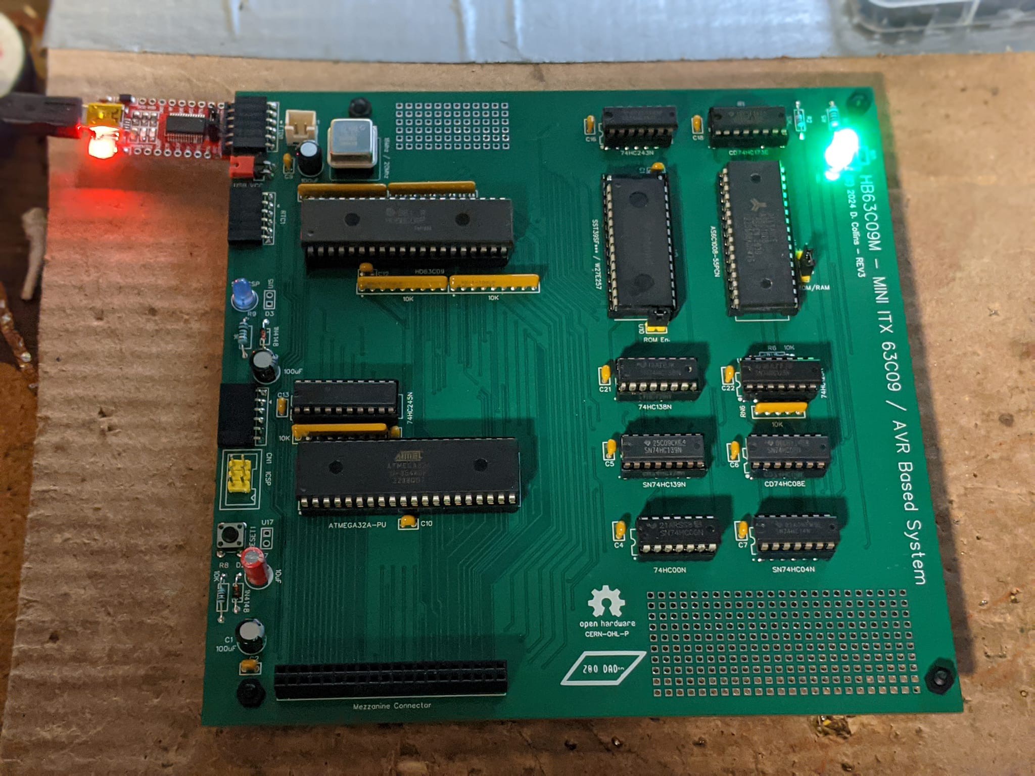
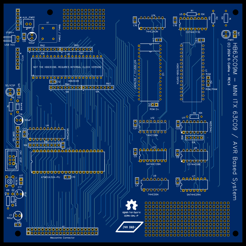
REV3 Board Render (top) The Rev3 Board is basically a copy of the hand wired Rev2, itself a retrofit HB6809. The Hand wired prototype (see below) was more or less the new chip set design, along with a very stable pierce oscillator I built in about 2 weeks time working nights. What was accomplished with the REV2 build was considerably faster clock, which clocks both the 63C09 and the AVR simultaneously at 16 Mhz. The plan is to push the Rev3 to 20 Mhz. In order to do this it was clear I had to make some tough choices about the chip set. Looking back at the failings of the REV1 board, one of the biggest issues was chip count and latency. These things didn't matter as much on the breadboard prototype as it ran an asynchronous clock (similar to the Z80-MBC2) with the AVR clock coming from a crystal oscillator, and the AVR it's self clocking the 63C09 at 1/4 to 1/2 it's clock. But when I translated that design it didn't seem to work well on the PCB. This coupled with several mistakes made while documenting the Big mess of wires breadboard, and in the actual routing mistakes the whole board was more or less a non starter.
![]()
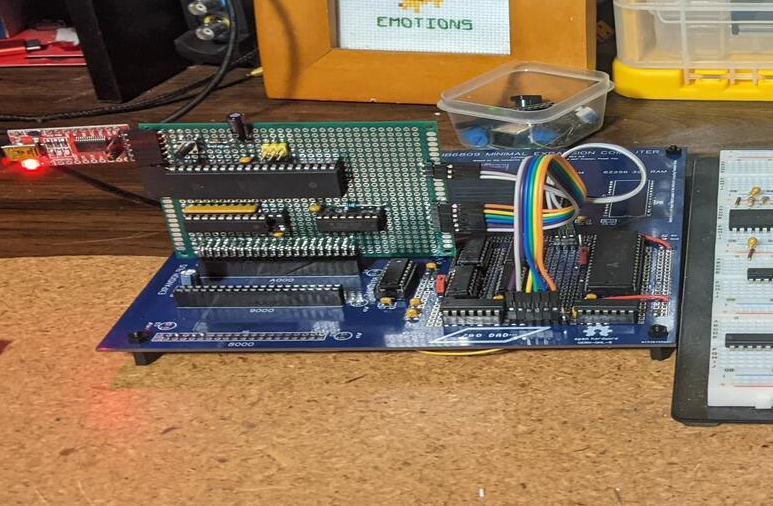
REV2 hand wired board What I learned from the REV1 board is to fit all of these components comfortably on a Mini ITX motherboard, I needed to reduce the chip count to make all of the connections fit (or go to a significantly more expensive multi-layer board). In order to do this I had to significantly reduce the chip count, and in the case of the bank selection circuitry I further reduced the space the chips take up by both simplifying the the design and choosing different parts. A few of you have commented that it might be simpler to just roll together a custom ULA for the design. I think that this makes a lot of sense, but the trouble with that approach is that it may become harder to find CPLD / GAL parts as replacements. This is not the case using standard 74 series parts, and as you will see below the design is very simplified to what I could determine as the fewest possible parts to accomplish what was needed.
New memory map:
The simplified memory map made using less logic chips for address decoding significantly more obtainable.
ROM / RAM Configuration Addreses 64K Main Address Space B000-FFFF Upper Fixed Ram 20K Physical Rom Space ( A000-AFFF Device Address Space for MCU and Mezzanine connection 4000-9FFF Lower Fixed 24K Fixed Lower Ram Bank 0000-3FFF Memory Bank Window, set by bank register (16K) 128K RAM Chip Layout 1C000-1FFFF Bank 7 (16K) 18000-1BFFF Bank 6 (16K) 14000-17FFF Bank 5 (16K) 10000-13FFF Bank 4 (16K) C000-FFFF Bank 3 (16K) A000-BFFF Bank 2 Usable – 8K of usable space 2000-3FFF in bank address 8000-9FFF Bank 2 Lower Fixed Ram Bank top 8K of Memory “Shadow” 4000-7FFF Bank 1 Lower Fixed Ram bank bottom 16K 0000-3FFF Bank 0 (16K) system boots with this bank loaded giving 40k cont. “Bank2” selects the ram chip between 8000-BFFF. When this bank is selected, 0000-1FFF (in the bank) will map to the last 8K of the fixed RAM area (in the 64k address space of the CPU). Whereas 2000-3FFF is available for use for programs. Overwriting the bottom 8K will cause data corruption in the top of the fixed RAM area (in the 64k address space of the CPU), As this is effectively the same area on the ram chip.
In “RAM Only mode” the address range B000 – FFFF is physically writable at that CPU physical address as the ROM is disabled. This can be configured on the board by removing the “ROM Enable” jumper
and moving the Ram selection Jumper to “RAM” In this mode the AVR needs to be configured to update the ram from SD at boot. This is not yet implementedThe bank selection circuit was simplified greatly and reduced from 3 chips to 2, using more or less the same circuit as before for address decode. With the added benefit of being able to relocate the system page and various other stacks, along with the reset vectors being hard coded to the top of memory this makes placing the swap-able memory bank at the bottom of RAM ideal so long as the programmer is careful to not swap the various stacks from accessible space.
Bank select chips:
![]()
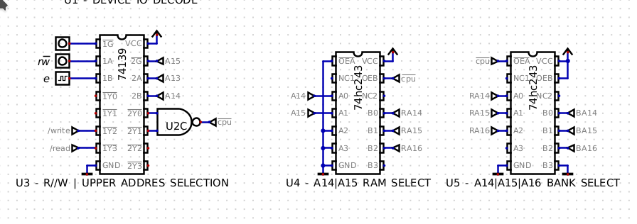
Bank Selection Circuit Bank selection is handled by a 74hc173 (4 bit register) and a 74hc243 (4 bit bus transceiver). Output selection is determined by one half of a 74hc139 (dual 2:4 decoder) and 1/4 of a quad and gate, used to AND the two values from the address decoder and generate the /CPU signal. Each chip is able to tri-state its outputs which are hardwired to the top of the ram chip address lines A14,A15,and A16. While the 243 is set up to output the CPU physical A14 and A15 lines (and hold A16 low) when /CPU is HIGH, the 173 is configured to output its stored logical address values (at the same locations) when /CPU is LOW. The stored value is clocked from the bus with the actual clock signal being driven by a AVR request. Simply writing to an address mapped to the AVR (which sees the bottom 4 address lines) will trigger to the AVR to send a clock signal to the register, which will latch the bank address logical value into the register. (currently implemented and verified working)
The address decoder / request grant circuit:
![]()
address decode add request grant circuit The address decode circuit uses a single 74hc138 3:8 decoder (just like the HB6809), the remaining 3/4ths 74hc08 quad AND gate, and 1/4th of a 74hc00 NAND gate. The logical function of the /ram, /rom and /ioreq signals are fairly self explanatory following the logic gates. The request grant circuit is a single inverter from a 74hc04, and a 1/4th of the NAND gate. This is the same Request grant circuit that is used in REV1. Essentially wait is driven low by sending y2 from the decoder to a low state by writing or reading from the address range A000 - AFFF. Wait is sent to a buffer which has it's output connected to MRDY on the 63C09. This causes the clock to stretch. Meanwhile the /iognt signal is controlled by the AVR, the AVR holds this signal high, until an IO operation is confirmed "done" and then it sends it low for exactly the same period as 1/2 system clock (a benefit of the now synchronized clocks). This is the exact amount of time required to hold wait high until the address cycle has moved on to the next in the 63C09. Some degree of care needs to be taken to assure that the AVR does not stretch the clock for "too long" which is defined by the datasheet as approximately 6uS. It is important to understand once /iognt is asserted the clock stretch immediately ends and the internal registers and instantly refreshed on the falling edge of E (which happens at roughly the same time as the MRDY signal is returned to a high state)
Tri-state buffer:
The sixth and final chip is a 74HC125 Tri state buffer. This chip handles the various signals such as the IO request signal in the case of a mezzanine request, the various read and write signals as well as holding the MRDY signal in a high state during system reset (as the grant circuit is not configured by the AVR during a system reset).Next steps:
Next is waiting on boards from PCBWay which should come next week some time, I still have to spend some time testing a few things on the REV2 board in the meanwhile such as handling the mezzanine requests. The eagle eyed among you will have noticed that AVR has to do some work to roll over the grant signal in this case. Once the boards arrive, some time must be spent putting them together and testing the additional features. One of my concerns is handling the SD card requests in a timely manor during the 6uS window. I have a few ideas for this but would be interested in hearing someone else's take on that. Once I have the SD card up and working I will need to work on a bootstrap loader for the RAM only mode of the board -- this will involve writing a small machine language program that can be handed off to the CPU at boot time one byte at a time - this is exactly how it is done on the Z80-MBC2 and can be done in almost the same way on the 63C09.
-
REV1 PCB Pitfalls, whats next?
10/21/2023 at 21:30 • 0 commentsReflections:
General reflections from last time
Well you read the title here, so its not hard to guess what the outcome from the first PCB run was. In short, the 1st PCB design has issues.
![]()
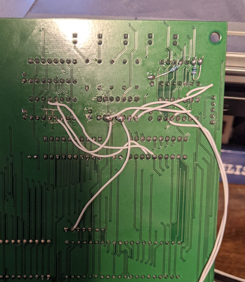
I tried working evenings for the last week to get it to come to life, however there are a ton of stability and possibly further routing mistakes that meant that all scaled into very bad ringing, noise and timing issues. To be clear, none of this is the manufacturers fault. All the issues and pitfalls in this design lie solely on my shoulders. I have plans to fix the issues, but its going to take some time and a step back to really understand the problem.
What is next?
I want to take a step back and look at the design in pieces. I still have a handful of boards left over from the HB6809, There's ample prototyping space on there for me to experiment with. This weekend I want to start by building a very simple but very stable Pierce oscillator, and see if I can get the CPU, RAM and ROM to come up on a 16Mhz base clock. Once this works I will work to add subsystems and to a much better job of documenting the build up as I go.
On the firmware side over the next two weeks I want to focus on getting the RAM to stage on the breadboard build without using the latches. I think I can use the CPU to stage it's own ROM space by feeding it one byte of machine code at a time running in peripheral mode (I discuss this in the architecture overview) . This will further get the chip count down, which is important because the end goal is to have a computer that is built on 10cm x 10cm boards (or less) and currently they are 170x170 so we need almost a 50% reduction, or to switch to a mini frame design with expansion headers that link the boards together. I also DO still want a 68C09 motherboard that just drops into a PC case, because that was the whole idea in the first place, but a lower cost version would also be nice in terms of making the design more accessible.
PCB review how they hold up to rework:
Speaking of the PCB's, I wanted to share my thoughts on the boards produced by PCBWay, what you get in terms of cost for a large format board like this as well as what it's like to rework a two layer rapid turn PCB like this with manual tools.
First, and I've touched on this before, PCBWay does a higher than average job on masking. If you wanted to make a short run of boards with ENG or even Lead Free HASL, for commercial sale these boards really do hold up. Nothing peels with normal handling, and it stands up to even the highest level of abuse. The edge finishing is top notch, nothing is left with a sharp edge (unless you specify that, of course!) and I never felt like if I handled the boards without gloves that I would be cut or that the edges would catch on the work surface. Other manufacturers in China do not take the time, as PCBWay does, to really get this right.
As an example, the 14 pin socket had to be completely removed to rework trace mistakes that were made in the design files using just manual tools (which always require a level of care), I was able to remove the socket and replace with only minimal mask removal, and all of this was around pins which tie into board planes. If I had a a reliable way to preheat the board none of this would have even been an issue given the finishing on the PCBs.
On average, PCBWay is more of an expense. But all of these touches are a value add, and I believe given the blazing fast turn around to North America, the quality really is worth the expense. I would have no problem recommending them over the other producers in China, they do a great job with what you pay for. Additionally they don't over charge for shipping and have several options depending on your required turn around (which all obviously scale with the price.) They also continue to offer a low price on 10x10 PCBs that matches all the other sellers in the region with larger format PCB's scaling up from that point with a minimum quantity of 5. All in the cost of the PCB's would have been around $10 a piece, with shipping being around $10 a piece for DHL shipping (for a 170x170 mm board, buying 5) not cheep by any stretch of the imagination. However when you factor that the shipping is almost exactly the same price as the boards you begin to see that the cost for the value is really priced to move -- especially when you look at what you pay for 5 boards produced here, paying around the same for shipping.
Conclusions:Thanks for taking the time to read, and share this experience with me. I will be working towards a second hand wired prototype over the next few weeks, with hopefully some answers to why the first design did not work as well along the way. I think the take away here is that even a failed result is a good result if you learn something. Hopefully I can figure out what I did wrong by bringing up the computer in a different way and possibly understand a bit of my mistake in the process.
-
The architecture overview
10/10/2023 at 03:25 • 0 commentsAs I wait for PCB's to arrive from PCBWay's factory in China, I thought I would spend a few moments to go over the general architecture of the computer. We can start with a simple memory map:
![]()
The computer consists of a single 128K low power SRAM, a Hitachi HD63C09 (internal clock version), an AVR ATMEGA32 micro controller, Latches, buffers and decoding logic. The current plan is to load the memory from the micro controller while the system is in a halted state, and enter the reset vector on the system reset which is triggered by the AVR. The 63C09 does all the heavy lifting and currently is clocked at 4 or 8 MHz, which provides an E strobe of 1 or 2 MHz. No emulation, just 8 bit muscle applied in all the right places. The AVR does NONE of the code of the computation this is solely a computer that can run native 6x09 machine code. There is some down the road planning to expand the CPU clock to a faster speed but there's a few hurdles to jump before we can get there.
Sharing the bus the AVR as a peripheral:
There's a number of little computers out there that operate along side a micro controller in various ways, sharing the bus in different ways. The Z80-MBC2 (which shares a lot of design language with my project) uses a wait / grant architecture to make sure that only one CPU accesses the bus at a time. For the fully static Z84C0010 - a modern Z80 variant, this is no particular difficult chore, as you can stop the CPU for even a long time and hand data off to the CPU via the bus, before it's latched and the CPU carries off on it's merry way. The very popular Agon light uses an esp32 to produce VGA signal and communicates with the main system over a 1Mbit serial connection, now that seems like it might hamper performance, but for processors of the day with full speed parallel access to video memory that's faster than most 8 bit bus's of the era.
Our build uses a similar request grant architecture to the Z80-MBC2:
![]()
Just two gates, and a 138 decoder IC. A very basic circuit lifted from Brad Rodriguez's Scrounge master design, though due to reasons he lays out in later in his series on the scrounge master, he ended up going another way. For us the circuit is perfect as the AVR solves most of the limits set by the original design, and we don't need the extra latch he uses for clock synchronization. Essentially, the bus decoder waits until it see's a request in the Io-range of 0xB000 to 0xB3FF. Once it is triggered it sends a signal to the two gate request/grant circuit which will send the output (mrdy) to a low state. This holds the CPU to the point in time right before it's data latch. The AVR controls state of /iogrant and holds it high unless it is sending a 'grant' signal. Once the data is either read from, or written to the bus the AVR sends /iogrant low which sends the output (mrdy) high. A high signal on the mrdy signal lets the CPU pick up where it left of and it latches the data as 'E' falls. This set up has three pitfalls.
- The CPU can not be held off longer than 6uS per its data sheet, it's registers are dynamic and need to be refreshed.
- The AVR has to control the low state of /iogrant using a timing delay generated by no-ops to prevent mrdy from 'bouncing low' before the request cycle has completed.
- the AVR can not 'be in two places at once' - that is; it can not control the timing on the grant signal AND clear the bus of the data port at the same time.
We solve these problems thusly: First every operation has to be kept to 6uS -- this is 100% achievable using careful coding - even with C, however every opportunity to quit to the exit of the current poling loop must be taken. Second, we carefully time the delay using an analog scope to properly calculate and test the exact delay, through testing this is approximately 500nS at 2 MHz and 1us at 1 Mhz. NOTE: this delay is not a part of the 6uS limitation on MRDY, in fact once we send /iogrant, MRDY's low state ends and any delay that happens only has to clear the end of the data latch and the next data latch (this is almost another 500nS which is plenty of time. Third, since we have to use the AVR to manage the timing delay we can use a bus transceiver to clear the data port of the bus by controlling it's enable input with /ioreq. Essentially as soon as the delay is over we are already off the bus, and we can start the next poling loop shortly, since MRDY is managing the timing of the CPU latch phase it's relatively unimportant that the poling loop has not started just yet but through testing I've verified the AVR can pole fast enough to hit the top of the loop multiple times within a single E strobe.
Bus Master:
In addition to sharing the bus as a peripheral the AVR can also write to the system ram as a bus master. It does this (for now) using a pair of address latches to hold the memory address while it strobes the data into the memory. Running at 16Mhz, we still need to slow the memory strobes down in order for the data to properly latch into the 55ns memory module, so this process happens relatively quickly - even though it has to be latched. We perform this operation at boot up to accomplish this:
- AVR sets the pins on the micro controller, in order to get it into a working state.
- AVR sends /reset & /halt on the 63C09 to low. This effectively sends the buses on the CPU to high-Z.
- AVR starts timer 2 sending a 4 or 8 Mhz Square wave on pin 21, this is hooked to the clock input on the 63C09.
- AVR waits 10ms for the system state to stabilize.
- UART Starts on the AVR at 115200 baud
- AVR flips some of its 'input' pins to 'outputs' so it can control some of the signals, primarily those that control the bus transceiver.
- AVR strobes the data into the ram chip using 3 bus writes, it clocks the two latches on the first 2, and then clocks the /wr line on the ram chip. Currently this data is stored in program memory on the AVR using a large array, however there's plans to use SD as a means to load the ram chip as well.
- AVR reverses the signals into the 'peripheral' state and releases /halt and /reset,
- CPU looks at the reset vector after a number of dead clock cycles and jumps to that location, having been previously staged by the AVR the system is bootstrapped and running from this point.
Banking the ram chip:
Since we do need signals to control the ram chip's inputs during regular operations (and the signals generated by the CPU aren't quite enough) we build a small circuit to generate the needed signals:
![]()
The 74HC139 in the design is used to create both the /read and /write signals for the ram chip, as well as control the two 4 bit bus transceivers which handle the top 3 address bits on the ram chip. In hindsight I totally could have used a 2 to 1 MUX here, I think the 4 bit transceivers are technically faster, but by a matter of a few nS. This is definitely something I'd like to test out for the benefit of the reduced chip count. I really do prefer the 139 for making the more 'intel' compatible control signals, you can get faster / cleaner edges with most of a SN74HC00 or some noise resilience with a SN74HC132, but a 139 offers a whole second decoder, which can reduce the chip count in your design, I think its a fair trade off. The output enable is actually logical NOT /ioreq. This is sourced directly from the middle of the request grant circuit. not pictured is a single 74hc125 which helps to drive the various signals to High-Z at the correct time, and inhibit output enable on the main bus transceiver if needed (like in the case of a device request to another part of the open 1k of address space, which the firmware in the AVR has to account for by reading the state of this line in a poling cycle. Also 1 tri-state buffer is wired to send MRDY to a high state during system reset, to assure the CPU does not enter MRDY during memory staging.
Considerations:
As stated previously, I would like to reduce the chip count to get the over all build cost down further. Some avenues I have already discussed like replacing the 243's with a single 2 to 1, 4 bit MUX. Another avenue of testing would be to try to stage the ram using the CPU, instead of latching the data into external latches. one way we could accomplish this is by using the CPU to set the reset vector in the ram (the busses are tied high, so we would only need 1 address line to do this.) And then create a little machine language program that can run within the 8 byte address space of the device address space. a psudo code example might be something like:
- stage 0xFFFE and FFFF with the AVR setting them to 0xB000 during system halt.
- reset the CPU
- CPU reads reset vector at 0xFFFE and 0xFFFF.
- CPU JMP's to 0xB000 - the first address of the AVR
- AVR enter's a special, boot time only iorequest cycle and provides :
- load a register with first byte from rom
- load direct from a to location in ram
- load x with value of a counter from addressed space on AVR which contains a counter of each byte to load wich the AVR decrements each successive read.
- skip if x is zero
- jump to 0xB000 (the next byte is read - code is sort of self modifiying)
- read from a location in the AVR which returns 00, and internally the AVR resets the CPU and clears the stageing state.
This might be possible to test without any system modification, If we can eliminate the latches this frees up two pins on the AVR for Whatever we want (including more address space if that is desired). The disadvantage here is there is no way to verify the data writes to ram, and the AVR looses the ability to be a bus master. I'd be interested to hear feedback on what thoughts are about changing to this style of memroy stageing. Its definately optional as the current set up works, however the two clock lines for the latches , and the latches themselves are useless untill the sytem is again cold reset.
Another consideration is the request / grant circut could be improved to work with falling edge detection. a good place to start might be a pair of j/k falling edge triggered flip flops. They come in a dual package, and could perhapse be wired to generate the same results as the current circuit. The advantage to using a latch, would be to eliminate the required delay calculation for the /iogrant line, this could free up cycles in the AVR and help to push the over all 63C09 system clock even faster, I still need to think about this some more, i'd only like to make the change if I can eleminate a whole package, I don't want to further clutter the board with more chips as the existing layout is already a nightmeare to route.
Conclusion:
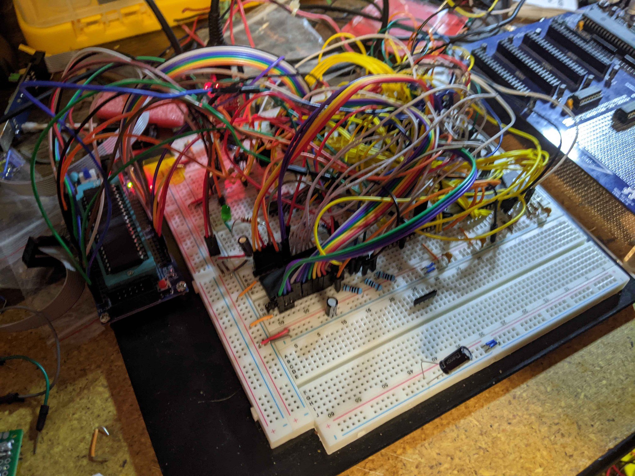
The boards are off to PCBWay, and in manufacture currently. While I wait I have the breadboard prototype to experiement with the firmware. I am hesitent to make any design changes to the nightmere of wires the breadboard has become:
![]()
In the meanwhile I want to thank you for taking the time to review my project. I have some schematics loaded into the files section at the top of the project page, and you can review the spreadsheet that outlines the memory map further. I think I made enough space in the memory map that level 1 of OS-9 compatibility should be feasable, though its a long way off if its even possible. The applications for having a uni-paripheral are almost endless, the AVR can interface modern serial protocalls like SPI and I2C as well as provide a buffered UART using the relitively simple 6850 UART protocal (think a 6850 but with a FIFO!). Its a long road ahead but an exciting one!
See you all in a week or two once the prototype is assembled!
HB63C09M - 10x10 HD63C09 Based SBC
This is my project page for my new home brew computer, a multi-processor 63c09 and AVR SBC.
 Dave Collins