Gangwa Labs
-
Reflow.Card Dev Log 6 6.30.24
06/30/2024 at 19:16 • 0 commentsAfter Uploading all the dev logs and Reflecting back on the progress on this project I have some thoughts about the entire process and how I've approached design and more importantly documentation.
1. Documentation: I really wish I was documenting this project live more often instead of just uploading straight from my own notes. A better method could've been still taking my Dev Logs in my notes because I believe it's very important to write down what I'm learning and have something to look back on but more importantly after I'm done working condensing what I've learned into a more understandable and logical dev summary would be nice to look back on.
2. Design process: I wish that I maintained a better Github for this project as it would be nice to look back on the progress that I've made and understand the design changes over time instead of just massive uploads at a time.
Issues! I realized as I was creating the Instructions for the project that I messed up big time! In order to power the Control MCU to the proper 3.3v it needs a 20v source as I've configured it with a 20v Buck Converter. HOWEVER! In order to program it through the USB-C port it needs to come from a computer which is not going to output the 20v power. The next iteration of this design should account for that discrepancy and should integrate a switch and an LDO to direct the power through the LDO if it's getting power through a computer and is being programmed and then if it's getting power from a 20v power source it should direct power through the buck converter. It will be interesting to see how I manage that problem. -
Reflow.Card Dev Log 5 6.21.24
06/30/2024 at 19:09 • 0 commentsThis Dev Log is pulled straight from my notes
Goals
- [x] complete Schematic ✅ 2024-06-24
- [x] Add all JLCPCB part numbers to components ✅ 2024-06-24Notes
- found new buck converter to step down 20v pd signal to power esp32
- Found inductor for buck converter (C2827354)
- Found Diode for buck converter SS54 (C22452)
- Recycled MOSFET from PD switch for Load switch for Heater -
Reflow.Card Dev Log 4 6.2.24
06/30/2024 at 19:08 • 0 commentsThis Dev log is pulled straight from my notes while working on the project
Goals
- understand how to read an NPN transistor datasheetReading NPN Transistor Data sheets
- VCE(sat): when the transistor is in saturation mode and is acting as a switch there is a measured drop in voltage from collector to emitter which is rated as VCE(sat)
- NPN transistors are current driven devices so the primary information and concern is current related
- Ic = Ib x hFE
- Icex = collector current cutoff: leakage current through the collector to emitter when the device is off
- hFE(includes leakeage) = hfe(small signal current gain)
- hFE(Current gain) varies with Ic(collector current)
- Vbe(on) = Base-Emitter on voltage: Voltage at which current begins to flow and the collector starts to draw current
- Saturation mode: using the transistor as a switch
- minimum voltage between the collector and the emitter is called Collector-Emitter Saturation voltage (Vce(sat)) often 0.2v to 0.3v
- Ic at maximum: the transistor can not put anymore current through it
- Vce at minimum: the voltage drop between collector and emitter is at a minimum
- The current at the collector is not responding to a change in the base current
- Power dissipation
- Pd = Ir x Vr
- power dissipated across a resistor is equal to the current through the resistor times the voltage across the resistor
- Pd(total) = Pd(C) + Pd(B)
- there is power being dissipated through both the base and the collector in a BJT
- Pd(actual) < 0.5 x Pd(datasheet)
- actual power dissipation must be half the rated value for safety rating
- Ic = Max Collector Current: maximum current that you should have running through the device
- Ic(actual) < (2/3) x Ic(datasheet)
- actual current should be 2/3 or less of rated value for safety rating
- Maximum Voltage rating for safety ratings
- V(actual) < (2/3) x V(datasheet)
- Past the saturation region is the active region where any increase in Ib doesn't increase Ic
- In the active region the Ic stays the same over a long Vce range
- IE. Past a certain voltage (Vce(sat)) the Transistor doesn't care what voltage is across Vce as the Ic stays the same for that Ib
- General rule of them is that base current should be 1/10 the collector currentUpdated Design
- Using A gate driver instead of a NPN for the MOSFET and using a dual Channel MOSFET IC
- PD chip that can manage up to 20V 5A -
Reflow.Card Dev Log 3 6.1.24
06/30/2024 at 19:07 • 0 commentsThis Dev Log is pulled straight from my notes
Goals
- understand how NPN and MOSFET fit together to create a cheap control signal for the higher power PCB hotplate
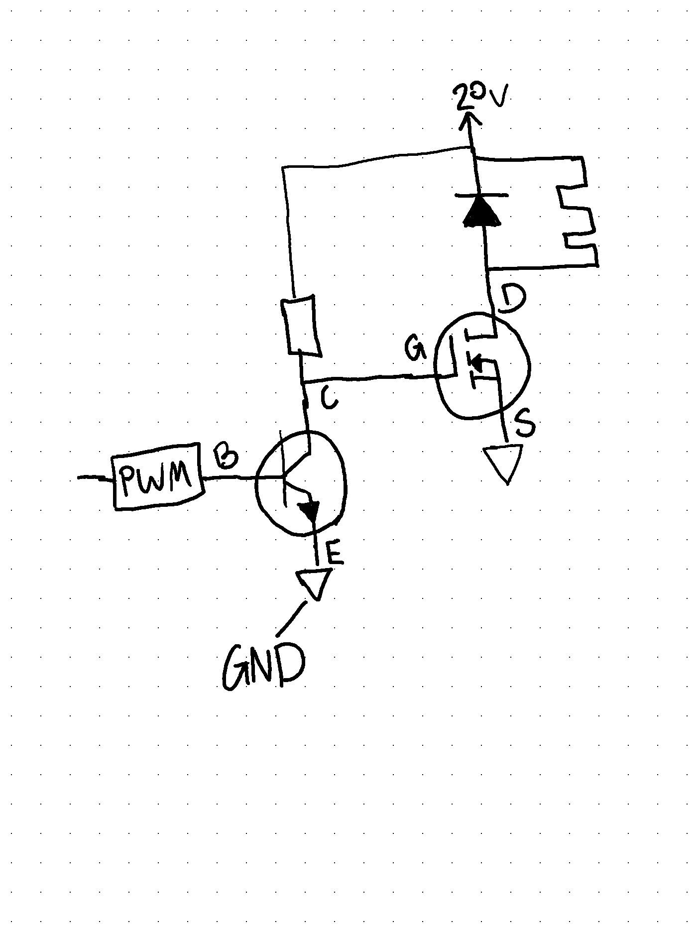
- Understand how the example Hotplate schematic worksSimplified Schematic
![]()
- NPN Transistor is acting as an inverting Switch ie. LOW from the PWM is 100% power
- When the NPN Transistor is turned on the Gate of the MOSFET is brought to ground via the collector-emitter path and this turns off the MOSFET
- When the transistor is off the voltage at the gate is higher than the Source(GND) and the current is free to flow through the resistive heater and from Source to Drain completing the circuitSourcing Components
MOSFET
- 20V VGS with more than 3A of Drain continuous CurrentBJT
- Collector to emitter voltage of 20V
- Collector Current able to withstand more than 3A for safety rating
- Base voltage at 3.3v micro-controller level and able to be controlled with 20mA or less of currentReading BJT Datasheets
- ?????? -
Reflow.Card Dev Log 2 5.30.24
06/30/2024 at 19:05 • 0 commentsThis Dev Log is pulled straight from my notes
Goals
- Understand the difference between N and P channel MOSFETs
- Understand NPN transistors
- finalize components needed in the circuitN channel vs P Channel Mosfet
- N-Channel MOSFET is triggered by applying a **Positive** voltage to the gate relative to the source
- Used when switching load side
- P-Channel MOSFET is triggered by applying a **Negative** voltage to the gate relative to the source
- Used when switching ground sideNPN Transistor
- type of BJT (Bipolar Junction Transistor)
- commonly used for amplification or switching
- Pins
- Collector
- Positive end of the transistor
- Connected to the high voltage potential or positive supply
- when transistor is turned on current flows from collector to emitter
- Usually connected to the load
- Base
- control terminal of the transistor
- current flowing into the base controls the current flow from collector to emitter
- Relationship between base and collector current is determined by the transistor gain (hFE)
- Emitter
- Negative terminal of the transistor
- connected to negative side or ground
- current flows from collector to emitter when transistor is turned on
- When enough positive voltage is applied to the base current flows from collector to emitter the amount of current that flows is proportional to the amount of current flowing into the base and is tied to the transistor gain.
- Collector-Emitter junction is normally **Reverse-biased** meaning that the collector voltage is higher than the emitter voltage. This acts as an open switch preventing current from flowing from collector to emitterDatasheet Values to Look for
- Collector-Emitter Voltage (VCEO): maximum voltage that can be applied between collector and emitter when the base is open
- Collector-Base Voltage (VCBO): Maximum voltage that can be applied between the collector and the base when the emitter is open
- Emitter-Base Voltage (VEBO): maximum voltage that can be applied between the emitter and the base when the collector is open
- Collector Current (IC): Maximum continuous Current that can flow through the transistor from collector to emitter
- Leakage Current (ICEO): Current that flows from Collector to emitter when the transistor is off
- Power Dissipation (PD): Max power the transistor can dissipate without damage
- Current Gain (hFE): ratio of collector current to base current
- How much can the transistor amplify current going into the base pin
- Transition Frequency (fT): Frequency that the transistor can switch on and off
- Collector-Emitter Saturation Voltage (VCE(sat)): the minimum voltage drop from collector and emitter when the transistor is properly saturated.
- Base-Emitter On-Voltage(VBE(on)): minimum voltage required between base and emitter to turn the transistor on
- Collector-Emitter Breakdown Voltage (BVCEO): Voltage at which the reverse-biased collector-emitter junction failsVoltage Divider
- Uses 2 Resistors to divide a larger voltage into a smaller one
- Used to created a reference voltage
- simple Schematic
Vin ---+
|
R1
|
Vout --+
|
R2
|
GND ---+
- the output voltage is determined by the ratio of the resistance of R1 and R2 according to the formula
- Vout = Vin x (R2/ (R1+R2))
- Vin is the input voltage
- Vout is the output voltage between the 2 resistors
- You can get any voltage between Vin and V0
- Limited when it comes to supplying current to a load
- Used only in high impedance loads or other circuits that draw minimal current
Reflow.Card
A 2 PCB USB-C PD powered reflow hotplate in the form factor of a business for on the go reflow soldering