agp.cooper
-
Optimisation
02/27/2017 at 11:26 • 0 commentsOptimisation
I have been considering what to do next with the software PLL. Do I go the simple low pass filter and move on or spend more time optimising. It is a question of time versus likely outcomes. I have a good result, is it worth trying to make it better?
The second problem is how to optimise this problem? I can see two approaches:
- More theoretical research - Someone else may have already solved this problem.
- Use numerical methods to search the parameter space (maybe I will get lucky).
But first what is the problem I am trying to solve?
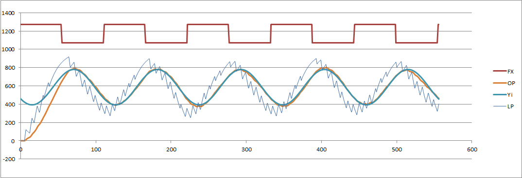
Here is a very good result from the Bell103A2 modem project:
![]()
What are the key attributes:
- a sine wave response with a period of 150 Hz
- centred around known mid point (zero in this case)
- the sine wave peaking at the end of the bit width pulse
- a smoothed square wave for longer pulse widths
- both the sine wave and smoothed square wave peaking at the maximum value
- the absence of noise at the peak values particularly for the smoothed square waves.
Here is a less than ideal response:
![]()
Back to phase locked loops
Here is my current low pass PLL response showing the data input (square wave), the LP output and a fitted sine wave:
![]()
So why is this important? Here is version that looked good in the beginning only to blow up latter:
![]() What when wrong?
What when wrong?Searching Parameter Space
What controls the output of the PLL? Yes I know about Q (transit overshoot) and natural frequency but the above image shows a stable PLL becoming unstable. To fix the above I increased the lower bound frequency to reduce the work for the PLL to get into lock.
What parameters can I play with?
- sample rate
- low frequency
- low pass filter frequency
Sample Rate
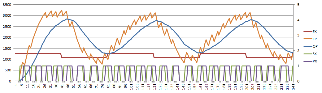
I am obviously very reluctant to change (increase) the sample rate. But here is the impact (SR = 8065):
![]()
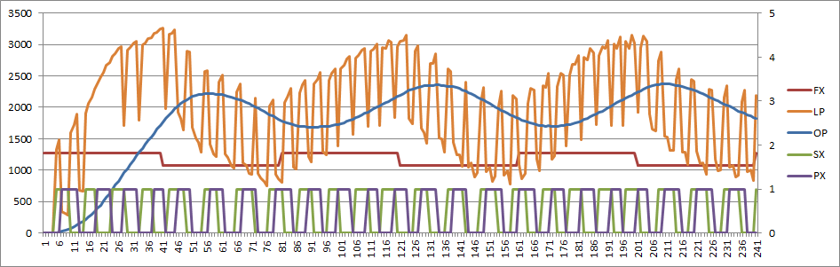
And (SR = 16667 Hz):
![]()
Note: the fitted sine wave (to the output) uses the last four cycles.
DDS Low Frequency
I already know this works but I don't know if the system is stable?
Low Pass Filter
Again, yes but the theory does not translate very well with a low sample rate.
What to do?
I am thinking that I could get really bogged down here. I have coded a steepest descent optimiser (but not run it ) but based on the rules of thumb that I already know I suspect I will not find anything new. The problem has multiple local optima (due to the discrete nature of a software PLL), so problem will not solve easily or reliable. I think I should move on!
Fitting a Sine Wave to the Data
I am familiar with multi-variate analysis so linearising and solving the equations is not too hard. The form of the equation I am trying to solve is:
- Y = A + B * Sin(2 * Pi * F * t + P)
where:
- B is the amplitude (to solve)
- F is the frequency (known, that is 150 Hz)
- P is the phase (to solve)
- A is the offset (known but will solve anyway)
Separate the Frequency and Phase using:
- A + B * Sin(2 * Pi * F * t + P)
- A + B * Cos(P) * Sin(2 * Pi * F * t) + B * Sin(P) * Cos(2 * Pi * F * t)
Therefore (after relabelling the constants):
- Y = A0 + A1 * Sin(2 * Pi * F * t ) + A2 * Sin(2 * Pi * F * t )
The error squared function is:
- E2 = (Y - (A0 + A1 * Sin(2 * Pi * F * t ) + A2 * Sin(2 * Pi * F * t ) ))^2
Solving the multi-variate problem:
- Sum(Y) = A0 * (N + Sum(Cos(2 * Pi * F * t)) + Sum(Cos(2 * Pi * F * t)))
- Sum(Y * Cos(2 * Pi * F * t)) = A1 * (Sum(Cos(2 * Pi * F * t)) + Sum(Cos(2 * Pi * F * t) * Cos(2 * Pi * F * t)) + Sum(Cos(2 * Pi * F * t) * Sin(2 * Pi * F * t)))
- Sum(Y * Sin(2 * Pi * F * t)) = A2 * (Sum(Sin(2 * Pi * F * t)) + Sum(Cos(2 * Pi * F * t) * Sin(2 * Pi * F * t)) + Sum(Sin(2 * Pi * F * t) * Sin(2 * Pi * F * t)))
Where N is the number of samples.
Fortunately the above simplifies if the range of "t" is a multiple of 2 * Pi, to:
- Sum(Y) = A0 * N
- Sum(Y * Cos(2 * Pi * F * t)) = A1 / 2 / N
- Sum(Y * Sin(2 * Pi * F * t)) = A2 / 2 / N
Therefore:
- A0 = Sum(Y) / N
- A1 = 2 * Sum(Y * Cos(2 * Pi * F * t)) / N
- A2 = 2 * Sum(Y * Sin(2 * Pi * F * t)) / N
Here it is in VBA code:
A0 = 0
A1 = 0
A2 = 0
For Time = Int(SR / 150 + 0.5) To Int(5 * SR / 150 + 0.5)
  A0 = A0 + Test(Time)
  A1 = A1 + Test(Time) * Cos(2 * Pi * Time * 150 / SR)
  A2 = A2 + Test(Time) * Sin(2 * Pi * Time * 150 / SR)
Next Time

A0 = A0 / Int(4 * SR / 150 + 0.5)
A1 = 2 * A1 / Int(4 * SR / 150 + 0.5)
A2 = 2 * A2 / Int(4 * SR / 150 + 0.5)
E2 = 0
For Time = 0 To Int(5 * SR / 150 + 0.5)
  ActiveSheet.Cells(Time + 3, 8).Value = Space - 20
  ActiveSheet.Cells(Time + 3, 9).Value = A0 + A1 * Cos(2 * Pi * Time * 150 / SR) + A2 * Sin(2 * Pi * Time * 150 / SR)
  If (Time >= Int(SR / 150 + 0.5)) Then
    E2 = E2 + (Test(Time) - (A0 + A1 * Cos(2 * Pi * Time * 150 / SR) + A2 * Sin(2 * Pi * Time * 150 / SR))) ^ 2
  End If
Next Time
Back to the Modem Problem
Yes a PLL will work (quite well).
The other problem was removing jitter by extracting the clock. Well I have not really looked at that but I can now extract a fitted sine wave (with limitations) that could resolve much of the jitter. The error would be low on the transition and the fitted sine wave used to determine zero crossing. The computation effort though is not likely to work with the limited computational bandwidth of the Arduino CPU.
Regards AlanX
-
Porting to the Arduino
02/20/2017 at 03:21 • 0 commentsFSK Modem
The purpose of this project was to see if I could improve the performance of my Bell 103A2 modem. Initially to see if I could extract the baud clock to mitigate output jitter. Well I have not looked at that (have to investigate other start bit synchronisation methods as well), the FSK Modem is a good platform to test the PLL as most of the code has been written (and debugged) and it has a built in loop-back test.
All I need to do is replace the demodulation code subject to a decision on (1) a binary XOR or (2) a mixer style phase detector.
An unreasonable good results should be expected from the loop-back as the baud generator is not really asynchronous. Well this has to be tested.
The First Port
For the first port I dropped the sample frequency to 8065 Hz to match the FSK modem. I tested bothe the Anwer and Originate mark/space frequencies. This uncovered a problem for the PID version of the PLL. Although adjustment of the parameters found an acceptable performance solution, the simple low pass PLL worked better. It appears that damping factor and natural frequency are not that important performance controls!
The Second Port
The second port is based on the low pass PLL and an internal loop back test. I am on holidays so no test work, but here is the code:
//  Bell 103A2 Modem
//  ================

#define ModemMode false // Answer Modem -> Receives Low Channel
#define Baud        300 // Baud rate
#define TimerConst   30 // 8065 Hz sample rate
// Phase steps based on PWM frequency of 31372.5 Hz (=16000000/510)
#define BaudPhase   627 // Baud phase increment (for 31372.5 Hz clock)
#define OriFspace  2235 // Originate modem Space frequency 1070 Hz
#define OriFmark   2653 // Originate modem Mark  frequency 1270 Hz
#define AnsFspace  4230 // Answer modem    Space frequency 2025 Hz
#define AnsFmark   4648 // Answer modem    Mark  frequency 2225 Hz
#define AnsPM      7882 // Answer modem tuning word for 970 Hz
#define OriPM     15643 // Originate modem tuning word Fore 1925 Hz

// Constants
const unsigned int SR=12000;        // Sample Rate
const unsigned int PL=870;          // Originate PLL Low Frequency
const unsigned int PH=1825;         // Answer PLL Low Frequency
const unsigned int PML=PL*65536/SR; // Originater DDS Tunning Number
const unsigned int PMH=PH*65536/SR; // Answer DDS Tunning Number


// Define various ADC prescaler
const byte PS_16=(1<<ADPS2);
const byte PS_32=(1<<ADPS2)|(1<<ADPS0);
const byte PS_64=(1<<ADPS2)|(1<<ADPS1);
const byte PS_128=(1<<ADPS2)|(1<<ADPS1)|(1<<ADPS0);

// A 64 step byte sized sine table
const byte iSin[64] = {
  128,140,153,165,177,188,199,209,
  218,226,234,240,245,250,253,254,
  255,254,253,250,245,240,234,226,
  218,209,199,188,177,165,153,140,
  128,116,103, 91, 79, 68, 57, 47,
   38, 30, 22, 16, 11,  6,  3,  2,
    1,  2,  3,  6, 11, 16, 22, 30,
   38, 47, 57, 68, 79, 91,103,116
};

// Debug variables
// volatile int I=0;
// volatile int D0[324];
// volatile int D1[324];

// Get a signal sample
volatile bool dataAvailable=false;
volatile int SX0=0;
volatile int SX1=0;
volatile int SX2=0;
ISR(TIMER0_COMPA_vect) {
  // Roll the samples
  SX2=SX1;SX1=SX0;
  // SX0=analogRead(A0)-512;
  SX0=OCR2A-128;
  // Flag new sample available
  dataAvailable=true;
}

// TRANSMIT
volatile byte DataOut=1;
volatile bool baudUpdate=true;
volatile unsigned int baudTick=0;
ISR(TIMER2_OVF_vect) {
  static unsigned int phase=0;
  OCR2A = iSin[(phase>>10)]; // Output on pin 11
  if (!ModemMode) {          // Set true for Answer modem - Invert for audio loopback test
    // Answer modem
    if (DataOut==0) {
      phase+=AnsFspace;
    } else {
      phase+=AnsFmark;
    }
  } else {
    // Originate modem
    if (DataOut==0) {
      phase+=OriFspace;
    } else {
      phase+=OriFmark;
    }
  }
  // Update baud tick
  baudTick+=BaudPhase;
  if (baudTick<BaudPhase) baudUpdate=true;
}

void setup() {
  pinMode(A0,INPUT);                               // Audio input
  pinMode(12,OUTPUT);                              // Digital data output
  pinMode(11,OUTPUT);                              // Audio output (PWM)
  pinMode(10,OUTPUT);                              // Digital data input
  pinMode(LED_BUILTIN,OUTPUT);                     // Signal detected
  digitalWrite(LED_BUILTIN,LOW);

  // Set ADC prescaler (assume a 16 MHz clock)
  ADCSRA&=~PS_128;                                 // Remove bits set by Arduino library
  ADCSRA|=PS_16;                                   // 16 prescaler (1 MHz)

  // Disable interrupts
  cli();

  // Use Timer 0 for sample rate (8065 Hz)
  // ATmega48A/PA/88A/PA/168A/PA/328/P
  TIMSK0 = 0;                                      // Timer interrupts off
  TCCR0A = (2 << WGM00);                           // CTC mode
  TCCR0B = (3 << CS00);                            // prescaler 64, 16 MHz clock
  TIMSK0 = (1 << OCIE0A);                          // COMPA interrupt
  OCR0A = TimerConst;                              // Sample rate: 8065 Hz = 250 kHz / (30+1)

  // Use Timer 2 for Audio PWM
  // ATmega48A/PA/88A/PA/168A/PA/328/P
  TIMSK2 = 0;                                      // Timer interrupts off
  TCCR2A = (2 << COM2A0)|(1 << WGM20);             // Phase correct PWM (31.25 kHz), toggle output on OC2A (PB3/D11)
  TCCR2B = (0 << WGM22)|(1 << CS20);               // 16 MHz clock (no pre-scaler)
  OCR2A = 128;                                     // Set 50% duty
  TIMSK2 = (1<<TOIE2);                             // Set interrupt on overflow (=BOTTOM)

  // Enable interrupts
  sei();
}


int Demodulate(bool Mode) {
  static unsigned int K=3000; // PLL Gain
  static unsigned int SX=0;   // Signal
  static unsigned int PX=0;   // PLL Frequency
  static unsigned int PA=0;   // PLL Phase Accumulator
  static unsigned int PM=0;   // PLL Phase Increment
  static unsigned int PD=0;   // PLL Phase Detector
  static unsigned int LP=0;   // VCO Control
  static unsigned int OP=0;   // Output filter
  // Bandpass filter
  static unsigned int BA0=0;
  static unsigned int BA1=0;
  static unsigned int BA2=0;
  static unsigned int BB0=0;
  static unsigned int BB1=0;
  static unsigned int BB2=0;
  static unsigned int BP0=0;
  static unsigned int BP1=0;
  static unsigned int BP2=0;

  // SIGNAL DECODER
  BA2=BA1;BA1=BA0;
  BB2=BB1;BB1=BB0;
  BP2=BP1;BP1=BP0;
  if (Mode) {                         // Set true for Answer modem
    // PLL DDS TUNING NUMBER
    PM=AnsPM;
    // ANWSER MODEM BANDPASS FILTER (Fc = 1170 Hz)
    BA0=(8*(SX0-SX2)+7*BA1-4*BA2)>>3;
    BB0=(3*(BA0-BA2)+7*BB1-4*BB2)>>3;
    BP0=(2*(BB0-BB2)+7*BP1-4*BP2)>>3;
  } else {
    // PLL DDS TUNING NUMBER
    PM=OriPM;
    // ORIGINATE MODEM
    BA0=(8*(SX0-SX2)-BA1-4*BA2)>>3;   // Bandpass (Fc = 2125 Hz)
    BB0=(3*(BA0-BA2)-BB1-4*BB2)>>3;
    BP0=(2*(BB0-BB2)-BP1-4*BP2)>>3;
  }

  // BINARY SIGNAL
  SX=(BP0>=0)?1:0;

  // PLL VC0
  PA=PA+PM+LP;
  PX=PA>>15;

  // XOR PHASE DETECTOR
  PD=(SX==PX)?PD=0:PD=K;

  // LOOP FILTER
  LP=PD+7*(LP-PD)>>3;

  // OUTPUT FILTER
  OP=OP+7*(OP-LP)>>3;

  // Debug: Record data for post analysis
  // if (I<324) {
  //    D0[I]=SX0;
  //    D1[I]=BP0;
  //    I++;
  // }

  // Return correlation flag
  if (OP>=0) {
    return(1);
  } else {
    return(0);
  }
}

void loop() {
  static bool Mode=ModemMode;
  static byte DataIn=1;
  static byte i=0;

  // SEND DATA
  if (baudUpdate) { // Counter has overflowed
    i++;
    if (i==1) DataOut=1;
    if (i==2) DataOut=0;
    if (i==3) DataOut=1;
    if (i==4) DataOut=1;
    if (i==5) DataOut=0;
    if (i==6) DataOut=0;
    if (i==7) DataOut=1;
    if (i==8) DataOut=1;
    if (i==9) DataOut=1;
    if (i==10) DataOut=0;
    if (i==11) DataOut=0;
    if (i==12) DataOut=0;
    if (i>=12) i=0;
    baudUpdate=false;
    // digitalWrite(10,DataOut);
  }

  // RECEIVE DATA
  if (dataAvailable) {
    // Demodulate signal and set D12
    DataIn=Demodulate(Mode);
    digitalWrite(12,DataIn);
    // Done, wait for next sample tick
    dataAvailable=false;
  }

  // Debug output
  // if (I>=324) {
  //   cli();
  //   Serial.begin(9600);
  //   for (I=0;I<324;I++) {
  //     Serial.print(I);
  //     Serial.print(",");
  //     Serial.print(D0[I]);
  //     Serial.print(",");
  //     Serial.println(D1[I]);
  //   }
  //   Serial.flush();
  //   Serial.end();
  //   while (true);
  // }

}
TBC ...
AlanX
-
Loop Filter Shoot Off
02/20/2017 at 01:47 • 0 commentsLoop Filters
I have been working my way through the loop filter types, so far:
- Low Pass
- 1st order PID
- Passive Lead-Lag
- Active Lead-Lag
No problem with the first three:
Low Pass
![]()
PID
![]()
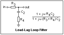
Lead-Lag
![]()
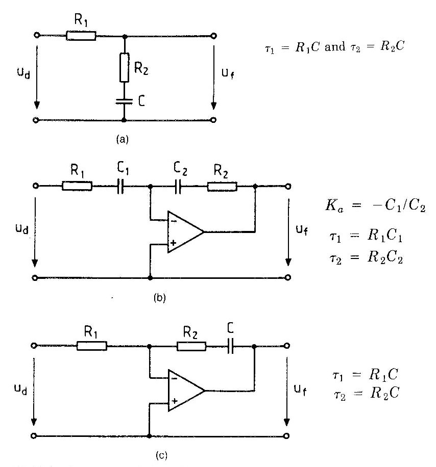
The Active Lead Lag Filter
Here are the analog domain basic loop filters. The problem filter is shown at the bottom of the image:
![]()
(source: http://www.globalspec.com/reference/38390/203279/2-6-second-order-phase-locked-loops)
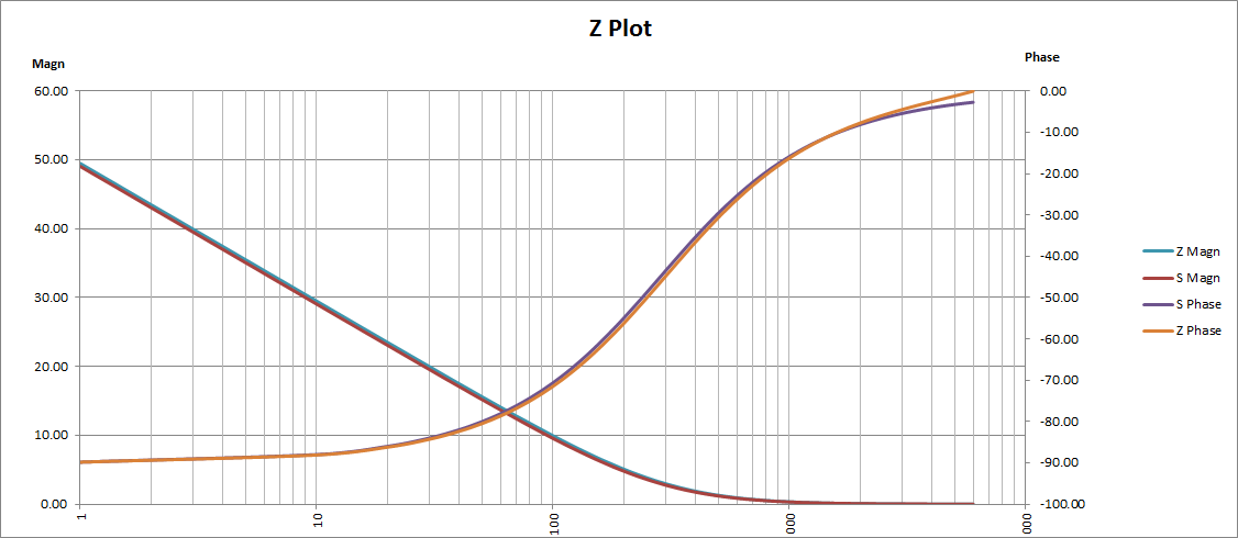
I have plotted the S domain versus the the modelled Z domain and the Z domain is good up until about Nyquist, so no problems:
The recursive equation was:![]()
- LP0 = (69 * PD0 + 10 * PD1 - 59 * PD2 - 0 * LP1 + 64 * LP2) \ 64
The issue is that this filter cannot be used directly. The DC gain is +46dB and as the structure is that of an integrator and the PD is 0 to K, the filter just blows up:
This can be fixed by using a differential PD (i.e. -K/2 to +K/2) or by using a filter like the second filter below:![]()
![]()
After substituting the PD for a differential PD (i.e. -K/2 to +K/2) I get something that basically works:
![]()
(Note that the vertical scale has changed compared to the other PLL filters)
The analog equivalent is:K 4000 =KpKv R1 5600 R R2 5600 R C 0.000000100 F T1 0.00056 T2 0.00056 WN 2673 =sqrt(K/T1) D 0.75 =T2/2*sqrt(K/T1) The main advantage of the last filter is greater range of control of damping factor and natural frequency.
Choosing a Loop Filter (The Shoot Off)
Now that I have all the filters working which one to use going forward? Active Lead-Lag or PID?
Active Lead-Lag Loop
Inputs:
- K (KpKv)
- R1
- R2
- C
Intermediate:
- T1 (=R1C)
- T2 (=R2C)
- WN (=sqrt(K/T1))
- D (=T2/2*sqrt(K/T1))
Code (after calculating Z-transform coefficients):
- PD2 = PD1
- PD1 = PD0
- PD0 = PD * K - K \ 2
- LP2 = LP1
- LP1 = LP0
- LP0 = (B0 * PD0 + B1 * PD1 + B2 * PD2 - A1 * LP1 - A2 * LP2) \ D
- LP = LP0
PID Loop (First Order)
Inputs:
- WN (natural frequency)
- D (damping factor)
- SR (sample rate)
Intermediate:
- T1 = 1 / WN / WN
- T2 = 2 * D / WN
Output:
- Kp = Proportional factor
- Kp = (1 + 1 / Tan(1 / (2 * T2 * SR))) / (2 * T1 * SR)
- Kp ~ (1 + 2 * T2 * SR) / (2 * T1 * SR)
- Ki = Integral factor
- Ki = 1 / (T1 * SR)
Code:
- PD1 = PD0
- PD0 = PD
- LP = Kp * PD0 + (Ki + Kp) * PD1 - LP
Conclusion (The Shoot Off Results)
It looks rather like a "no-brainer" to go with PID from a computational point of view (all other things appearing to be equal). Funny how the common wisdom of PID in the discrete domain is confirmed!
AlanX
-
The Low Pass Filter
02/16/2017 at 08:45 • 0 commentsWhat a can of worms!
The mixing of analog and digital can get very messy. I spent the day transposing the lead-lag low pass filter into digital via the z-transform. I think the coefficients model the filter but how to be sure? The coefficients however are not that integer friendly.
The Wiki PLL uses a "Proportional and Derivative" concept that basically equates to a variable gain one pole low pass.
The Wiki PLL page discusses the problem with a simple RC filter, that independent control of damping factor and natural (i.e. damping) frequency is not possible:
- wn = ((KpKv)/(RC))^0.5
- d = ((KpKv)*(RC))^-0.5
For critical damping (d=0.7071):
- RC = 1/(2*KpKv)
Therefore (the low pass corner frequency) should be:
- wc = 1.414*KpKv !!!
The reason for pursuing the lead-lag filter is that the low pass corner frequency and the damping factor can be separated:
- wc = (R1+R2)*C
- wn = ((KpKv)*wc)^0.5
- d = wn*(R2*C+1/(KpKv))/2
- = wn*R2*C as 1/(KpKv) is small.
Neat.
What is not said is that we can easily change the K (i.e. KpKv) of the PLL. This is what I did to get rid of the overshoot. We still need a minimum K to ensure capture and lock of the signal.
The digital maths here is much like a Proportional-Integral-Derivative (PID) control. So more research required.
The 565 PLL FSK Modem
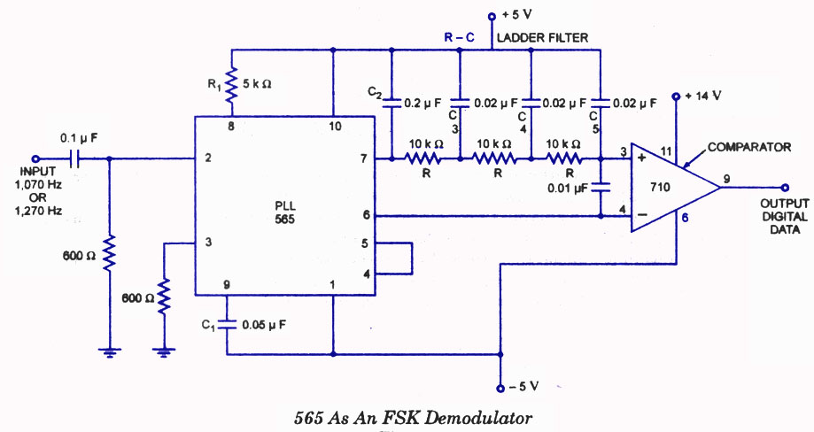
I was looking for some example FSK PLL circuits to analysis (surprising few with component values). I have seen this image many times:
![]()
Checking the datasheet:- Fo = 1170 Hz
- Fl = +/-936 Hz
- KpKv = 3931
For a simple RC LPF:
- Fc = 885 Hz
- Fn = 744 Hz
- d = 0.59
It is clear the designer wanted near critical damping and had no choice but the accept the LPF corner frequency of 885 Hz. In order to compensate the designer used a three stage low pass filter on the demodulated output.
Why did the designer not use a lead-lag filter:
- R1:
- Rinternal 3k6
- Rextrernal 2k2
- R2 15k
- C 0.05uF (no change)
- Fc = 153 Hz (good for 300 baud)
- Fn = 309 Hz
- d = 0.73
I have noticed that others (more recent) have used a low pass capacitor of 0.15 uF which results in:
- Fc = 295Hz (good for 300 baud)
- Fn = 429 Hz
- d = 0.34
Although the low pass filter is better the damping is probably too low.
Designing the Loop Response
Analog Domain
In the analog domain the process seems to be:
- select a damping factor (d) between 0.5 and 1.0 (minimise overshoot)
- select the minimum natural frequency (wn) that meets:
- lock time ~2*pi/wn
- lock/capture range ~2*d*wn
- use lead-lag filters to customise d and wn
I did not have success using a two stage single pole low pass filters.
Digital Domain
In the digital domain the "filter" of choice is PID (Proportional, Integral and Derivative), actually just Proportional and Integral. Here we select wn and d and determine Kp and Ki (the factor for proportional and integral):
- T1 = 1 / WN / WN
- T2 = 2 * D / WN
- B0 = (1 + 1 / Tan(1 / (2 * T2 * SR))) / (2 * T1 * SR)
- B1 = (1 - 1 / Tan(1 / (2 * T2 * SR))) / (2 * T1 * SR)
- Kp = B0
- Ki = B0 + B1
Where:
- WN is the natural frequency
- D is the damping factor
- SR is the sample rate
- T0, T1, B0 and B1 are temporary variable
A first order discrete equation is:
- PD1 = PD0
- PD0 = PD
- LP = Kp * PD0 + (Ki + Kp) * PD1 - LP
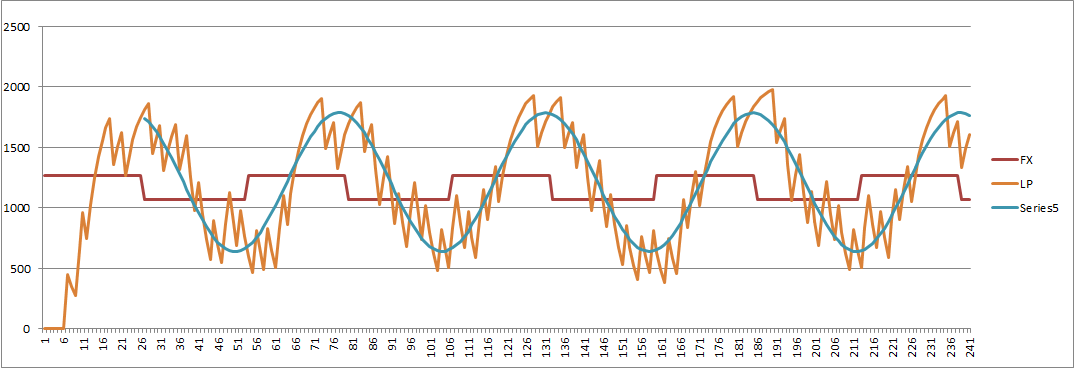
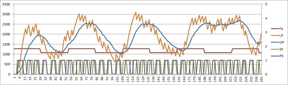
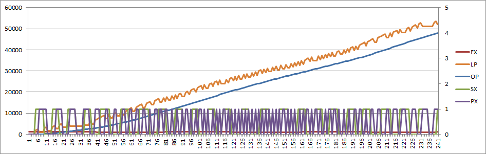
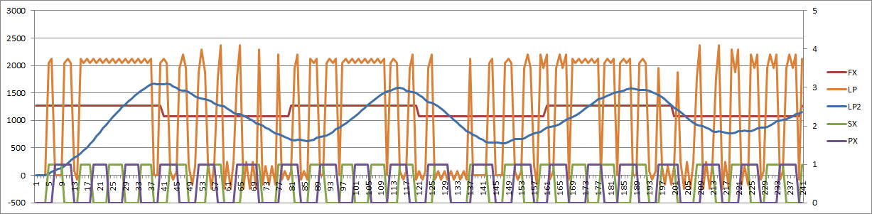
Results
Both work but the sinple low pass filter worked better in my case.
Here is the simple LP filter version:
![]()
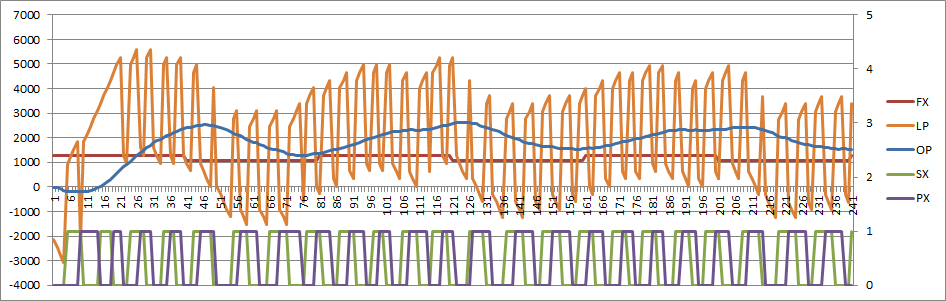
And here is the PID version:
![]()
The PID output is the orange (LP) curve. Not sure that the PID control signal should swing from limit to limit.
Plotting S Domain and Z Domain Functions
I have not looked at Laplace equations for 30 years and I am not an electrical/electonics engineer so it was a bit of "going back to school". Anyway, worked it out:
- Magn = |F(s)|
- Phase = arctan(Imaginary/Real)
I also worked out how to do the Z domain thanks to:
I have also worked out how to build discrete active filters thanks to:
Why it took a week or more to find this webpage I do not understand!
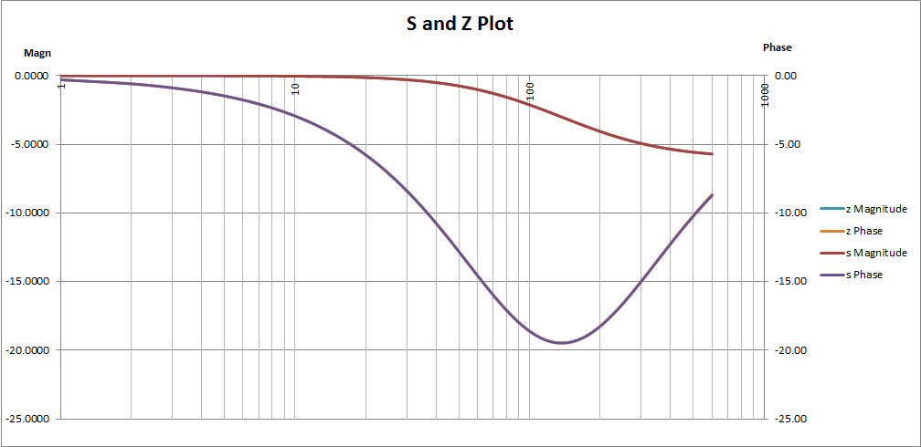
Here is an s and z domain plot for a simple lead-lag filter (in this case R1=8k2, R2=8k2 and C=50nF):
Note: there are only two curves because the s and z domains match.![]()
So I have all the tolls I need for a digital PLL.
AlanX
-
Building a Software PLL
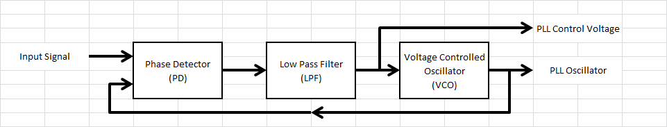
02/15/2017 at 01:05 • 0 commentsBasic Components of a PLL
The basic components of a PLL are:
- Phase Detector
- Low Pass Filter
- Voltage Controlled Oscillator
Optionally:
- Divide by N Counter
- Output Low Pass Filter
Here is my basic PLL diagram:
![]()
The Phase Detector
There are a number of different types of phase detectors (PD). The most common are:
- XOR
- Edge detector
- Multiplier
I am only looking at the XOR (exclusive OR) detector here. If you are not aware, the XOR is a logic gate (i.e. 7486):
![]() This can be modelled as:
This can be modelled as:if (A==B) { PD=0; } else { PD=1; }Or more compactly as:
PD=(A==B)?0:1;A PLL needs some DC loop gain (usually refer to as Kpd*Kvco). For this PLL all the loop gain (PK) is provided by the PD (phase detector). The main reason id that an integer maths digital low pass works best with higher values (i.e 0 and 1 will not cut it).
So here is the final PD:
PD=(A==B)?0:PK;The Low Pass Filter
Here is a simple RC low pass (LP) filter:
![]() (source: www.learningaboutelectronics.com/images/Low-pass-filter-diagram.png)
(source: www.learningaboutelectronics.com/images/Low-pass-filter-diagram.png)A simple RC low pass has a corner frequency (Fc) of:
- Fc = 1/(2*Pi*R*C)
This can modelled as:
- LP = a*LP+(1-a)*PD
(You may recognise this as the exponential smoothing equation)
Where:
- a = Exp(-2*Pi*Fc/Fs)
Where Fs is the sample frequency (Fs).
This can be reworked as:
LP=LP+A*(PD-LP)/DWhere a = A/D, where A is an integer and D is a power of 2 (i.e. 2, 4, 8, ...).
The reason for D being a power of 2 is that division is expensive for the Arduino and arithmetic shift right (>>) is not.
Although the RC LP filter works the voltage response and can oscillate and a "Lead-Lag" filter is usually preferred as it has a faster response with less overshoot:
![]()
(source: mysite.du.edu/~etuttle/electron/circ116.gif)
I have yet to "digitised" the Lead-Lag loop filter (TBC ...).
The Digital Oscillators
The generation of a both the test signal (SX) and the PLL oscillator (PX) are based on the Direct Digital Synthesis (DDS) . I will uses a 16 bit phase accumulator both the signal and PLL accumulators (SA and PA). The tuning words (SM ans PM) are:
- SM = SF*2^16/Fs, where SF is the signal frequency
- PM = PL*2^16/Fs, where PL is the low PLL oscillator frequency
The DDS's are:
- SA=SA+SM
- PA=PA+PM
Note: that overflow does nor cause and error.
And to get the binary output frequency:
- SX=SA<<15;
- PX=PA<<15;
To increase the PLL oscillator frequency we add the LP output to the phase accumulator:
- PA=PA+PM+LP
So what have we done? The PLL VCO low frequency is set by PM and the high frequency by is set by PM+LP, as the LP values range from 0 to PK.
The maximum PLL VCO frequency (PH) is then:
- PH=PL+PK*FS/2^16
So magic, we can estimate PK from the difference between the required VCO high and low frequencies.
The two equations above code as:
SA=SA+SM;
PA=PA+PM+LP;
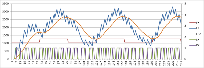
Here is the code written in Excel VBA:Option Explicit Sub PPL() Application.ScreenUpdating = False Application.Calculation = xlCalculationManual Application.EnableEvents = False Dim Pi As Double Pi = 4 * Atn(1) Dim FS As Long ' Sample Frequency Dim SX As Long ' Sample Input Dim SF As Long ' Sample Frequency Frequency Dim SA As Long ' Sample Frequency Phase Accumulator Dim SM As Long ' Sample Frequency Phase Increment Dim PX As Long ' PLL Frequency Dim PL As Long ' PLL Low Frequency Dim PM As Long ' PLL Phase Increment Dim PA As Long ' PLL Phase Accumulator Dim PD As Long ' PLL Phase Detector Dim PK As Long ' PLL Phase Detector Gain Dim LP As Long ' Low Pass Filter Dim LPF As Long ' Low Pass Filter Corner Frequency Dim LP2 As Long ' Output Low Pass Filter Dim A As Long ' Low Pass Filter Constant Dim D As Long ' Low Pass Filter Divisor Dim Time As Long ' Time Step FS = 12000 SF = 1070 SM = SF * 65536 \ FS SA = 0 SX = 0 PL = 800 PM = PL * 65536 \ FS PA = 0 PX = 0 PK = 5000 PD = 0 LP = 0 PK = Int(ActiveSheet.Cells(1, 10).Value + 0.5) LPF = Int(ActiveSheet.Cells(2, 10).Value + 0.5) D = 128 A = Int(D * Exp(-2 * Pi * LPF / FS) + 0.5) ActiveSheet.Cells(1, 1).Value = "Time" ActiveSheet.Cells(1, 2).Value = "FX" ActiveSheet.Cells(1, 3).Value = "SX" ActiveSheet.Cells(1, 4).Value = "PX" ActiveSheet.Cells(1, 5).Value = "PD" ActiveSheet.Cells(1, 6).Value = "LP" ActiveSheet.Cells(1, 7).Value = "LP2" For Time = 0 To 240 ' Sample Frequency (300 baud binary pattern) If (Time Mod 80 = 0) Then SF = 1070 SM = SF * 65536 \ FS End If If (Time Mod 80 = 40) Then SF = 1270 SM = SF * 65536 \ FS End If SA = SA + SM If (SA >= 65536) Then SA = SA - 65536 SX = SA \ 32768 ' PLL FREQUENCY PA = PA + PM + LP If (PA >= 65536) Then PA = PA - 65536 PX = PA \ 32768 ' XOR PD If (SX = PX) Then PD = 0 Else PD = PK End If ' PLL LPF (Fc = 100 Hz) LP = PD + A * (LP - PD) \ D ' Output FIlter LP2 = LP + A * (LP2 - LP) \ D ' Plot results ActiveSheet.Cells(Time + 2, 1).Value = Time ActiveSheet.Cells(Time + 2, 2).Value = SF ActiveSheet.Cells(Time + 2, 3).Value = SX ActiveSheet.Cells(Time + 2, 4).Value = PX ActiveSheet.Cells(Time + 2, 5).Value = PD \ PK ActiveSheet.Cells(Time + 2, 6).Value = LP ActiveSheet.Cells(Time + 2, 7).Value = LP2 Next Time Application.ScreenUpdating = True Application.Calculation = xlCalculationAutomatic Application.EnableEvents = True End SubHere is a plot with PK=5000:![]()
I have to say it does a pretty good job decoding the a FSK signal. A Lead-Lag filter should fix the initial over-shoot and speed up the response.
The mid point for the output signal (LP2) should be:
- LP = (1170-800)*65536/1200
- = 2021
Which matches the plot.
AlanX
Software Phase Locked Loop
The 567 tone decoder is perhaps most famous Phase Locked Loop (PLL) chip. This project looks at an Arduino software PLL.


 What when wrong?
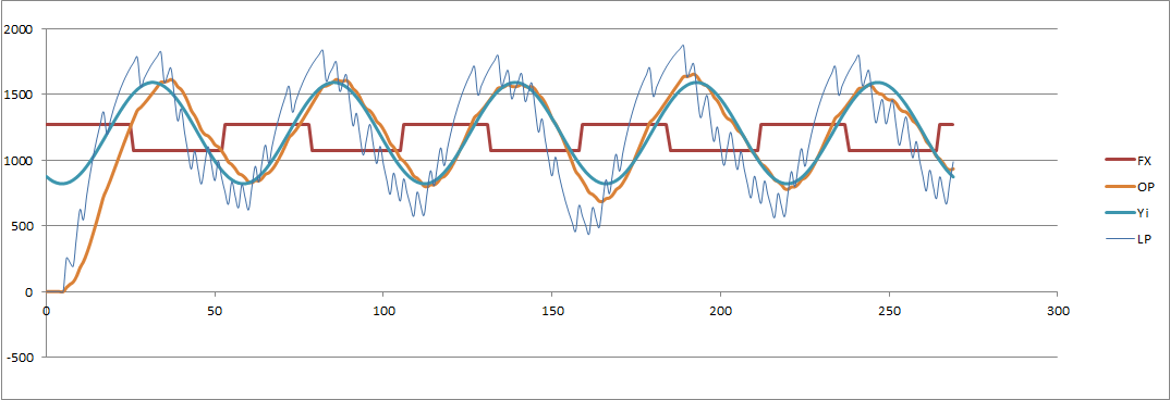


 This can be modelled as:
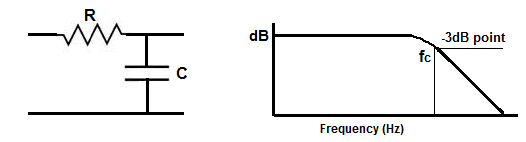 (source: