Eric Lind
-
Building stage 2 board - a slight hickup
12/14/2024 at 14:36 • 0 commentsSo after my son finally soldered the stage 2 board I started testing it, like checking all power connections, all grounds and generally check for shorts. And of course I found out that I had made a big mistake!
![]()
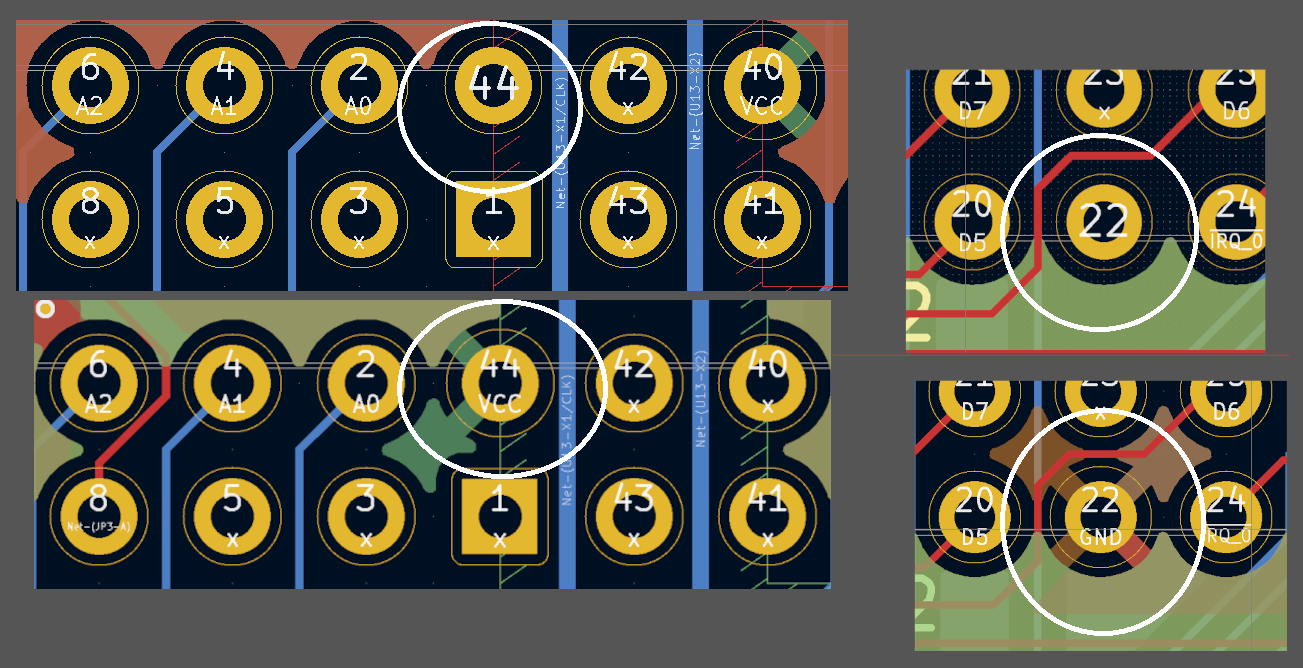
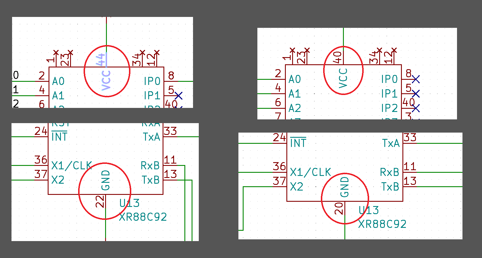
The power pin and ground pin on the serial controller is connected to wrong pins. And if you look in the schematics you can see that I made the symbol for it wrong.
![]()
Fortunately can it be "re-wired" to work. I will just bridge pin 44 to VCC, pin 40 is an unused input pin so it does not matter. And the ground had not been filled on pin 20 so that will not be a problem to just bridge pin 22 to GND.
Crisis adverted!
I will continue to check connections before i populate the board and power it up. I have measured the voltage from the regulator and it is nicely holding on 5.0v. Soon it is Christmas Hollydays and I will be able to take more time to test this bord.
-
Sometimes life comes in between
12/03/2024 at 09:56 • 0 commentsSadly I haven't soldered the stage 2 board yet, I've had birthdays and other family celebration preparations to tend to. But I still got time to do a visual inspection and found a couple of things that need fixing to stage 3. But none of them was a showstopper yet!
So what have I found so far:
- I'm missing an chip name on U26 a GAL chip. Definitely not a deal-breaker!
- Footprint on power switch SW1 is not correct (I made this my self and must have been holding my caliper upside down when i did it)
The hold pins (pins that are not connected but just a part of the switch chassis) are to close to the other pins.
The hole diameter is to small, the pins on the switch are quite large. - The USB socket is too far in to the board, it will not reach out of the case correctly.
- The same goes to the power socket, but I'm looking for another type of socket for that.
But none of these are bad enough to stop me from making a stage 2 machine to test on.
When I finalized the basic tests and those are ok, I'm curious if any one else is interested in trying this computer? I will probably have 2 or 3 boards over after the I've made my prototypes. And I think I will be able to send them out if any one is interested in this project. The only thing I ask of is to get feedback and hope that you will share what you have been doing on it with the "community" (thats what I call my self for now).
![]()
-
Stage 2 has arrived!
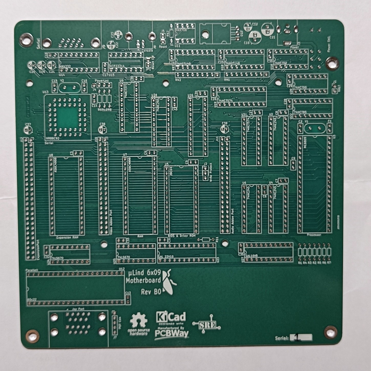
11/26/2024 at 19:36 • 0 commentsToday I surprisingly received the stage 2 boards! They where supposed to arrive tomorrow! But I'm not sad! They look amazing!
Huge thanks to PCBWay who reached out to me and wanted to support this project. They made a great job with these boards and the service was amazingly fast. As the buffoon I am I mistakingly chose wrong on some options when I ordered, but the sent me an question in just an hour to verify my choices. And all was cleared and the bords sent to production almost immediately.
![]()
Now we will begin to assemble a board an hopefully we will be able to do tests this weekend!
-
Stage 2 - On the way, the PCBWay!
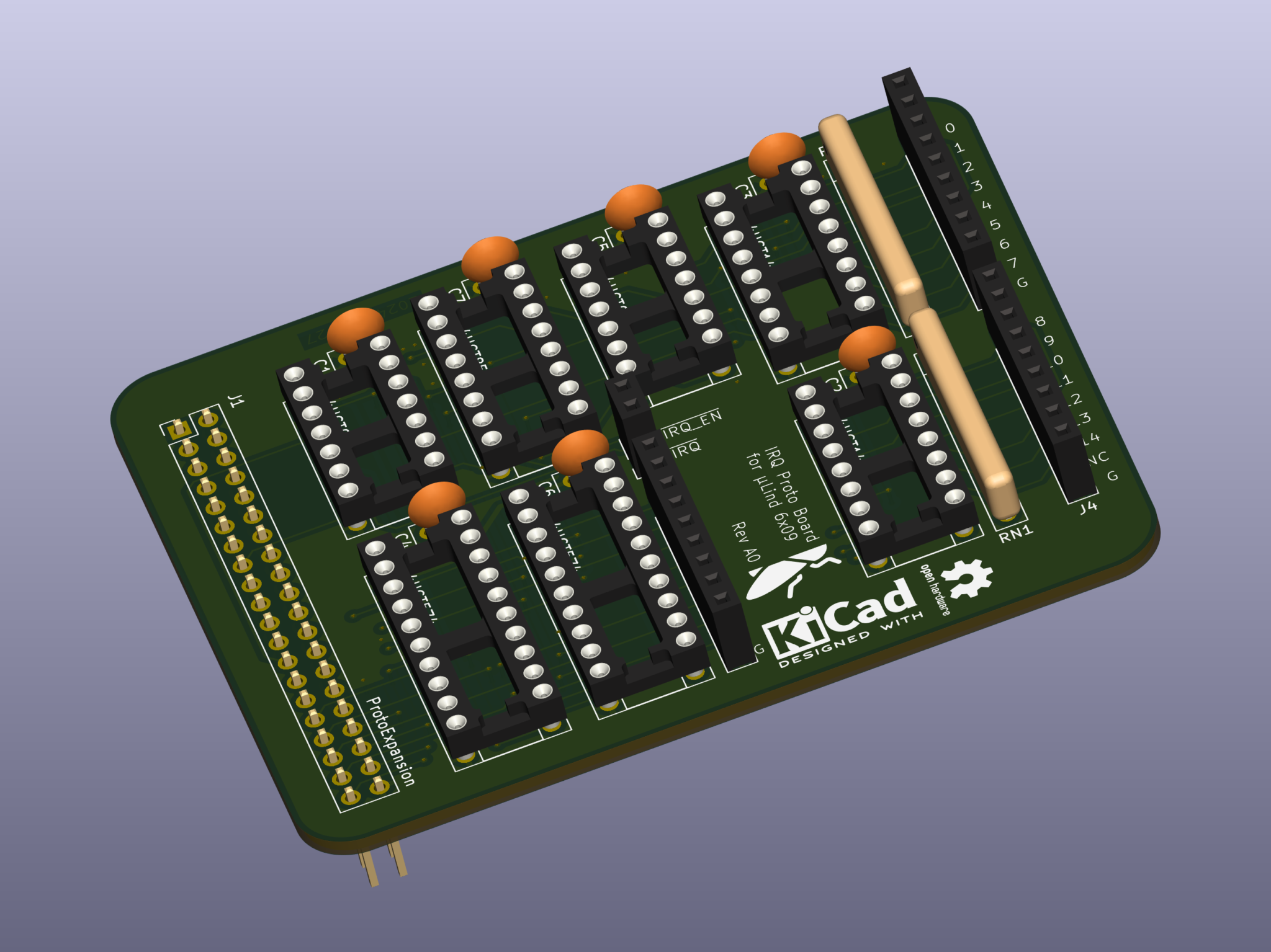
11/17/2024 at 18:17 • 0 commentsThis weekend we finally got around to do all testing on the IRQ prototype board, in order to be able to get the stage2 board. There were some difficulties (mostly bad thinking from our side) but we managed to get it running with some small modifications. So now, with some minor updates we were able to order a batch of stage2 boards. One major step towards the complete system.
And you know what? I was actually contacted by a representative from PCBWay who showed interest in this project, so now they are actually sponsoring it! I'm really looking forward to this!![]()
So what did we need to update after prototype testing?
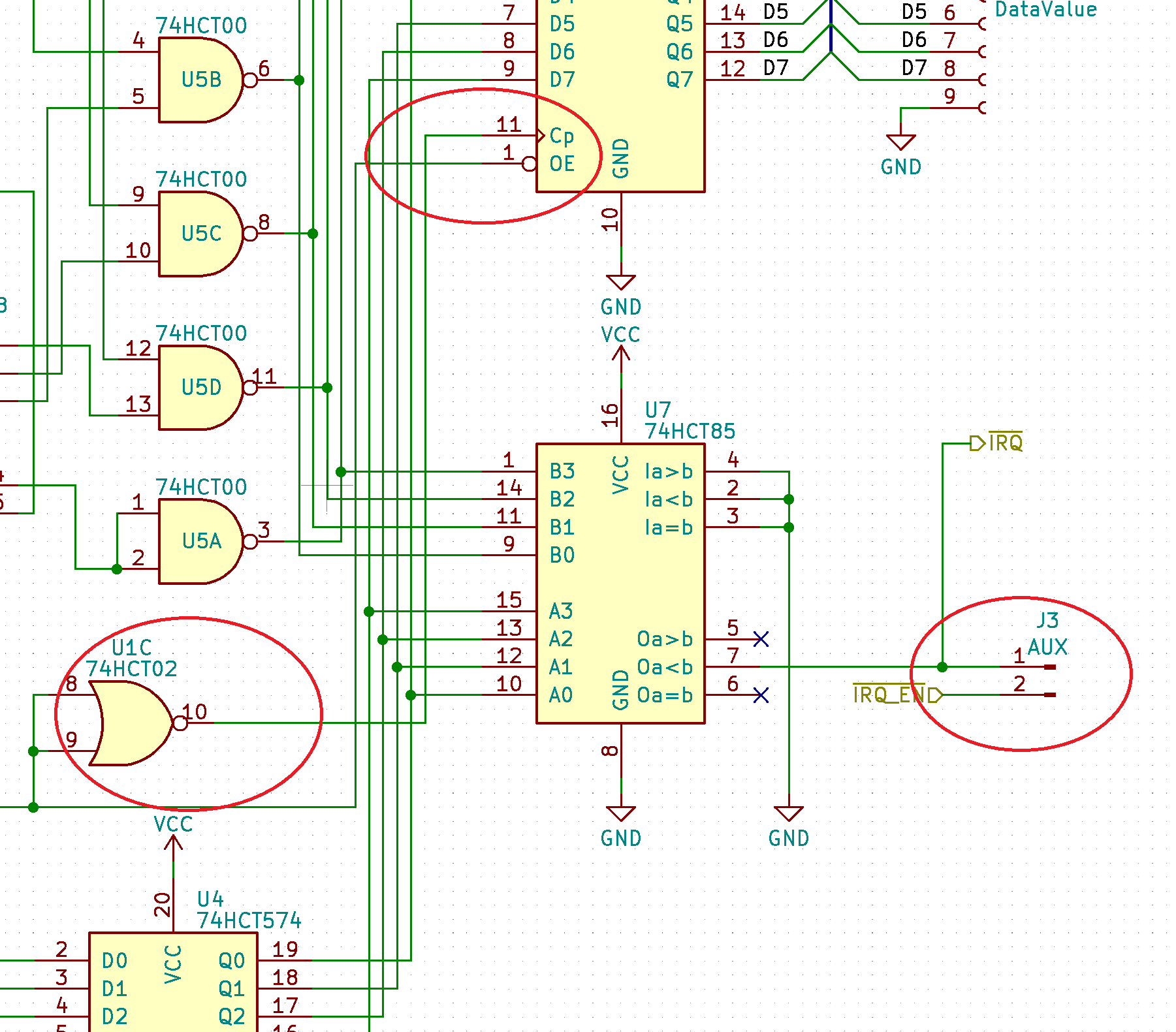
The output (the IRQ signal) is active high and the processor expects an active low signal, so here we got to insert the extra unused NOR-gate to invert it.
The clock pulse was connected to an inverted read signal which means that it will not clock in an released interrupt in the register without reading it again. This was sorted by clocking it with Q, since that is a quarter pulse earlier than the read, it will always have fresh data in the register upon read.
OE was connected to the read signal and since it is an active low input it needed to be inverted. So we reused the NOR-gate used for the previously used clock pulse.
We also found that the NAND gates collecting the irq-levels (U5) was out of order so the interrupts came in in the wrong order.
![]()
-
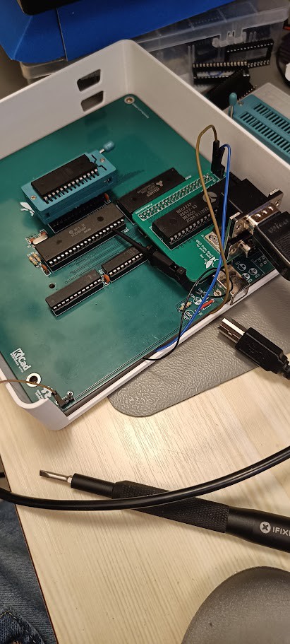
One of the prototypes for stage 2 is tested!
11/08/2024 at 21:45 • 0 commentsMe and my son has tested the prototype for the joystick port controller. I had ordered prototype boards to be able to test the functionality of the joystick controller and the IRQ handler before ordering the stage 2 board.
![]()
We found that I had mixed up the 2 ChipSelect inputs so it was active the entire time, killing the bord. And when I fixed that (by inverting the signal from the logic GAL) we found that 2 of the input pins on joystick A was swapped. I have now updated the schematics for coming stages and will update the uploaded files later this weekend.
Next up will be the interrupt handler!
![]()
-
So I did a thing...
11/03/2024 at 08:41 • 0 commentsSo i decided to make a simple case to protect the board, it is not in any way done or perfect, but it is sufficient for prototyping.