 Eric Lind
Disclaimer:
When I started this journey down the 6809 path I had never heard of the TRS-80 or any of its siblings, I'm European and very much loyal to Commodore, with both C64 and C128 on the desk. In later days I started tinkering with Z-80 and ended up getting 2 Speccys (Sinclair ZX Spectrum). So Z80 and MOS6502/8502 are the only processors I really worked with in the 8-bit universe.
Goal (or what do I want):
So what do I want the final product be? Well as long as me and my son keeps getting better and better ideas it will evolve slightly over time, but in general it will be:
- a micro computer system based on a 6809/6309 microprocessor
- a serial controller with a regular RS232 port and a USB port (This will be the terminal port for debugging and updating etc.)
- a 6522 VIA based dual joystick port (for all your gaming needs)
- 8kB EEPROM for BIOS, drivers and monitor code (size might change if needed later)
- 512kB static RAM with option for 512kB more on board (the system itself supports up to 4MB of RAM)
- fully programmable address and control logic (3 GAL chips)
- a PS/2 keyboard and mouse interface
- interrupt controller for 15 unique and prioritized interrupts (it is also possible to set a mask to hide interrupts)
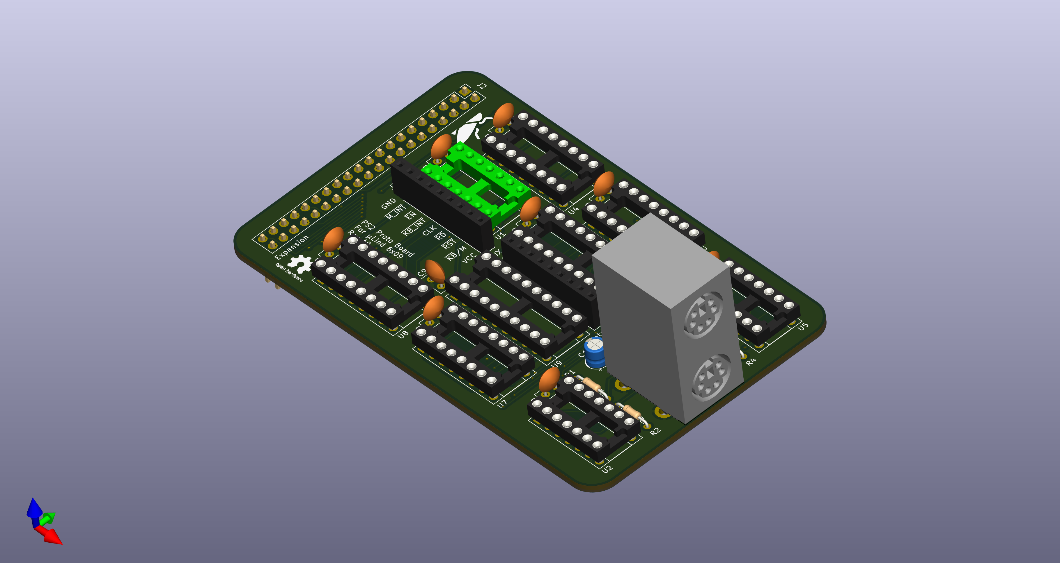
- an addon port for a audio card (I have already designed a SID 6581/8580/Arm2Sid based board and started on a OPL3 based board)
- an addon port for a video card (I have a VDC 8563/8568 based one with 2kB character ROM and a working on a V9958 based one)
- an expansion port with full access to entire address space and all control signals (to be able to implement some smart DMA stuff later on)
- and a CompactFlash card interface for the "unlimited" storage we all dream of.
For the expansion port I have already started to design an similar sized expansion unit, with address logic, place for 2 extra 512kB RAM chips and 5 expansion ports. And I have designed a 24 bit parallel I/O module and started on a IEC interface for connecting Commodore drives to the system.
The beginning:
Soon we had so many ideas that a project started to take form, and I started to draw a possible schematic in KiCad. After some simple testing and "proofreading" by my son I felt that we could be able to make a board of this. I even sat some limitations on the board, just to spice it up a bit, but in the end I had to make it in 3 stages to be able to manage the full scope, it was just too much to put on one board in one go for an microcomputer-rookie like me.
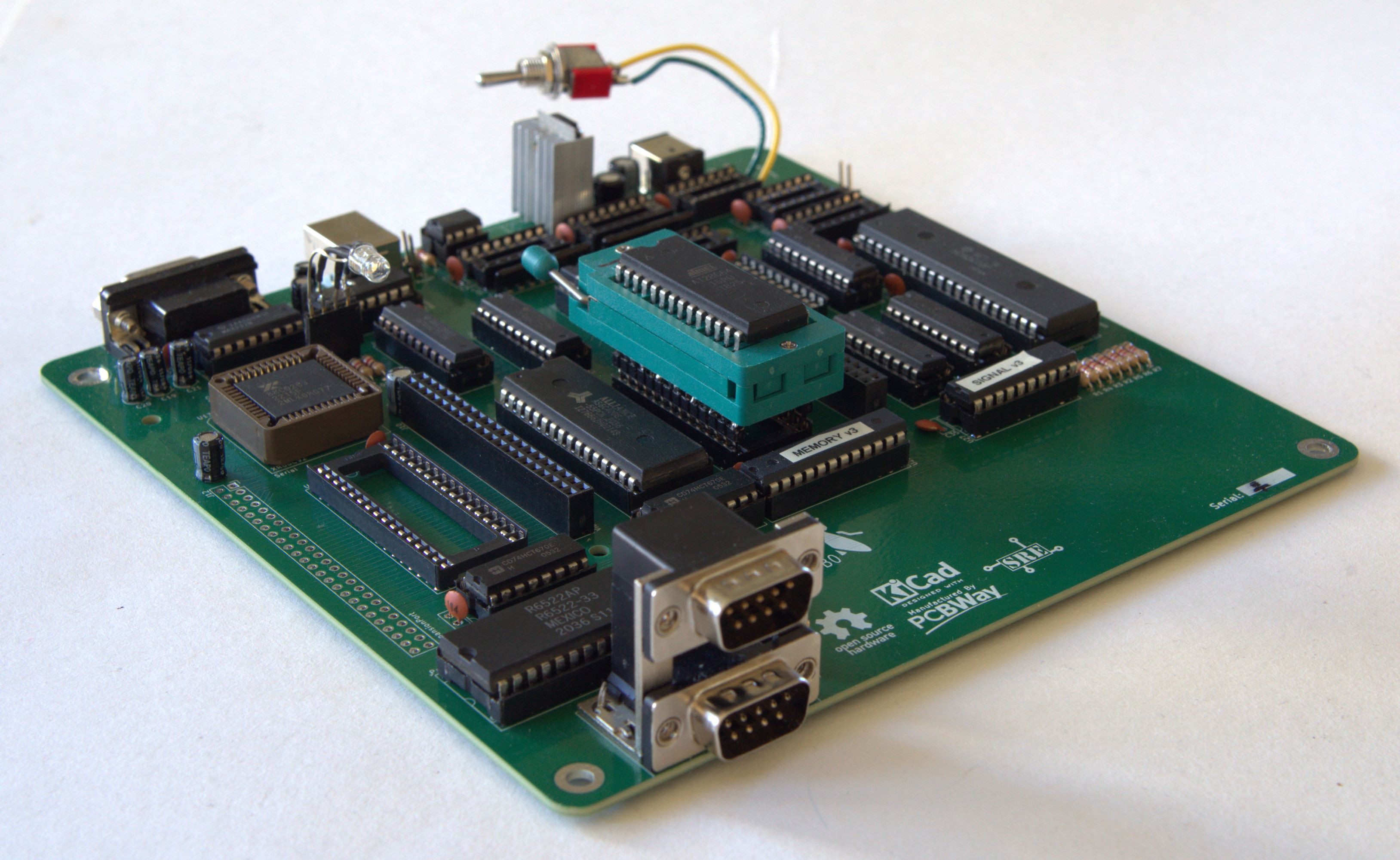
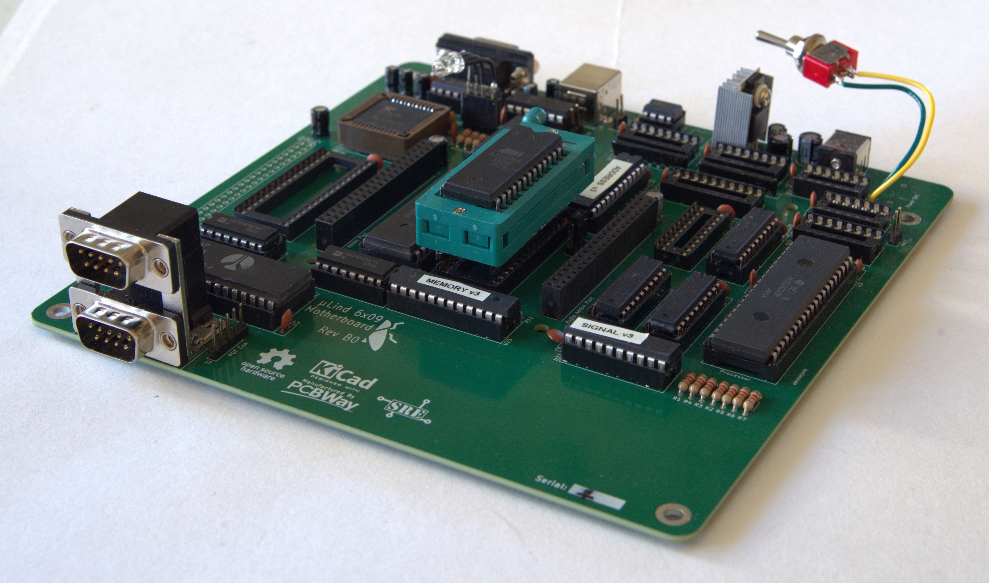
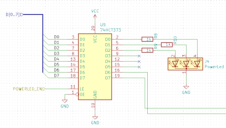
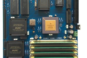
| Stage 1 | CPU, EEPROM for bios and test applications, RAM, address-logic (one GAL16v8), a serial controller and an expansion port. |
| Stage 2 | Stage 1 + Parallel port (6522), complete address logic (2 GAL22v10 and 1 GAL16v8), IRQ handler and addon ports for audio and video cards. |
| Stage 3 | Stage 2 + PS2 interface and CF Card addon port. There was no real estate left on the board for a full size CF socket. |
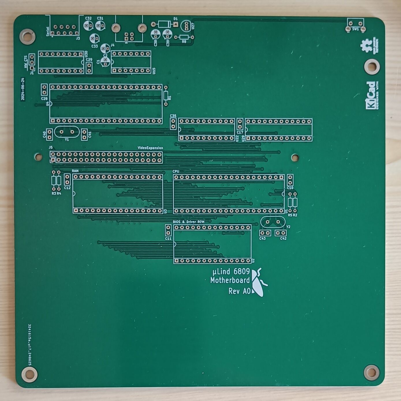
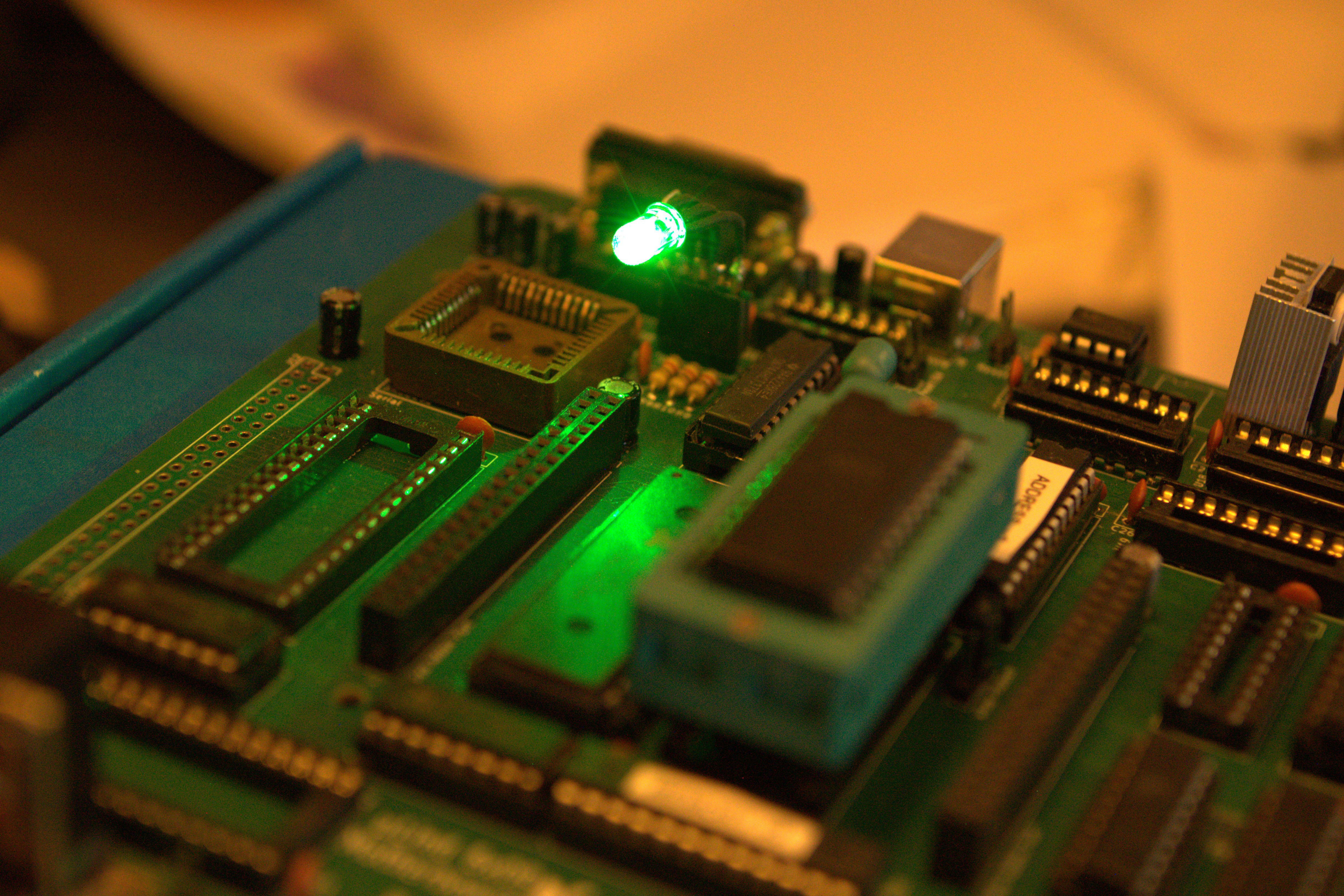
Stage 1 ( status: TESTED):
So stage one was just a basic board with a EEPROM, a RAM, a GAL (for control signals) and a serial chip for communication. This basic board also have a single expansion port to be able to test small (and much cheaper) prototype boards for functions on later stages. This will hopefully let the next stage have lower probability for faults.
After assembly and testing of the stage 1 board, the conclusion is:
- I forgot a pull-up on the DMA/BREQ pin on the CPU.
- The power regulation and reset handling was not very good, has been complete re-drawn in stage 2.
- The serial controller is very slow, is also replaced in stage 2.
- I forgot to pull out the spare pins of the GAL to the expansion header (the prototype boards need to have an ENABLE signal hand soldered to the GAL)
Apart from these points was the first prototype board successful!
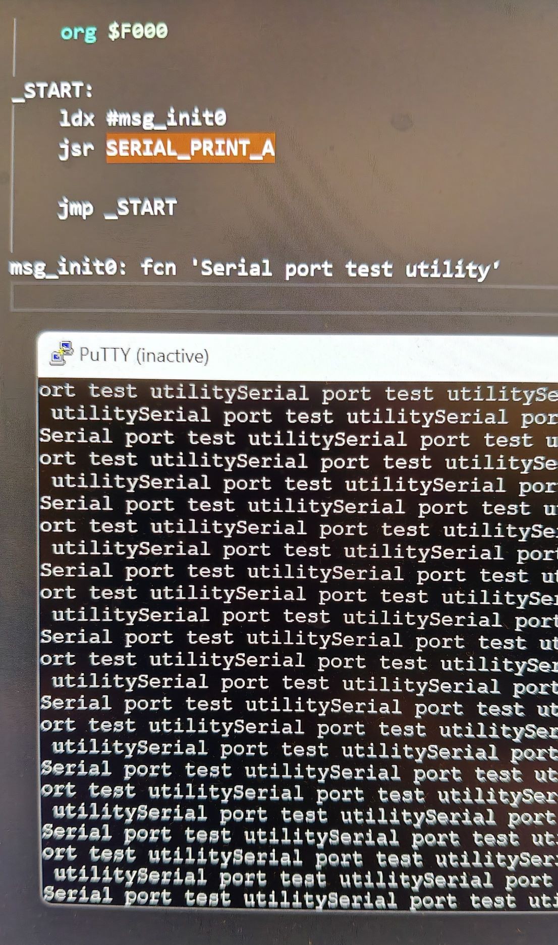
My son managed to write some code that simply echoes a word back when typed in the terminal in just some hours.
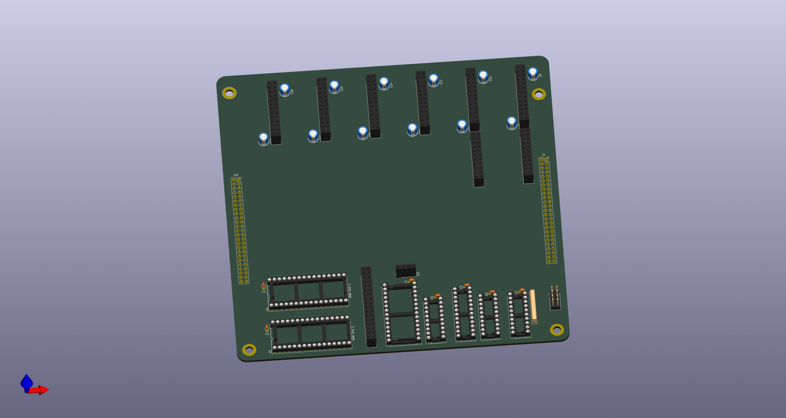
Stage 2 (TESTED and DONE):
The stage 2 is based on stage 1, with some modifications, bug...
Read more »


 Tobias Rathje
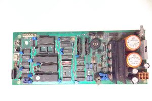
 Ken Yap
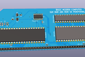
 Gee Bartlett
 Colin Maykish
You might want to consider NitrOS-9 as a multi-tasking OS. It would have to be modified to run on your 6809 board, but it should be doable.