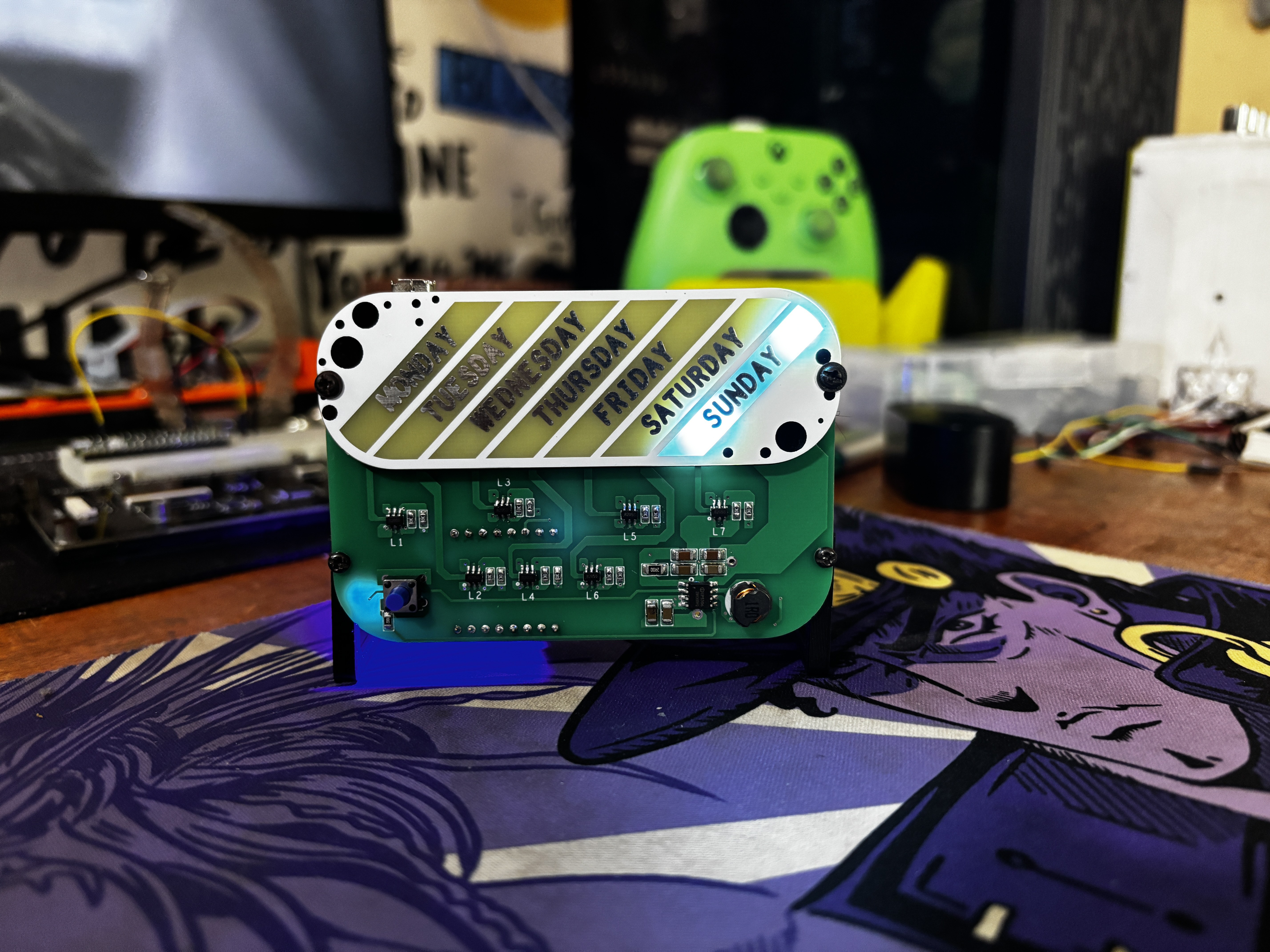
The goal was to design a little desk clock that tells us what day it is.
Here, we're using a completely customized LED driver board, each with three LEDs connected in parallel and driven by a Mosfet IC, which is controlled by the DFRobot's Mini Beetle ESP32-C3. To represent seven days, we used a total of seven LED setups, each having three LEDs connected in parallel with a mosfet IC arrangement.
We also integrated an onboard power source, a 2200mAh 3.7V lithium-ion battery, which powers this arrangement and can be recharged once discharged.
CAD MODEL
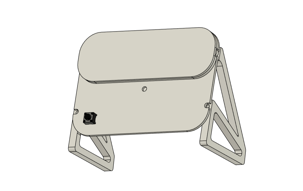
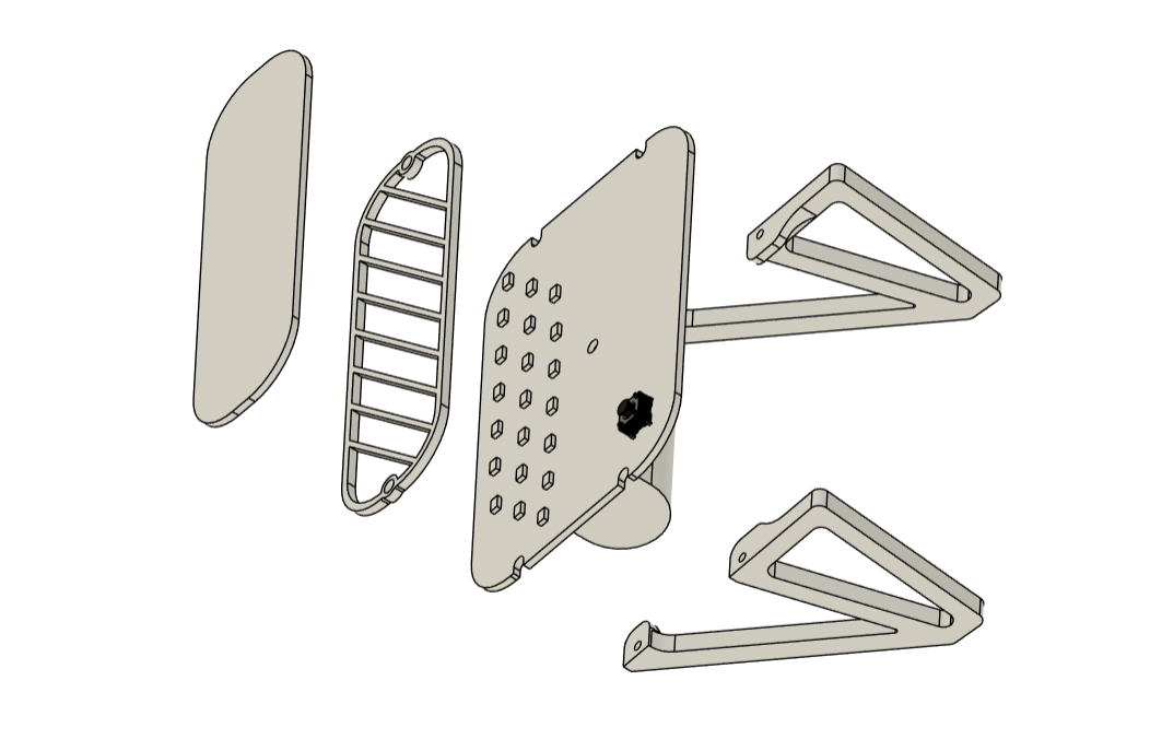
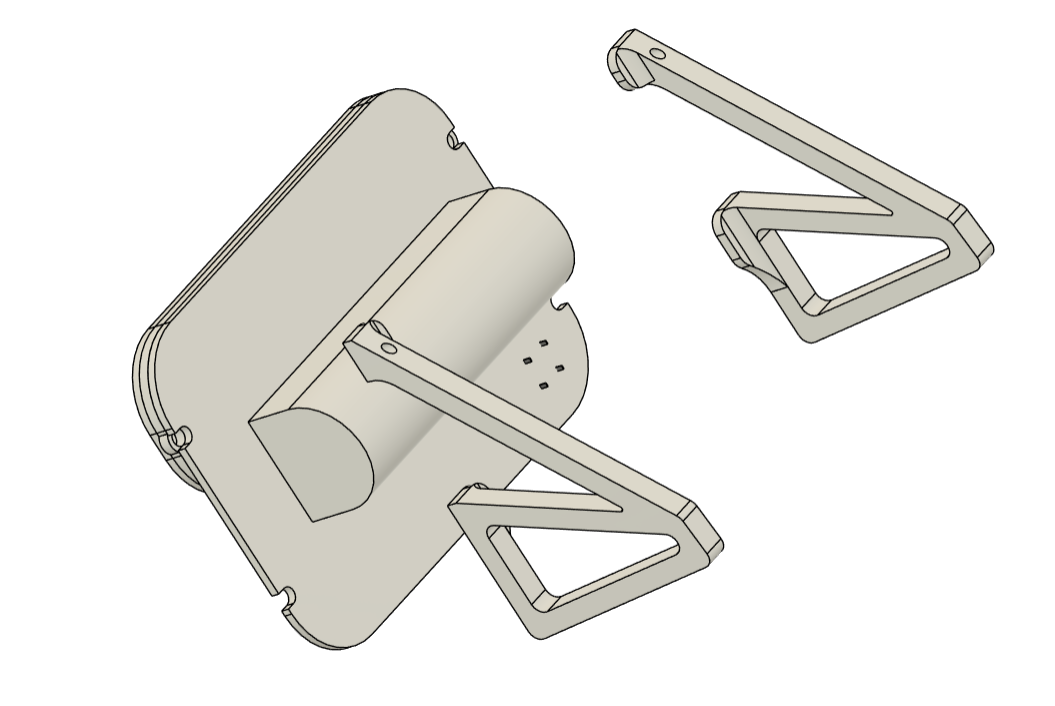
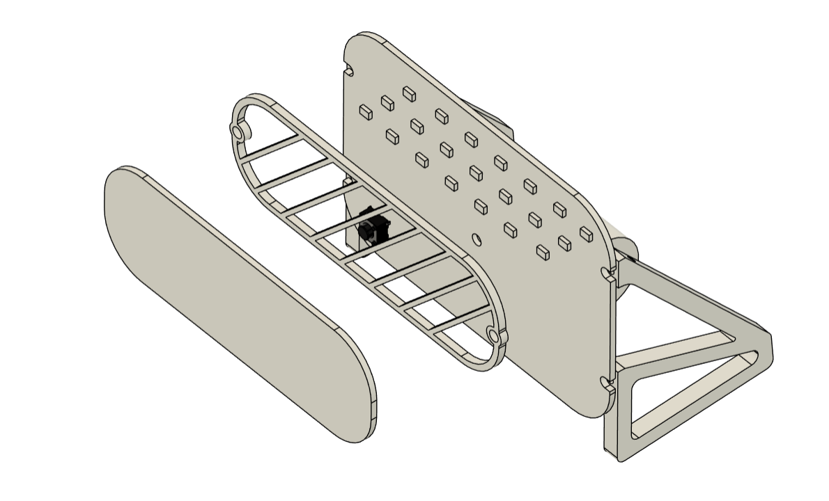
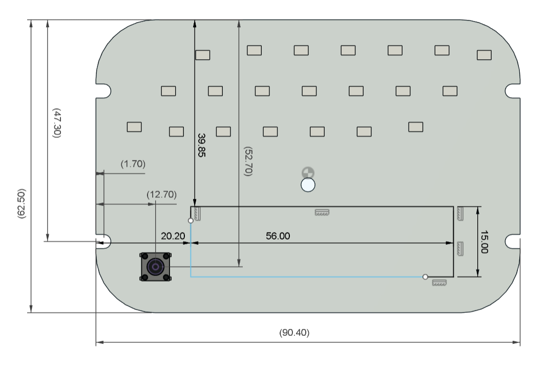
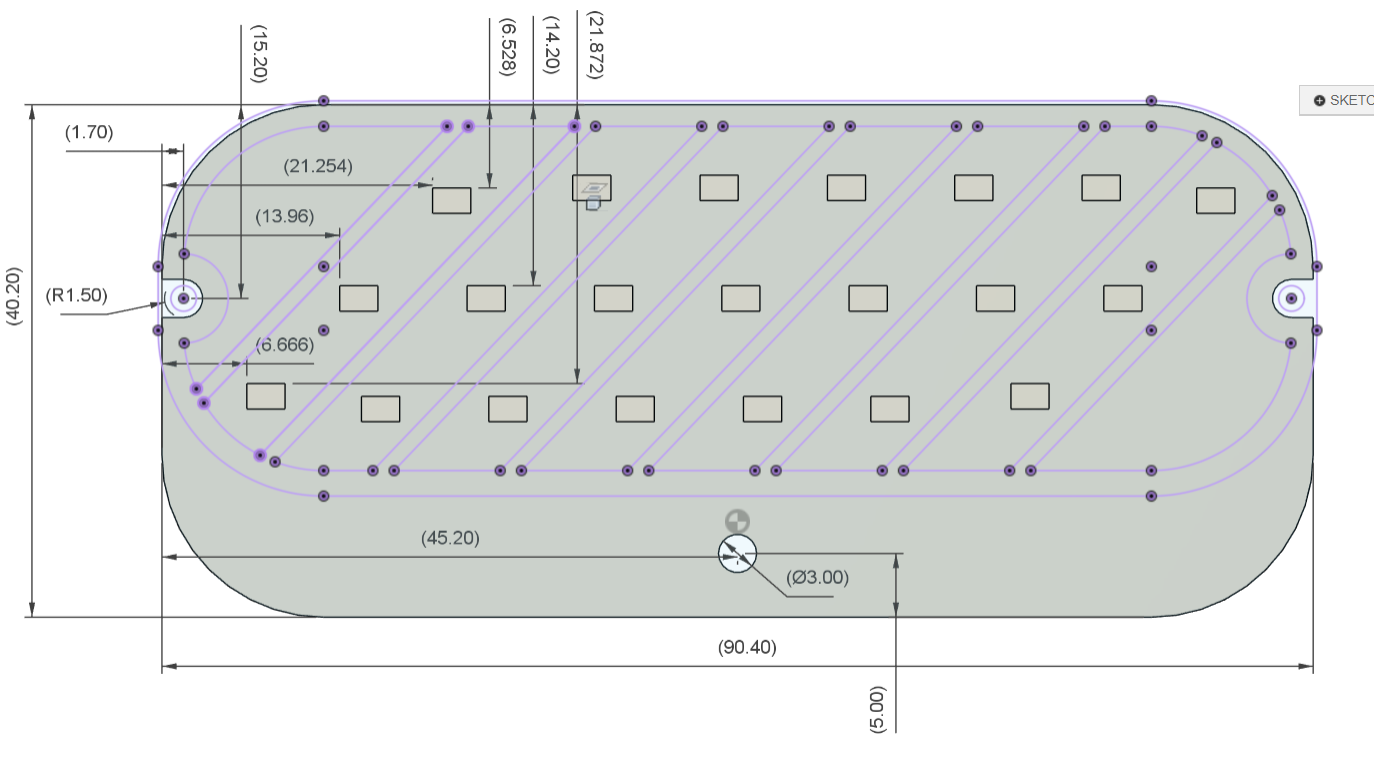
We begin this project by creating a Cad design that consists of a PCB with all SMD LEDs on the top side arranged in a sequence of seven. We place them slightly inclined to achieve the angled effect we want.
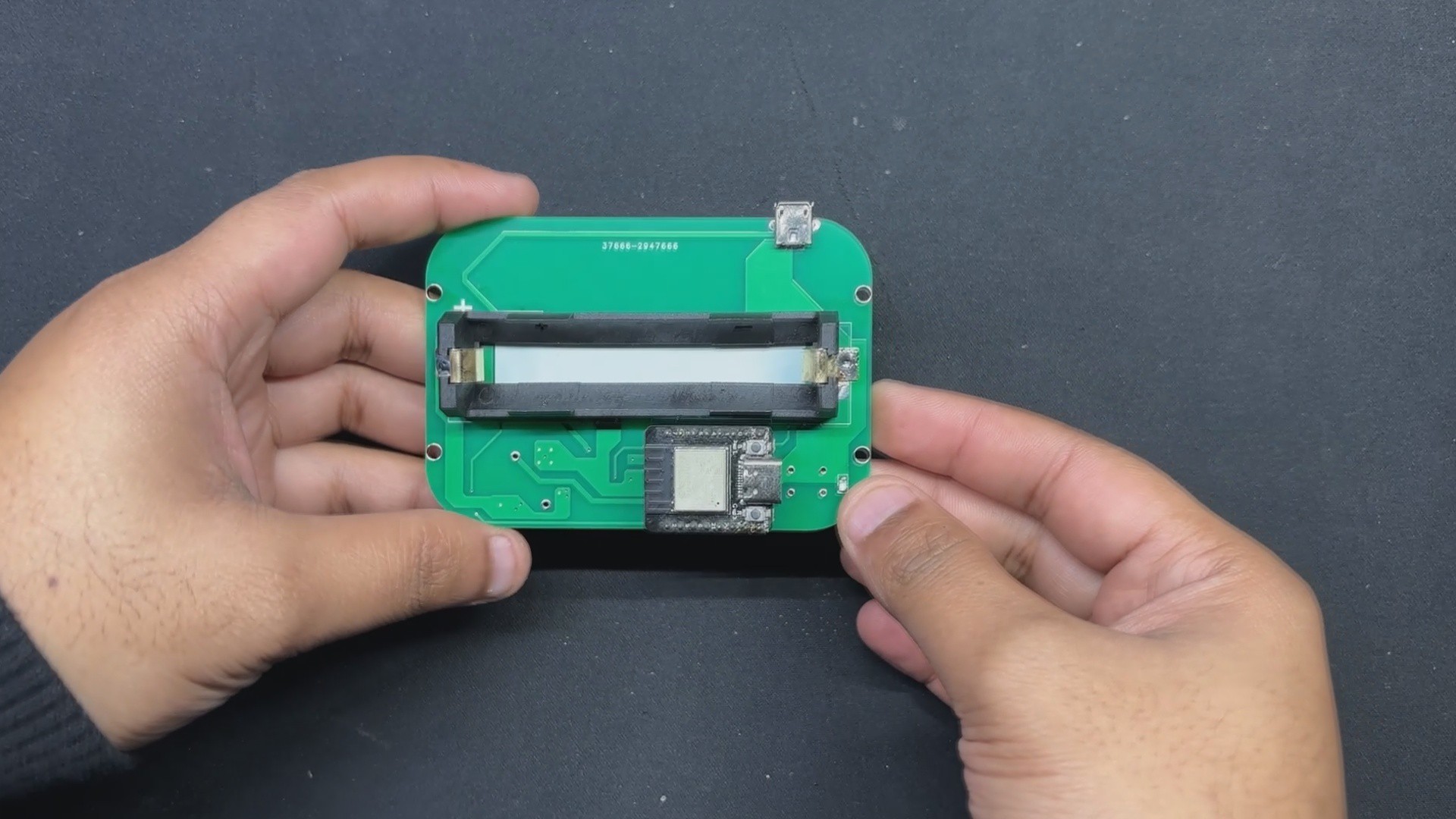
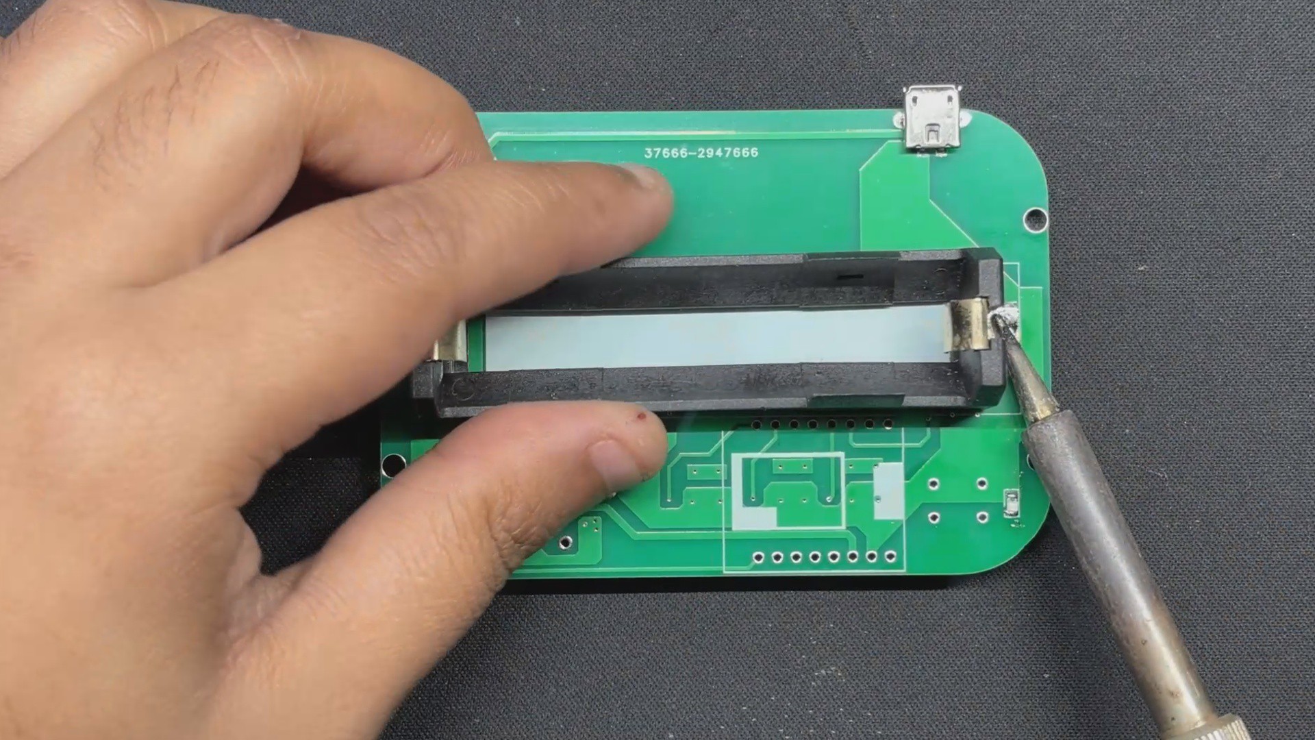
The lithium cell as well as the microcontroller and main throughhole components are all modeled on the bottom side.
We also created two stand-like components to help the clock stand in its proper orientation.
LEDs are mounted on the base or driver board, but their glow is seen on another board that is positioned above the LEDs. This is achieved by utilizing a separator part that creates space between the LEDs and both PCBs.
This design requires three 3D-printed pats, all of which were created using black PLA and a 0.6mm nozzle.
PCB Design
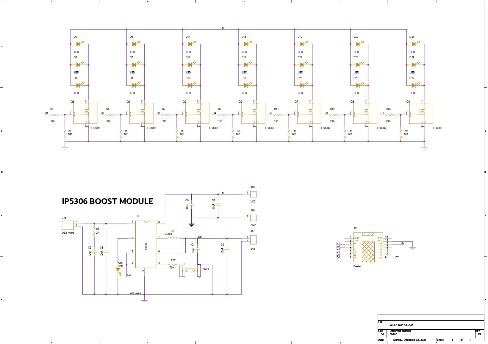
We begin the PCB construction process by creating schematics for the project.
The schematic is divided into three primary parts. The first is the Power Section, which includes an IP5306 Power Management IC configured according to the example layout provided in the datasheet. This power management setup gives a consistent 5V output that our microcontroller and Mosfet IC will use to power LEDs.
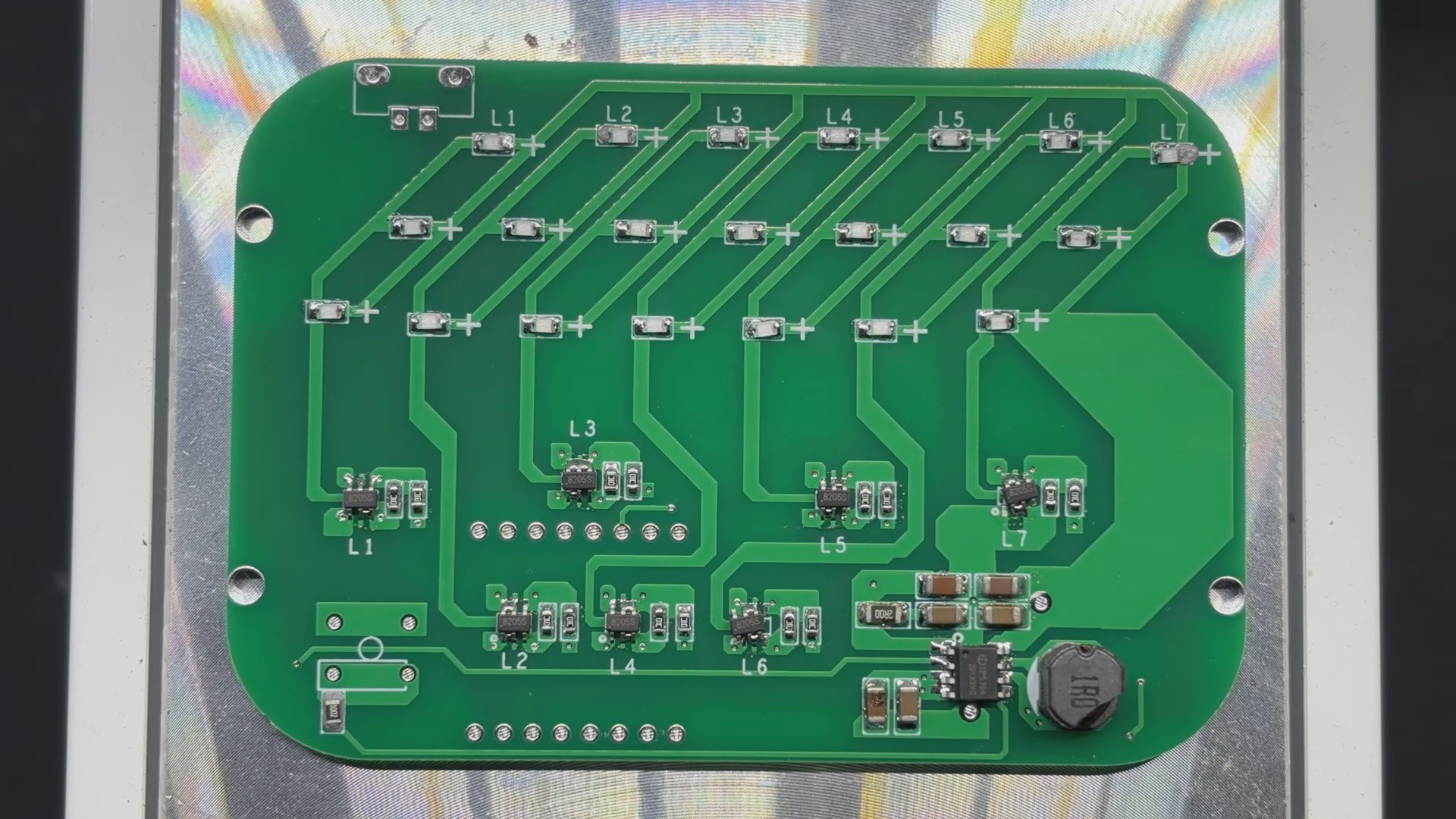
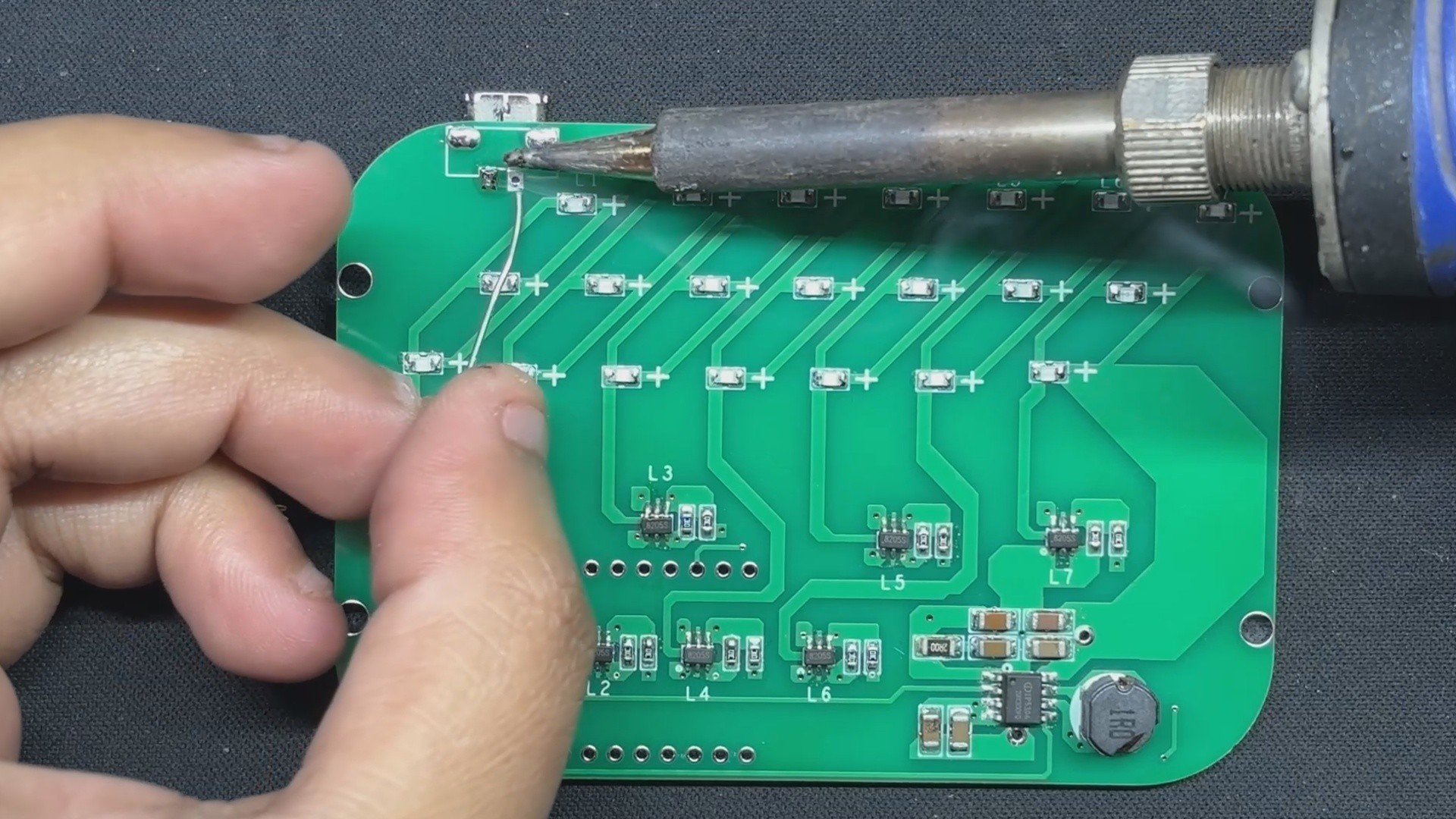
The second section is the LED array. We connected three LEDs in parallel and connected them to an 8205S Mosfet IC whose gate is connected to the microcontroller's I/O port via a 10K resistor. An additional 10K resistor is put between the MOSFET gate and source. This design contains seven LED mosfets, each of which is coupled to a microcontroller I/O pin.
The last section is the DFRobot's Mini Beetle ESP32-C3 Microcontroller board, which is connected to the IP5306's 5V and GND outputs, as well as the gates of each mosfet.
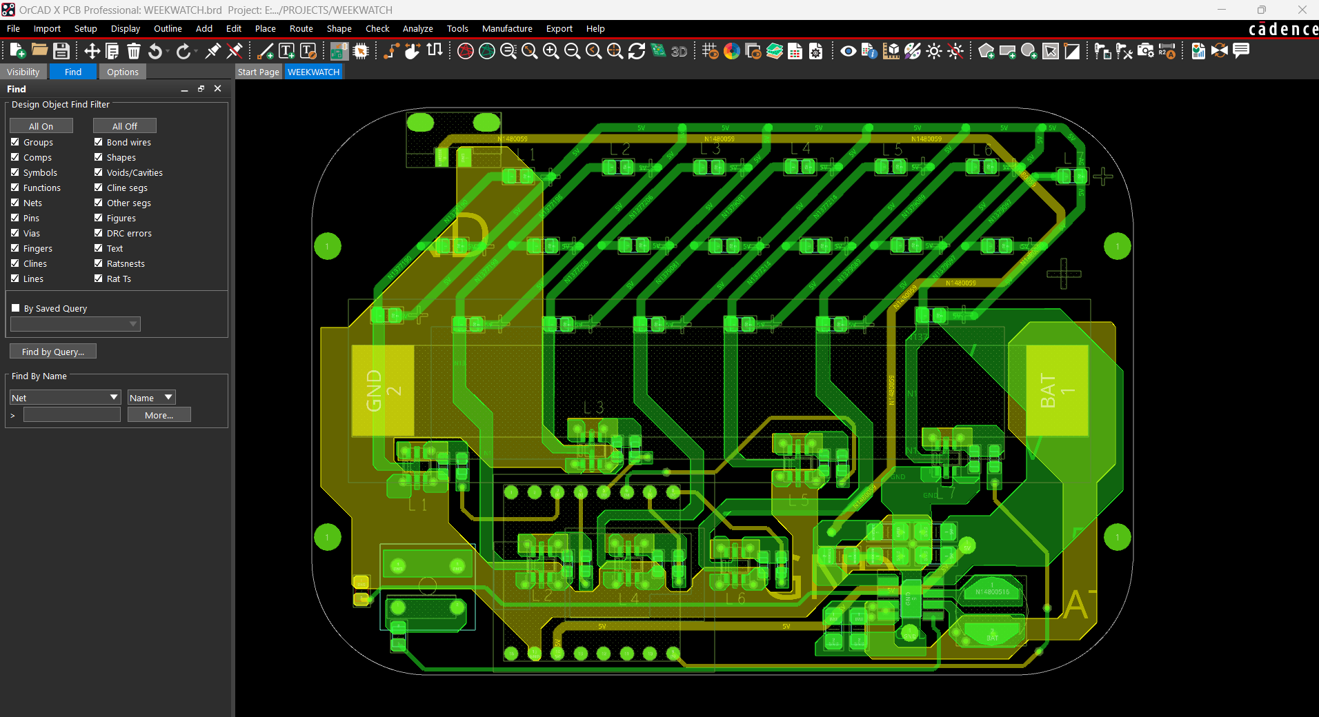
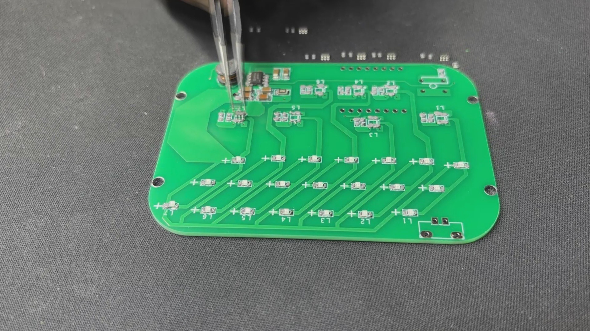
Using the cad layout for the PCB, we then prepare the PCB design for this project, which includes the actual placement of the LEDs. Because we will be putting an additional board over the driver board, LED placement is critical, so we use dimensions from the cad file to prepare the PCB and place components correctly.
We also prepare the Art PCB, which is a half-board with no components and only two mounting holes. We also use the cad file measurements to open the soldermask top and bottom on this art PCB, and we place the names of the days on the TOP layer.
After finalizing both PCBs, we exported the gerber data, which will be sent to a PCB manufacturer for samples.
NextPCB PCB Service
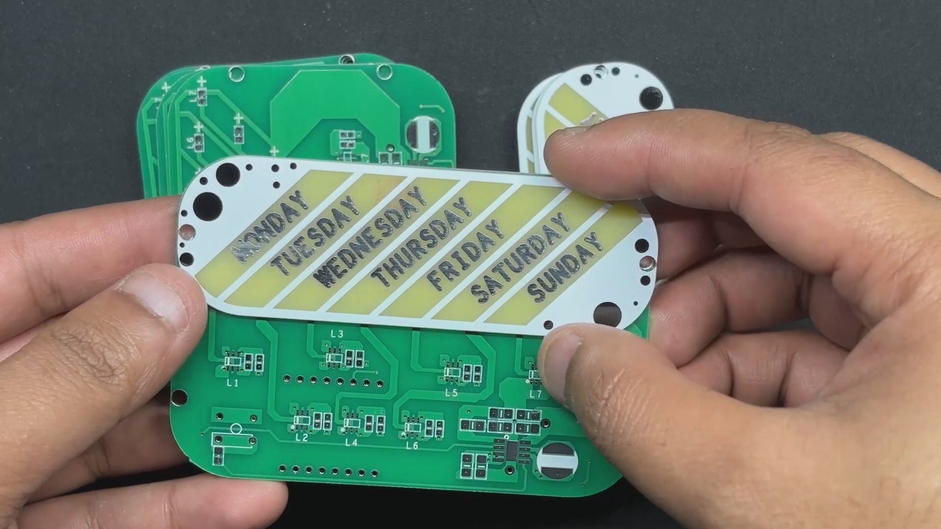
After completing the PCB design, we send both Gerber data to HQ NextPCB for samples.
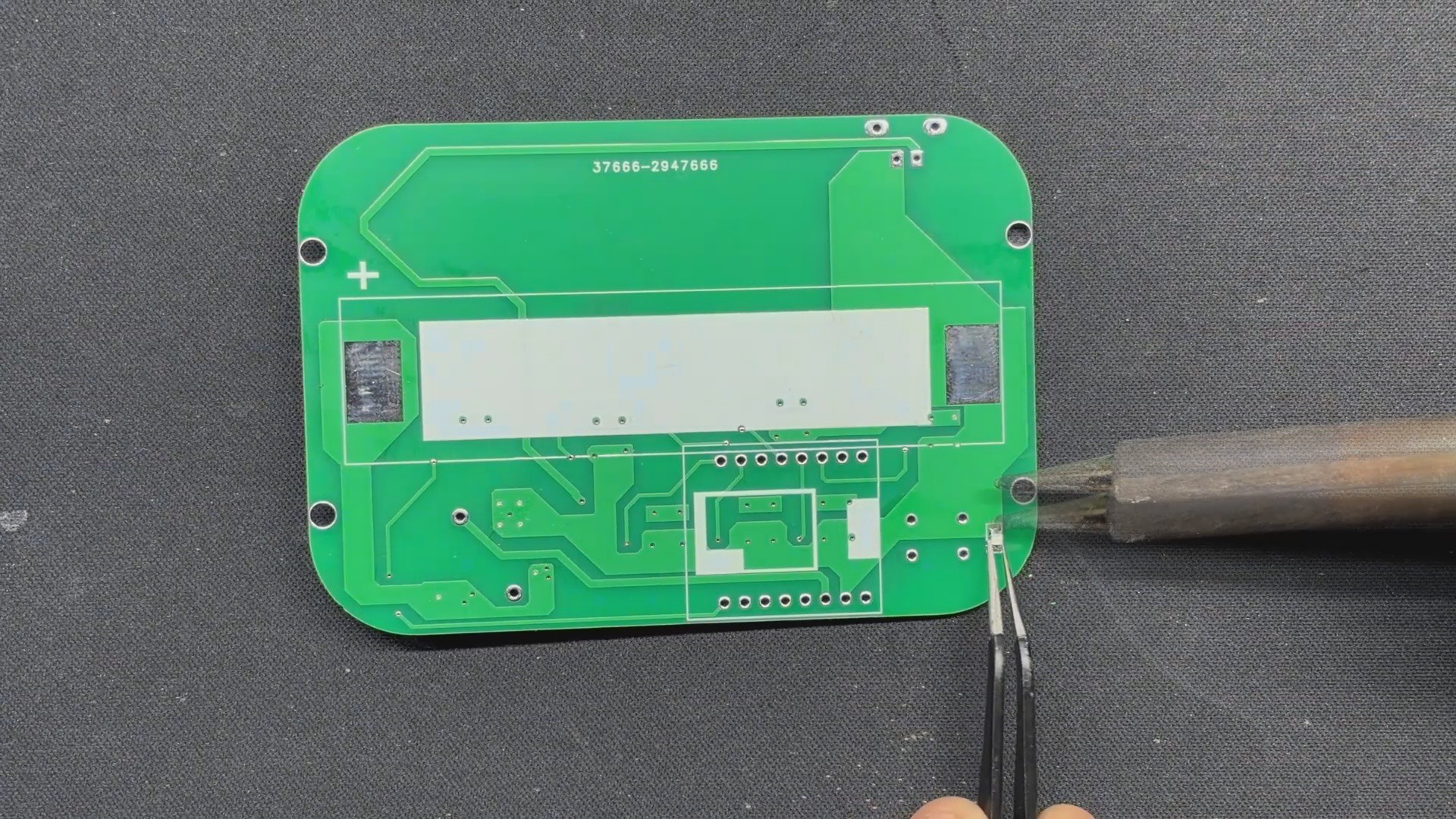
Gerber Data was sent to HQ NextPCB, and two orders were placed: one for the green solder mask with white silkscreen and another for the white solder mask with black silkscreen.
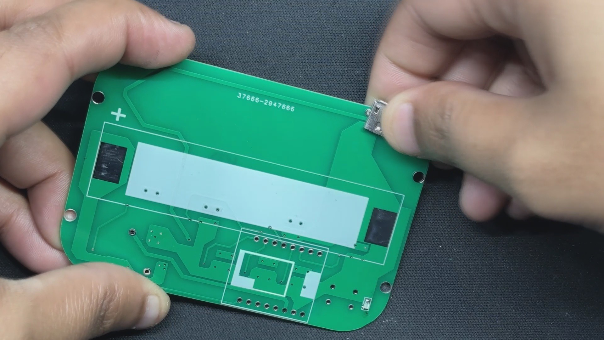
After placing the order, the PCBs were received within a week, and the PCB quality was pretty great.
In addition, I have to bring in HQDFM to you, which helped me a lot through many projects. Huaqiu’s in-house engineers developed the free Design for Manufacturing software, HQDFM, revolutionizing how PCB designers visualize and verify their designs.
Take advantage of NextPCB's Accelerator campaign and get 2 free assembled RP2040-based PCBs for your innovative projects.
https://www.nextpcb.com/blog/rp2040-free-pcba-prototypes-nextpcb-accelerator
This offer covers all costs, including logistics, making it easier and more affordable to bring your ideas to life. SMT services can be expensive, but NextPCB is here to help you overcome that hurdle. Simply share your relevant...
Read more » Arnov Sharma


So True!