Anders Helgesson
-
Where is the logic?
09/26/2025 at 19:47 • 0 commentsI tried dumping the PowerPak after I used it, but it didn't work so I checked the dumps in wireshark, and the mcp2221A GPIO is set to a different state after it's been used.
So I altered my program to set the sram to the same settings as before it's being used. That worked and I could dump the chip.
Doing a diff and analyzing what is different is the fastest way.
8c8
< :10007000000F939010FF7F000000000000000000C0
---
> :10007000010F939010FF7F000000000000000000BF
13c13
< :1000C000F80F01010F0860A800A800177715770442
---
> :1000C000F80F01010F08A0C000A8001777157704EA
16c16
< :1000F0004028100101010BC8A191A35A000008A5D6
---
> :1000F00040A8110101010BC8A191A35A000008A555
This is intel hex data so I'll remove the header and checksum footer. It leaves me with the binary data. There is 16 pages each have 16 bytes of memory, diffs are in pages 7, 12, and 15. Pages are numbered from 0 to 15.
000F939010FF7F000000000000000000 ->
010F939010FF7F000000000000000000
There is a diff in the first byte in page 7(0x70), byte 0x70.Byte 0x70 (registers 903:896):
0b00000000 (0x00) -> 0b00000001 (0x01)
This byte is "CNT2 Counted Value for I2C read" so this have nothing to do with the design of the PowerPAK.
Its just a counter value.F80F01010F0860A800A8001777157704 ->
F80F01010F08A0C000A8001777157704
There is diffs on page 12(0xC0), bytes 0xC6 and 0xC7.Byte 0xC6 (registers 1591:1584):
0b01100000 (0x60) -> 0b10100000 (0xA0)
This byte contains registers for the minimum power selection and UVLO settings for LDO0 and LDO1.Byte 0xC7 (registers 1599:1592):
0b10101000 (0xA8) -> 0b11000000 (0xC0)
This byte contains LDO0 settings, start-up ramping slope selection, and the output voltage.4028100101010BC8A191A35A000008A5 ->
40A8110101010BC8A191A35A000008A5
On page 15(0xF0) there are 2 bytes that diff, byte 0xF1 and 0xF2.Byte 0xF1 (registers 1935:1928):
0b00101000 (0x28) -> 0b10101000 (0xA8)
This byte contains the output values of LUTs or counters.Byte 0xF2 (registers 1943:1936):
0b00010000 (0x10) -> 0b00010001 (0x11)
This byte also contains output values of LUTs or counters.Looking at this the internal design have not changed from the one in the OTP memory.
I suspect they don't change the design in the PowerPAK. They just use the old design, and fix it in software. It would then be a disconnect between hardware, firmware and software. It's like a hardware engineer made a revision of the hardware and a software engineer did the software: They forgot or just left the firmware as is. It's a bit weird.
If this is the case, how do they tell the difference between GSD rev 1.0 and GSD rev 2.0 in software?
I checked dmesg when the GSD rev 2.0 was plugged in.
[748715.863239] usb 5-1: New USB device found, idVendor=2dcf, idProduct=d006, bcdDevice= 1.00
[748715.863253] usb 5-1: New USB device strings: Mfr=1, Product=2, SerialNumber=0
[748715.863257] usb 5-1: Product: GreenPAK Serial Debugger
[748715.863261] usb 5-1: Manufacturer: Dialog Semiconductor
Does this mean the MCP2221A is also didn't have it's firmware updated?bcdDevice= 1.00 <- This should have been bumped to 2.0 for rev 2.0. It would have made it so much easier to tell rev 1.0 and rev 2.0 apart.
The GreenPAK designer software clearly shows it in the information window.
Development Board:
Type: GreenPAK Serial Debugger
Hardware ID: 2.0 <--
Firmware ID: 2.0 <--
I'm pretty sure there is nothing in the MCP2221A so it must be in the SLG46582. But then why not change the internal design to match the hardware rev 2.0?
If they used preprogrammed SLG46582's from GSD rev 1.0, the OTP memory can not changed to add the information. Then it has to be done in software. Let's look at the internal design again for the SLG46582, the I2C level-shifter control.
![]()
Looking at the logic here SEL1 is just not used, it's a left over from the UART design before rev 1.0 probably. Only SEL0 is used to mux between I2C to PowerPAK or Target.
Since SEL0 will not turn the PowerPAK levelshifter on or off, this is perhaps used to know if the GSD is rev 1.0 or rev 2.0. It would be a weird workaround for something that can easily be changed, The flash in the MCP2221A is unlocked, so the bcdDevice value can be changed at any time.
I'm just speculating at this point. I'll have to analyze the USB captures to know for sure.
-
The logic
09/17/2025 at 19:48 • 0 commentsI rearranged the design so it's much more easy to see what is going on inside the SLG46582 PowerPAK.
![]()
Turned the I2C registers into network labels instead to remove a lot of lines, makes it a bit easier to see what is going on. The SEL0 and SEL1 logic was moved into its own area since it's logic is separated from the other logic.
The internal design is nothing like I expected, the NC pin has functionality to it. One of the I2C level shifter control pins are not set up as an NMOS. This can only mean one thing, is this preprogrammed design is an old one? Which is probably the design of GSD Rev 1.0. Quick search online for the user manual for GSD Rev 1.0 and it confirmed that this is probably true. It confirmed the error in the GSD Rev 2.0 manual I found before.
The SEL0, SEL1 and NC Logic
Now before analyzing I have to understand how the logic works inside the GSD PowerPAK. It's hard to reason what happens during analysis otherwise.
Since I want to know what SEL0 and SEL1 does, I'll start looking at the logic that is connected to these pins.
NC, SEL0 and SEL1 is connected to three 3-bit LUTs, 3-L3, 3-L1 and 3-L4.
![]()
NC pin is high when only SEL1 is high.
I2C_ON_PROG is only high when SEL0 is HIGH and SEL1 is LOW.
I2C_ON_LDO is HIGH if both SEL0 and SEL1 are low.
So since no more logic is connected is quite easy to reason about the default implementation we have here.
I2C_ON_PROG pin is set up as a open-drain NMOS. This means that if this pin is HIGH it will sink the VDD/EN of the target PCA9306, turning it off.
I2C_ON_LDO pin is set up as a normal output pin. Now we need to look at the schematics again.
![]()
The LDO level-shifter can not be turned off in this configuration? It shouldn't matter if I2C_ON_LDO is HIGH or LOW? It's powered through VDD anyway.
Looking at the GSD Rev 1.0 level-shifters
![]()
It fits the logic much better. Notice the level-shifter UART pins. NC is UART_ON.
Look at the output here.
![]()
There is a 6 pin header there. But with 2 extra GND. Probably where UTX and URX would have gone if they had added UART.
Here is a board view of the GSD Rev 1.0
![]()
The final design doesn't include the 2 UART level shifters. So the UART lines are probably not routed at all. The schematic is not updated to fit the final design which is weird. I guess the schematics, board design and documentation was managed by different people. It's only way to explain this.
Looking at this it confirms that the OTP memory logic of the SLG46582 on my GSD Rev 2.0 is the GSD Rev 1.0 design. They probably had a lot of preprogrammed chips to use. Now does this mean that the device is reconfigured by software before it's used?
The Error pin
This probably has the most logic connected to it. Let's start from the error pin and go backwards to the source of the logic.
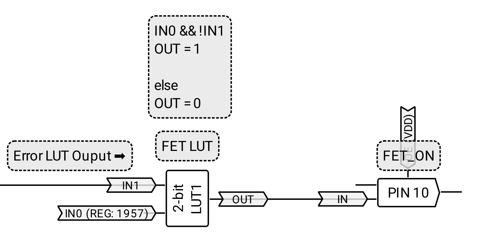
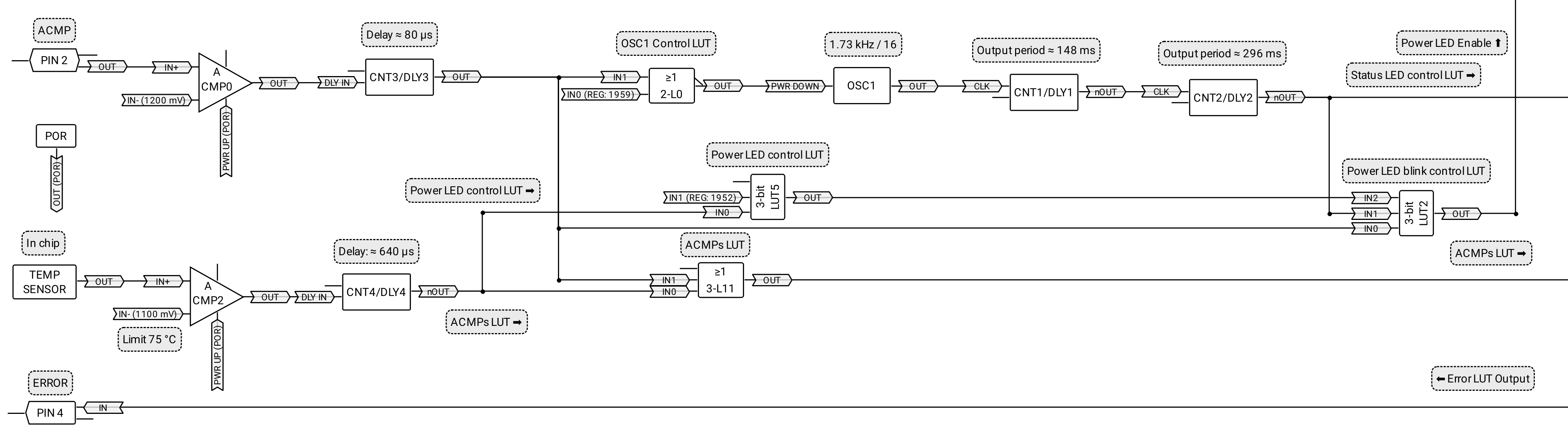
The output of the Error LUT (3-L0) goes to the Error pin (Pin 4), Status LED LUT (2-L2) and the FET LUT (2-L1).
Let's look at the FET LUT (2-L1) First.
![]()
If there is an error, FET LUT output is turned off, FET LUT is controlled directly by the I2C Register 1957.
Next the Status LED.
![]()
Here an error turns off the Status LED.
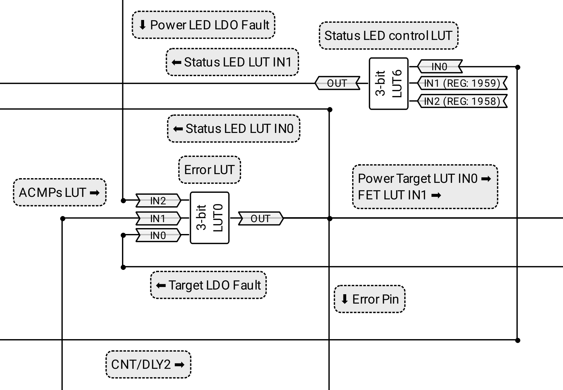
Next is the Error LUT.
![]()
The Error LUT (3-L0). When an error is detected by the logic both the Power target LDO and Target power FET are turned off. The error signals comes from the LDO's themselves (IN0 and IN2) and the ACMPs (IN1). Both overvoltage (ACMP0) and the set temperature limit which is 75 °C (ACMP2).
The status LED control LUT (3-L6). The CNT/DLY2 signal controls the status LED blinking speed. There are two I2C registers connected to it 1958 and 1959.
The I2C register 1958: This controls if the status LED indicator should be on or not.
The I2C register 1959: It controls two things when it's turned on. It releases the powerdown of the OSC1 and enables blinking of the Status LED.
The rest
![]()
ACMP0 is use for overvoltage if overvoltage is detected it will make the power LED blink and activate the ACMPs LUT which signals an error.
ACMP2's output is activated if the temperature sensor in the chip reaches more than 75 °C, it will turn off the Power LED and activate the ACMPs LUT which signals an error.
OSC1 Control LUT turns off the OSC1 if both inputs are 0.
OSC1 has the clock divided down using 2 delays so that you can see the LEDs blink when used.
Here is the complete design in datasheet style with my comments.
![]()
I probably missed something but we should now know how the PowerPAK logic works in the GSD Rev 1.0. Now we have to know how the device is reconfigured for the GSD rev 2.0 hardware. There are two ways this can be done I guess.
- Capture dumps. Analyze them all to try to find when it's reconfigured.
- Use the GSD Rev 2.0 and dump the PowerPAK afterwards.
Since we don't know when it's reconfigured I'll capture the powerpak logic after it's been used. Fastest and easiest route. If they don't reset the PowerPAK between uses the dump should contain the new design.
-
Capturing USB traffic and analyzing it
09/14/2025 at 20:45 • 0 commentsTo know how the GSD really work we need to know all the unknowns of the hardware and capturing the communication between the GSD and the software can provide us with more information.
Instead of using wireshark directly to do the capture I decided to use dumpcap as it is. I wrote a script that is run as root that uses dumpcap on the usb interface the GSD uses, when the capture is over it will move the file over to my user, it renames and adjust the permissions. Then I'll analyze the dumps in wireshark.
Captured two dumps, one when reading a SLG46826V and a full programming cycle for my diavox SLG46826V.
Analyzing gets old pretty fast tabbing between the datasheets and wireshark to see what the bytes and bits does. So I decided to make a wireshark dissector for the MCP2221A.
After researching some more about it, I enlisted chatGPT to do the bulk of the work or so I thought... Cobbling together unfinished lua dissector script with chatGPT for help, got me some more information.
ACMP (mcp2221a GP3) is being used as ADC.
How do you get the ADC data from the MCP2221A?
According to the datasheet it's in the status command reply.Byte 50, 51 = ADC channel 0
Byte 52, 53 = ADC channel 1
Byte 54, 55 = ADC channel 2Pin out description it says ADC1, ADC2 and ADC3 while it also says "3 x (16-bit) little-endian ADC channel values (CH0 LSB, CH0 MSB, CH1 LSB, CH1 MSB, CH2 LSB, CH2 MSB)."
Here is the first status reply I found in one of the dumps.
Status reply
10 00 00 20 78 00 00 00 00 02 00 02 00 02 78 00
10 00 10 28 00 60 01 01 00 00 f1 79 f0 00 00 00
30 00 1b 00 02 27 13 45 03 00 00 26 90 1c 41 36
31 32 00 00 00 00 08 00 01 03 48 02 00 00 00 00
Since bytes 50-55 is the ADC channels we get this.ADC1: 0x0000
ADC2: 0x0000
ADC3: 0x0008
I noticed this that both the Get SRAM reply and Status reply seems to contain the ADC values. Get SRAM command reply have most bytes including the last 32 bytes marked as "Don't care" in the datasheet. Going to have to deal with more don't care and any values later.
Get SRAM reply
61 00 12 04 78 12 88 1c cf 2d 06 d0 80 32 00 00
00 00 00 00 00 00 10 08 00 0a e1 75 f0 00 00 00
30 00 1b 00 02 27 13 27 00 00 00 26 90 1c 41 36
31 32 00 00 00 00 0a 00 00 03 65 02 00 00 00 00
ADC1: 0x0000
ADC2: 0x0000
ADC3: 0x000A
The values are little endian. So the data for ADC3 from status reply above here its has the value 0x0008 which is 8 in decimal. 0x000A is 9 in decimal so the values are close enough. More testing is required. Anyway let's continue.
To calculate the actual voltage we have to know a few things. How many bits the ADC can do, in this case it's 10-bits, the voltage divider k value and the voltage reference.
The maximum value a 10-bit ADC can get is 1023.
The voltage divider has k of 4.666.The formula to get the voltage is
voltage = adc_value / max_adc_value * vref * k
I know from the captured data that the ADC3 is setup with 4.096 V as reference.
First status reply message.
( 8 / 1023) * 4.096 * 4.666 = 0.149 VoltsStatus reply in the middle of the dump
(138 / 1023) * 4.096 * 4.666 = 2.57 VoltsFor the last status replay message in the dump.
(74 / 1023) * 4.096 * 4.666 = 1.38 VoltsNot sure what is going on or if my calculations are correct. I'm sure I set the voltage to 3.3 volts in the greenpak software. Perhaps there is some calibration? I'll figure it out later with some more testing.
The maximum voltage the ADC in this case see handle is
(1023 / 1023) * 4.096 * 4.666 = 19.11 Volts.
Now why is the voltage divider set like this wasting precision?
There is no input protection before the voltage divider, so to protect the inputs of the MCP2221A and PowerPAK from overvoltage the voltage divider is set up like this.The maximum voltage the PTC can handle is 16 volts.
So if you by accident feed 12Volts into the GSD VDD_OUT it will probably not release magic smoke. The zener will sink the current, the PTC trip and the device will most likely it will still work after the PTC cools down.12 Volts on the SDA or SCL pins would release the magic smoke from the level shifter. It's not possible cost wise to protect devices from all the mistakes the users could make.
Let's now look at the first Get SRAM reply using my dissector in wireshark.
GP0 : SEL0
GP0 Settings: 0x10
    ...1 .... = GP0 GPIO Output Logic Value: True
    .... 0... = GP0 GPIO Direction: Output
    .... .000 = GP0 Designation: GPIO operation (GPIO0) (0x0)
This is SEL0 which enabled at the start. It's thus written into the flash of the MCP2221A as a default value. This is most likely the PowerPAK. Have investigate further to know for sure.
GP1 : ERROR
GP1 Settings: 0x08
    ...0 .... = GP1 GPIO Output Logic Value: False
    .... 1... = GP1 GPIO Direction: Input
    .... .000 = GP1 Designation: GPIO operation (GPIO1) (0x0)
This the ERROR pin and it is set up as an input pin so when an error occur in the PowerPAK logic this pin will be high. This would tell the software an error has happened.
GP2 : SEL1
GP2 Settings: 0x00
    ...0 .... = GP2 GPIO Output Logic Value: False
    .... 0... = GP2 GPIO Direction: Output
    .... .000 = GP2 Designation: GPIO operation (GPIO2) (0x0)
This is SEL1 and it is setup as an output which default value is False. Most likely SEL1 is the target greenpak.
GP3 : ACMP
GP3 Settings: 0x0A
    ...0 .... = GP3 GPIO Output Logic Value: False
    .... 1... = GP3 GPIO Direction: Input
    .... .010 = GP3 Designation: Alternate function 0 (ADC3) (0x2)
Here we can see that GP3 is setup as ADC3.
To truly confirm that SEL0 is PowerPAK and SEL1 is the target GreenPAK. I have to check the I2C traffic.
The first I2C write performed does a write to `0xF4` with the data `0b00000001`.
Now the datasheet for the SLG46582 doesn't have the address bytes in it like the SLG46826. First convert the 0xF4 to decimal, then multiply by 8. Which is 244 * 8 = 1952.
In the datasheet for the SLG46582 register 1952 is the least significant bit of the byte containing all the I2C virtual inputs. `0xF4` is the byte that contains all these I2C accessible registers which can be used in the logic inside the PowerPAK.The data written to this address is `0b00000001` and since no mask is set this sets registerbit 1952 to 1 and the rest to 0. This could mean either that only the 1952 registerbit is used or that they are just initialized like this.
In the SLG46826 byte 0xF4 is reserved and not used.
This confirms that SEL0 is the PowerPAK, which means that SEL1 is the target.The last unknown is how the logic is wired inside the PowerPAK. To get this I can just use my generic mcp2221a driver change the PID and VID in it to target the GSD and do the dump command in my CLI software. Don't need add GPIO support in my software even as it starts with SEL0 set true.
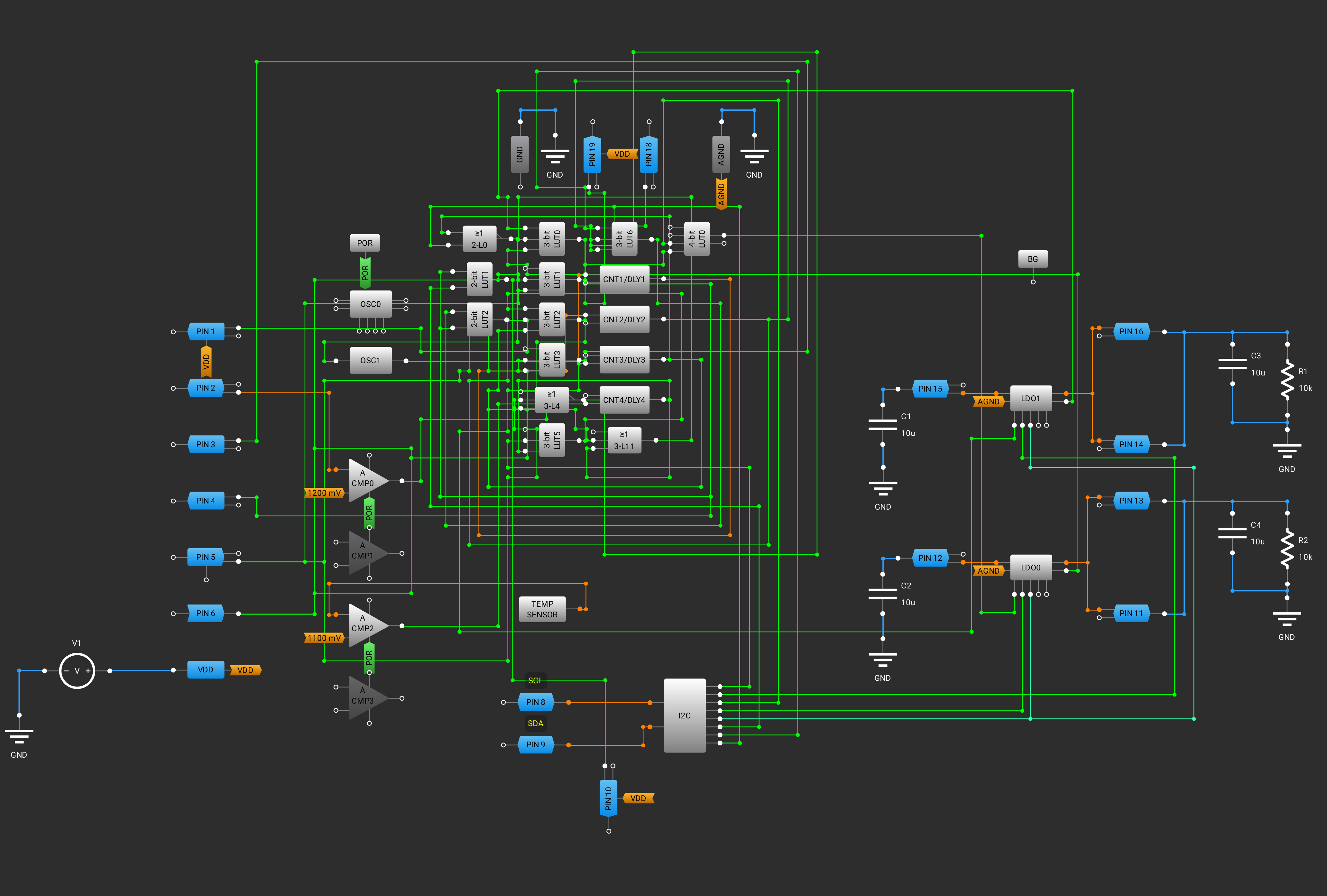
I managed to dump the SLG46582 it was not read locked and feeding it into the greenpak designer software give us this.
![]()
We now have all the data required to exactly know how the GSD works in hardware, but that looks like a mess.
Next time I'll reorder the logic and add labels, so it's easier to see what goes on inside the SLG46582.
-
Starting
09/08/2025 at 20:13 • 0 commentsI do not have to start from zero for this one. The GreenPAK Serial Debugger does also use the MCP2221A USB to I2C bridge. This is the second time and probably last time I will work with the MCP2221A. The reason is simple, lack of documentation of how the I2C engine works.
The MCP2221A datasheet has a lot of "Don't care" "Any value" in it. It turns out that there is a lot of codes not documented for the I2C engine state. If these didn't really matter I wouldn't have a problem with it. But to properly use the I2C engine you need to know them. Instead of being open and sharing how it really works, they keep it like a blackbox for some reason that I'm not going to speculate in.
The offical linux driver even uses undocumented I2C engine state codes. So there is a secret datasheet for the MCP2221A mostly likely where it's all documented.
Long story short, it cost me a lot of time and greif working with the MCP2221A because of it and it's the reason I can not recommed this chip. So I "Don't care" about the cheap price, I will "Any value" something else if I need a USB -> I2C bridge for some other project.
I will call the GreenPAK Serial Debugger GSD from now on.
So how can I make a driver for the GSD?
I have to know how it works. This can be done through reverse engineering.
The GSD is more advanced than my MCP2221A + Level shifter design. The user manual for the GSD contains a schematic it tells you quite a bit how it works.
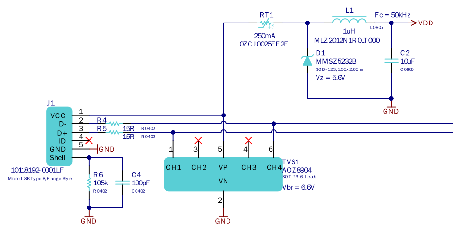
I'll start with the USB side it looks like this.
![]()
The USB connector shield is connected to a 105 kΩ resistor in parallel with a 100 pF capacitor to provide a controlled ground reference, improving EMI suppression and diverting ESD without creating ground loops.
The D− and D+ lines pass through 15 Ω series resistors for impedance matching with the MCP2221A, improving signal integrity and reducing reflections. A TVS diode is used for additional ESD protection. D- and D+ lines are connected to the MCP2221A (not in image).
VCC goes through a PTC to limit the current to 250mA, a zener-diode clamps any overvoltage, and a LC filter is used to reduce noise before going to VDD.
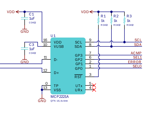
On the MCP2221A side.
![]()
The MCP2221A is setup to be powered by the USB. This uses the internal 3.3 Volt LDO for the USB Transceiver, which is why VUSB is connected to ground through a 1uF capacitor. This means that the I2C and GPIO is working at 5 Volts.
1k Pull up resistors are connected to the SCL, SDA and RST lines.
The 4 GPIO pins used and they are named ACMP, SEL1, ERROR and SEL0.
To know more about what these does I have to look at another part of the schematic.
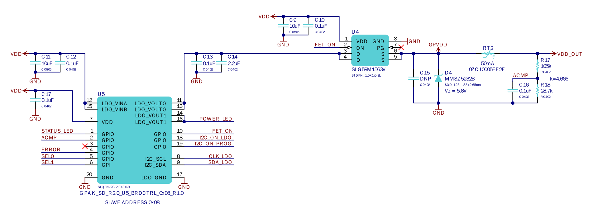
![]()
Looking at this part of the schematic there is a GreenPAK which is a PowerPAK SLG46582, a PMIC with 2 LDO's and configurable logic. The PowerPAK and it's LDO's are powered from the VDD at 5 Volts.
Here I can see that ACMP, ERROR, SEL0 and SEL1 which is connected to the MCP2221A. However the ACMP is also mentioned in the right of this schematic next to the VDD_OUT, does this mean it's connected both to the MCP2221A and PowerPAK?
The user manual also have a pcb layout file but it only shows the top layer with the bottom layer under it, it's not possible to see from this how it's connected.
User manual also says "The connected chip can be powered from the GSD or from an external power. GSD can deliver voltage from 0.9 V to 5.0 V with a maximum output current of up to 50 mA.", "GSD detects the external power and switches off its VDD line (in this case, I2C pull-up resistors will be connected to the external power supply)."
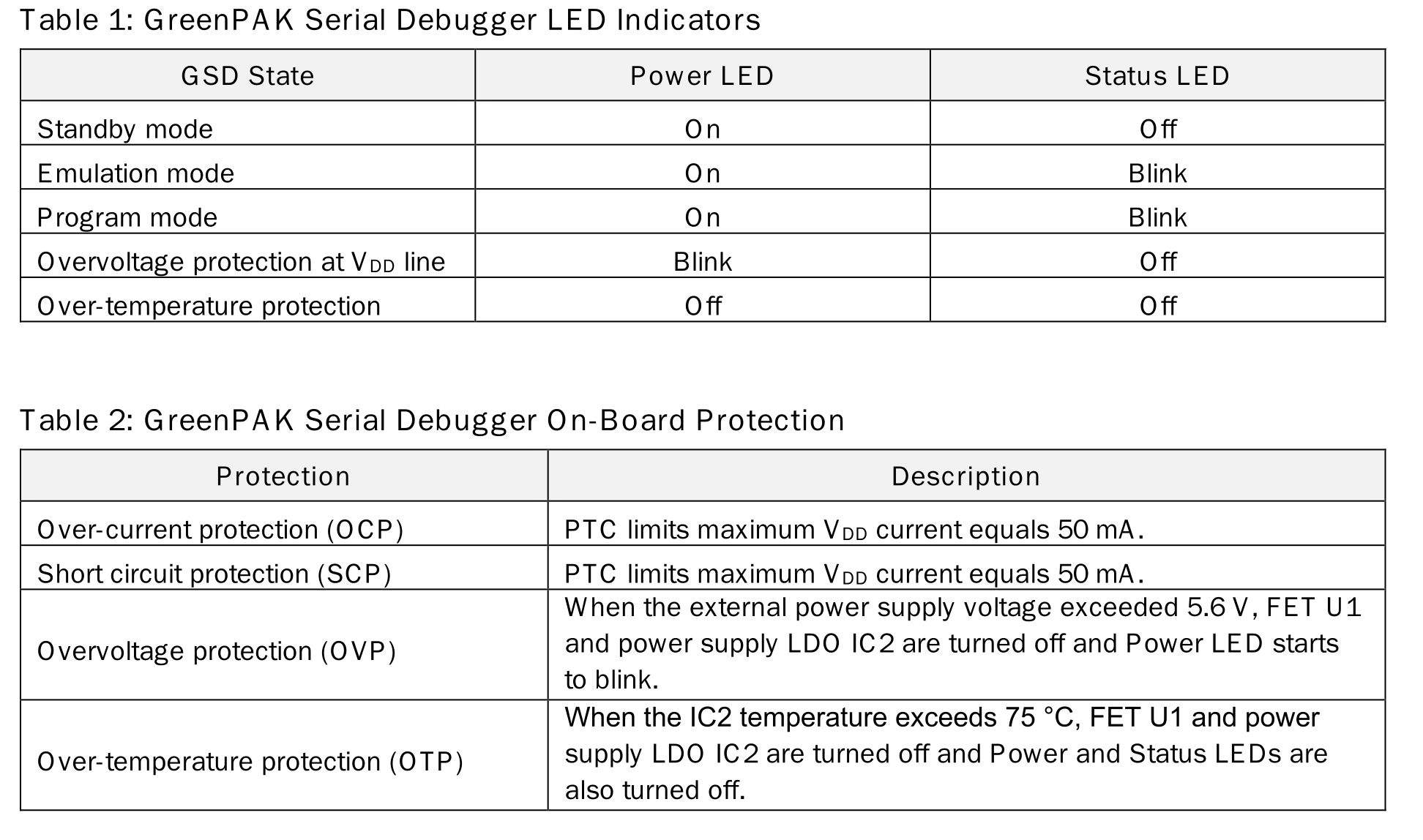
There is also two tables that show how the GSD LED indicators and protection features works.
![]()
OVP and OTP is most likely handled by the PowerPAK with ACMPs and the internal temperature sensor. Some things is a bit confusing here power supply LDO IC2? FET U1? The FET is U4 in the schematic and PowerPak U5, was this a copy paste job from GSD Revision 1.0?
I looked at the board and ACMP is connected from the voltage divider on VDD_OUT to both the PowerPAK and MCP2221A. Since the GSD manual mentions if there is external voltage on the target connector it will turn off the internal power suppy. So the software uses the MCP2221A GP3 pin ADC to read the voltage of the target connector to see if there is external power in the circuit.
If VDD_OUT is powered from the external circuit instead of the internal LDO, it goes through the protection Over-current Protection(OCP), Short circuit SCP and Overvoltage protection (OVP). This fully protects the GSD and there is also an TVS diode on the target connectors. Well thought out design.
Looking at the board I saw that the D- D+ traces are curved not angular and have matched lengths for impedance matching and signal integrity. Nice.
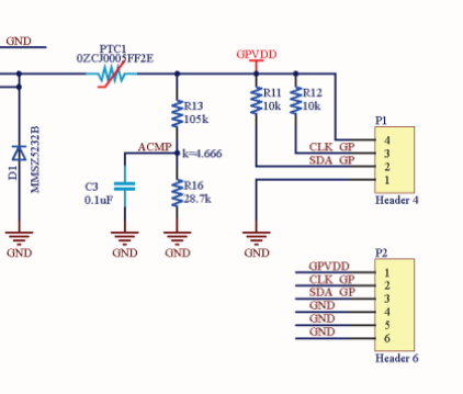
LDO 0 is connected to a load switch which is used to power GPVDD and VDD_OUT from the PowerPAK. The PowerPAK controls the power and status LED's as well.
ERROR pin probably signals the MCP2221A that an error has occured in the PowerPAK logic and that is probably polled by software.
This leaves SEL0, SEL1, I2C_ON_LDO and I2C_ON_PROG.
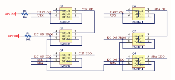
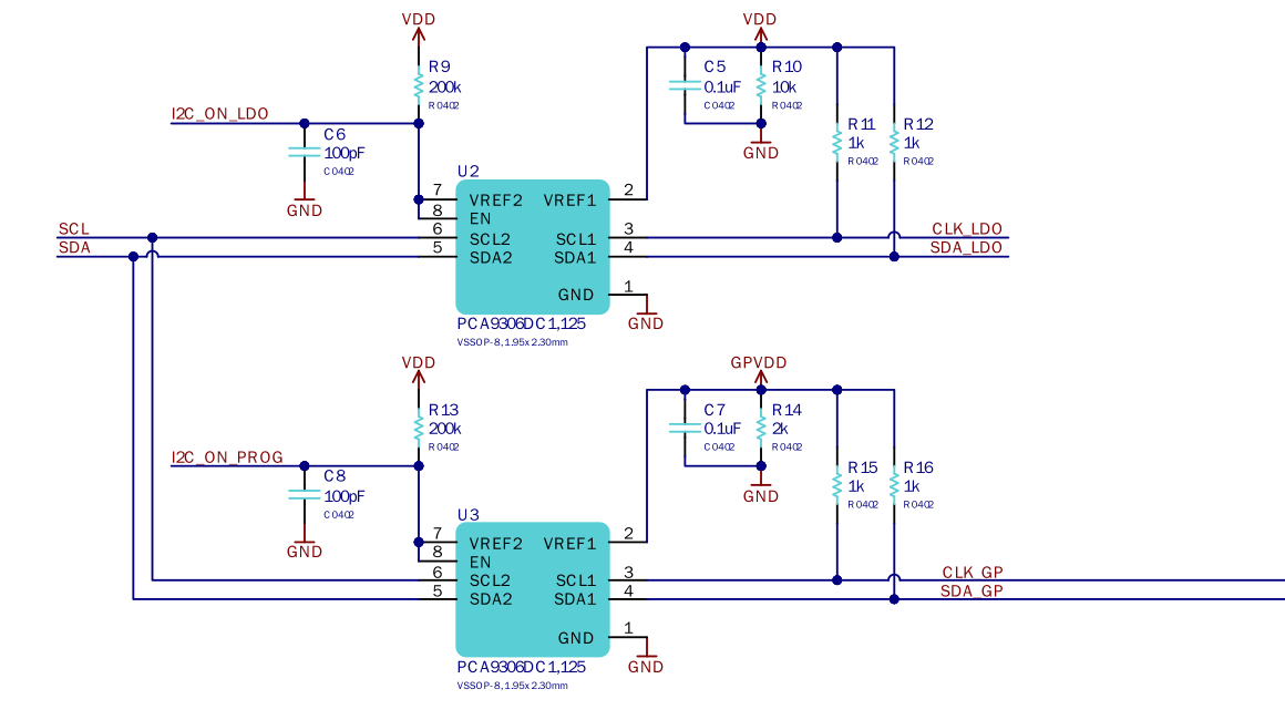
Next is the I2C part of the circuit with two PCA9306 I2C voltage-level translators.
![]()
Here we can see that both level translators are controlled on the high side by the PowerPAK, it has NMOS functionality on it's GPIO pins, so it probably sinks VDD to ground using that.
The PowerPAK controls the muxing between these voltage-level translators using SEL0 and SEL1 pins on the MCP2221A. Which one is which can not be determined by looking at the schematic. How the I2C_ON_LDO and I2C_ON_PROG is connected is set in the configurable logic inside the PowerPAK.
The software can thus communicate with either the PowerPAK or the target at anytime using the MCP2221A GPIO to mux between them.
The 200k resistor and cap is for the PCA9306, looking at the datasheet it says this:
"For the bidirectional clamping configuration (higher voltage to lower voltage or lower voltage to higher voltage), the EN input must be connected to VREF2 and both pins pulled to HIGH side Vpu(D) through a pull-up resistor (typically 200 k ohms). This allows VREF2 to regulate the EN input. A filter capacitor on VREF2 is recommended."
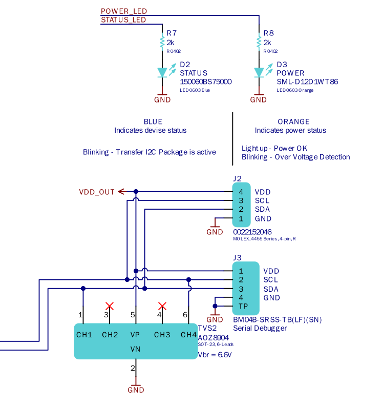
Here is the last part of the schematic.
![]()
The target side has 2 different connectors and a TVS diode for additional protection.
Now I have a pretty good understanding how the GSD hardware works, and the only unknown is the logic inside the PowerPAK.
Next I will capture some GSD USB traffic to analyze and see which voltage-level translator is controlled by SEL0 and SEL1. When that is known I can make the driver communicate with the PowerPAK and try to dump it. If in luck it's not read locked.
Open-source GreenPAK CLI tool + GSD driver
This is a feature creep that wouldn't just go away. This project is a CLI tool for GreenPAKs using the offical GreenPAK Serial Debugger.