 roelof4
Although some of the components used are no longer manufactured there seems to be plenty of 'old new stock' available through the various marketplaces online.
The system design philosophy was to create an eurocard based system with DIN41612 connectors which was very popular in the 1980s in Europe to create systems. Commercial systems at the time where Gespac, PEP Modular Computers, EuroCUBE Celeste and Eltec. The Elektor magazine also published an Eurocard system running FLEX (EC68). There were also many systems developed by hobbyists and I got inspired by the nice UniFLEX system developed by Kees Schoenmakers (https://github.com/kees1948/UniFLEX).
I focused on using only 5V logic but avoided the usual forest of TTL chips and a PAL/GAL solution for the glue logic. Instead I used two 5V CPLD devices which are fast, cheap and can hold a lot of logic allowing one to add some nice features to the system such as fast memory to memory DMA but also esoteric ones like a hardware CRC calculation of OS9 modules. In the File Section I have placed Python code that highlights how to create the CRC calculation in hardware. I used it during testing of the Verilog code. With in-circuit (re)programming system development & testing is quick without having to remove devices from the PCB.
Source code for both UniFLEX and OS9 level II is available, something we could only dream about having in the 1980s since both hardware and software were rather expensive. Full details will be made available through my Codeberg GIT.
The system closely matches the CMS9639 from the 1980s which was similar to the GIMIX III board. Thanks to the SARDIS technology website (https://sardis-technologies.com/oth6809/cms.htm) there is a lot of information on these nice systems.
The addition of a dedicated ethernet interface offers opportunities not available in the 1980s.
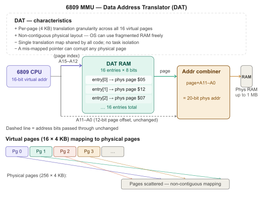
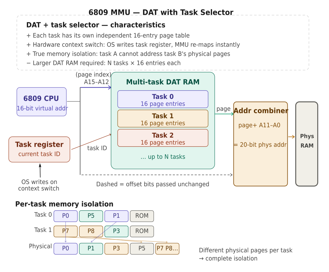
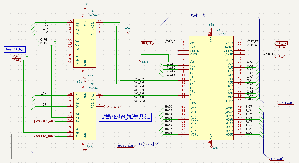
The CPU board is the heart of the system and combines CPU with 1Mbyte memory, (EP)(EE)ROM, console port, ethernet, MMU. Thanks to a EPF10k20 CPLD which is positioned between the CPU and the rest of the system many functions can be integrated. For example, the MMU can hold 128 tasks simultaneous and each task will have the full 64k address space. Tasks are autoswitching and the dual channel DMA controller addresses memory through dedicated tasks. The detailed MMU maps are kept in a 2kbyte dual-port RAM memory which is also on the CPU board. Block (page) size chosen is 4kbyte. To have the full 64kbyte for each task requires automatic switching of tasks on interrupts and returning from interrupts. The dedicated Motorola MMU (MC6829) uses a fuse register to switch tasks. Using the 6809E we can easily work out when the first byte of an opcode is present on the database using the LIC pin and by looking for the opcode for RTI, we know when to switch when returning to a user task. Switching to a system task is easier since one can detect the occurrence of an interrupt by encoding the CPU BA & BS signals.
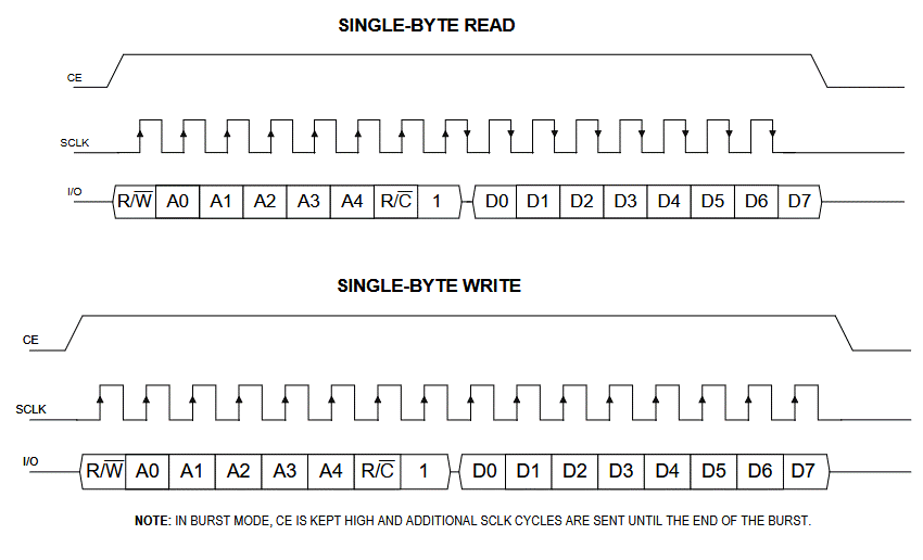
For a working system, however, the addition of the IDE board is advised as it allows connecting 2 SD cards, CF cards and upto 4 hard disks. All transactions can be done through either software IO or DMA. Since the 6809 is HALTed during the DMA operation (burst DMA) we can conduct transfers much faster than the 1 or 2MHz of the 6809 clocks (during DMA the E and Q clock continue as normal). The DMA controller uses a 16MHz clock (8Mbytes/s) such as to not exceed the speed of the CF cards that I have. The above shown logic analyser traces show the onset of a DMA read of a IDE device.
Extra serial ports are added through inclusion of a 4-port 6850 board that provides integrated serial to USB C converters with an option for mini USB.
No retro system is complete without a RAM disk and this system has one that is upto 4Mbytes large using a very small 4-byte memory interface using high-speed DMA transfers or programmed IO.
A video board with VGA output and USB keyboard & mouse is...
Read more »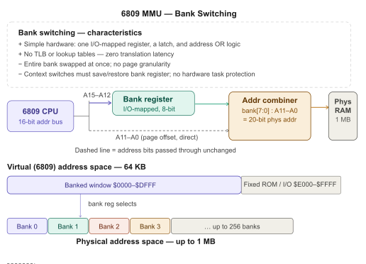
 6502Nerd
 Keith
Keith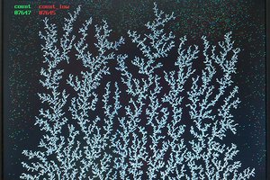
 Bruce Land
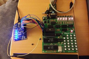
 Jac Goudsmit