roelof4
-
MMU design
2 days ago • 0 commentsThe presence of a Memory Management Unit is a requirement for multi-tasking operating system such as OS-9 and UniFLEX both of which have many features from UNIX.
Before diving into the details of the CS09 MMU I though it might be good to give an overview of the 3 main approaches to create extra address space (not necessarily MMU)
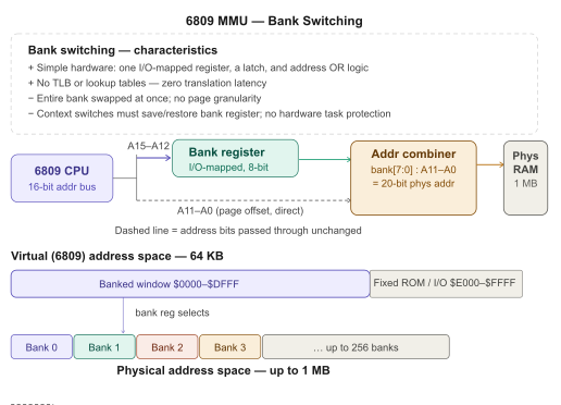
1. Bank switching:
![]()
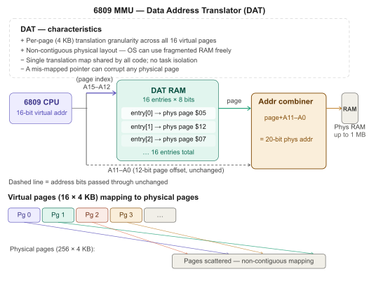
2. Data Address Translation:
![]()
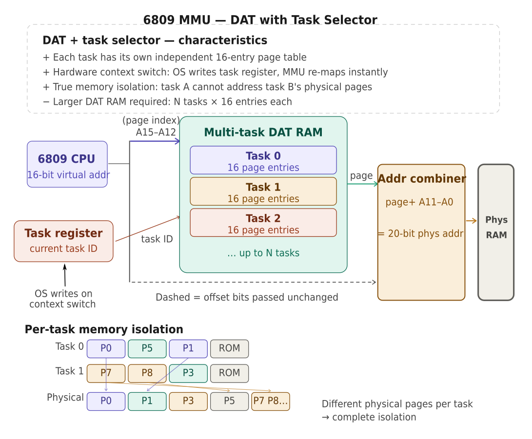
3. DAT + task selector:
![]()
The DAT + task selector gives most flexibility how to structure memory larger than 64kbyte and allows quick switching of the memory mapping of individual tasks without rewriting the DAT RAM.
Often the task register is a physical register (latch) in real implementations which the CPU will update when there is a switching of tasks. The CMS9639 took this concept one step further and introduced a small 4x8bit memory to replace the task register. This allowed 4 sets of task registers that would form:
- System task (task 0)
- User task
- DMA source task
- DMA destination task
Switching between these is automatic and done in the logic chip. So whenever a software or hardware interrupt occurs the System task will be selected and so on.
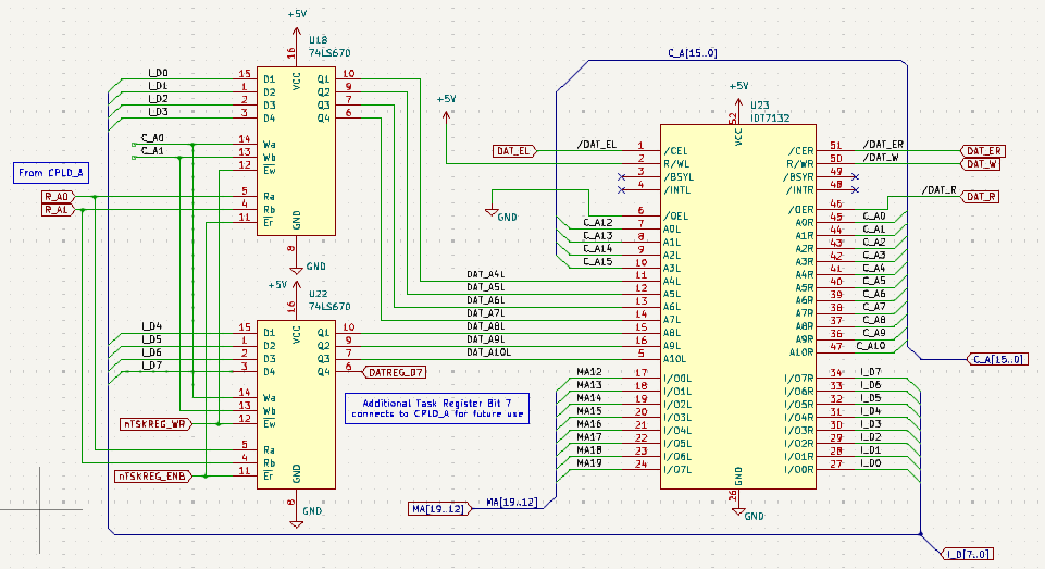
Below a snippet from the CS09 CPU schematic showing the chosen implementation:
![]()
Rather than using a standard 2kbyte RAM memory like the CMS9639, I have followed the approach by Kees Schoenmakers and used a dual-port memory chip (IDT7132). These are fast (35ns) and do away with extra tri-state buffers that are needed for normal memory when switching from MMU use to writing its contents. Here the righthand side of the dual-port memory provides access to its contents (I_D is the internal databus, C_A the CPU address bus). The left side takes CPU address lines A12..15 and the output from the small memory chips and outputs the MMU addresses MA12..MA19 which together with C_A0..11 will form the external address bus.
A set of pullup resistors on MA12..MA19 defines the external bus address before the dual-port RAM has its contents defined and taken out of tri-state. Currently the most significant bit (DATREG7) is not used and connected to the logic chip. In future this could be used to introduce memory write protection.
Motorola did, in fact, develop a MMU chip - the MC6829 - that provides 2kbyte pages. This chip was not long in production and not many copies are around. Unfortunately, the delay in outputting the translated address lines was significant which made operation at 2MHz next to impossible. I know only one commerical machine that used the MC6829, the Positron 9000 (https://binarydinosaurs.co.uk/Museum/Positron/).
-
Floppy Disk & Disk formatting
2 days ago • 0 commentsYou will have noticed that l have avoided the topic of disk formatting. Mainly because I did formatting of CF cards using the VCC simulator. Now that my system is about to be independent this topic needs to be tackled.
Other than floppy disks hard disk tend to come pre-formatted and the process is mainly writing key sectors with file system data. Typically this is called Logic formatting whereas floppy disks usually require physical and logical formatting. At the moment the driver can't do that and an upgrade is required. Here is some background info from the Microware System Programmer's Manual regarding the process of disk formatting.
Full detail in the Manual (pages 11-58..61 & 11-68..72). Various implementations of OS-9 have added further SS. parameters to the list. Here some details of interest:
As you may have noticed the IDEdrv (and all RBF drivers for that matter) have two useful routines accessible using the following system calls. At the moment these two routines are empty and just return to the caller. If we don't use physical formatting on the hard disk interface I don't expect we need to add anything. But for floppy disks it does require careful study. The actual number of different parameters for floppy disks is rather large with variations in track and sectors/track numbers, single/double sided, single/double density and 3 physical disk sizes.
Anyway, I am slowly entering the stage of preparing the floppy disk interface and will have to face doing the track formatting bit. I will start with the WD2797 controller which is fairly common and should be able to read all my old 5" disks.
The IDE interface has the same logic device as present on the CPU board and it features embedded RAM large enough to hold several sectors of data so I would like to structure the interface such that the CPU only has to give a read/write command to the WD2797 fill a buffer for writing, then go to sleep and let the logic chip collect/serve bytes from/to the on-chip RAM and generate an interrupt when the process is complete. That way the CPU is free to serve other tasks most efficiently.
Formatting disks
The
formatutility in the CMDS directory is not available in source form unfortunately. There is a commented disassembly file from the NitrOS9 community however, which is very helpful and helps with checking which SS. codes need implementation in the IDEdrv driver.The GetStt/SetStt routines are wildcard calls used to get or set a device's operating parameters. It may be necessary to examine or change the register stack which contains the values of MPU registers at the time of the
I$GetSttorI$SetSttservice request. The address of the register stack may be found inPD.RGS, located in the path descriptor.The calling convention is consistent across all SS. codes:
- Register A = Path number (the open path to the disk device, e.g.
/d0) - Register B = Function code (the SS. constant)
- Other registers depend on the specific function code
The SS. codes are defined in the OS9Defs equate file (part of the DEFS directory). They are passed in register B to both
I$GetStt(SWI2 +$8D) andI$SetStt(SWI2 +$8E).The Three Codes Used by
formatHere is a detailed breakdown of each of the three status codes:
SS.Reset— Controller Reset / Drive Restore- Code value:
$00 - Direction:
I$SetStt(SetStt — sends a command to the driver) - Purpose: Issues a hardware reset/restore to the disk controller. In the context of
format, this is used at the start to recalibrate the drive — stepping the head back to track 0. On floppy-based systems with the WD1793/1773 FDC chip, this causes a Restore command to be sent, which steps the head in until Track 0 is detected. - Registers in: A = path number, B =
SS.Reset($00) - Registers out: None meaningful (carry clear on success, set with error code in B on failure)
This is typically the very first hardware-level call
formatmakes, ensuring the drive is in a known state before writing begins.SS.WTrk— Write Track (Format a Track)- Code value:
$03 - Direction:
I$SetStt(SetStt) - Purpose: This is the most critical call for formatting. It instructs the RBF device driver to format a single track on the disk — writing the full track of sector headers (ID fields) and data fields in one disk revolution. This is the raw "write track" command that maps directly to the WD1793/1773 FDC's Write Track command.
- Registers in:
- A = path number
- B =
SS.WTrk($03) - X = address of the track format buffer (the byte stream to write, including ID address marks, sector ID fields, data address marks, and fill data)
- Y = length of the buffer
- Registers out: Carry clear on success
The
formatcommand builds the entire track image in memory — interleaved sectors, gap bytes, address marks, sector IDs — and hands the whole thing to the driver via this call. The driver passes it straight to the FDC's Write Track command. This is whyformatneeds to understand the disk geometry (sectors per track, interleave, side count, density) before making this call — it must construct the buffer correctly.On some implementations,
SS.DSizecan also be used as aSetSttto tell the driver what size to treat the disk as — useful when initialising a hard disk partition.How These Fit Together in
formatThe typical sequence
formatfollows using these calls is:- Open a path to the device (e.g.
/d0) in write mode SS.Reset— restore drive to track 0- For each track, build a track image buffer in memory (sector IDs, interleave, gap fills), then call
SS.WTrk(SetStt) to physically format that track - After all tracks are written, write the LSN 0 identification sector with all the
DD.*fields (total sectors, track size, allocation map size, etc.) and the allocation map at LSN 1 - Create the root directory at LSN 2 onwards
- Close the path
LSN 0 contains a description of the physical and logical characteristics of the disk. These characteristics are set by the
formatutility program when the disk is initialized. - Register A = Path number (the open path to the disk device, e.g.
-
Command line parameters OS-9
4 days ago • 0 commentsIn OS-9 for the 6809, command line parameters are passed to a program through a specific convention using the process's data area and registers at startup.
At Program Entry, the CPU Registers Contain:
- X — points to the start of the parameter string in memory
- Y — points to the top of the data area (the program's allocated memory)
- U — points to the bottom of the data area (start of the stack/data)
- D (A:B) — contains the size of the parameter string
The Parameter String
The parameter string is a raw text buffer containing everything typed after the command name on the shell line. For example, typing:
myprogram foo bar -x
...results in X pointing to
foo bar -x, with D holding its byte length.Key characteristics of the parameter string:
- It is not null-terminated — you must use the length in D to know where it ends
- It ends with a carriage return (0x0D), which counts as part of the string
- It may be empty (D = 1, pointing to just the CR) if no arguments were given
- The string lives in the system's I/O buffer area, not in your program's data area, so you should copy it if you need to keep it
Memory Layout at Entry
Low address
┌─────────────────────┐  ← U (data area base / stack bottom)
│   Program Stack     │
│         ↓           │
│    (grows down)     │
│                     │
│   Static Data       │
└─────────────────────┘  ← Y (top of data area)
High address

Separately, in system buffer:
┌─────────────────────┐  ← X
│  "foo bar -x\r"     │  (D bytes long)
└─────────────────────┘
Parsing Responsibility
OS-9 does no parsing for you. Unlike Unix which gives you
argc/argv, OS-9 hands you the raw string and leaves tokenization entirely to the program (or to a library like the one in the C runtime). You walk the string byte by byte, using the length in D as your bounds, splitting on spaces or other delimiters as needed.Standard I/O
At entry, the program's standard I/O paths are already open:
- Path 0 — standard input
- Path 1 — standard output
- Path 2 — standard error
These are inherited from the shell and ready to use via OS-9
I$Read/I$Writesystem calls.This convention is quite minimal and low-level compared to later systems, which is typical of OS-9's design philosophy of keeping the kernel small and fast on 8/16-bit hardware.
-
Realtime Clock
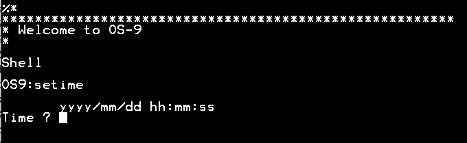
5 days ago • 0 commentsOS-9 uses a 100Hz oscillator driven signal to keep track of time. As mentioned this signal is connected through the PIA (MC68B21/HD63B21) and generates interrupts every 10ms. Upon calling the 'setime' command the PIA is initialised and valid time information becomes available to the system. Often the setime call is included in the 'startup' file which is automatically run at boot time.
![]()
Because there is a battery backed Realtime Clock (DS1302) available there is no need to manually enter date and time information (once the Realtime Clock is setup) every time the system boots.
In order to include the reading of the Realtime Clock at boot time changes are made to the Clock module and the setime command. Before discussing these changes it would be good to discuss the Realtime Clock itself and how it is interfaced to the CPU.
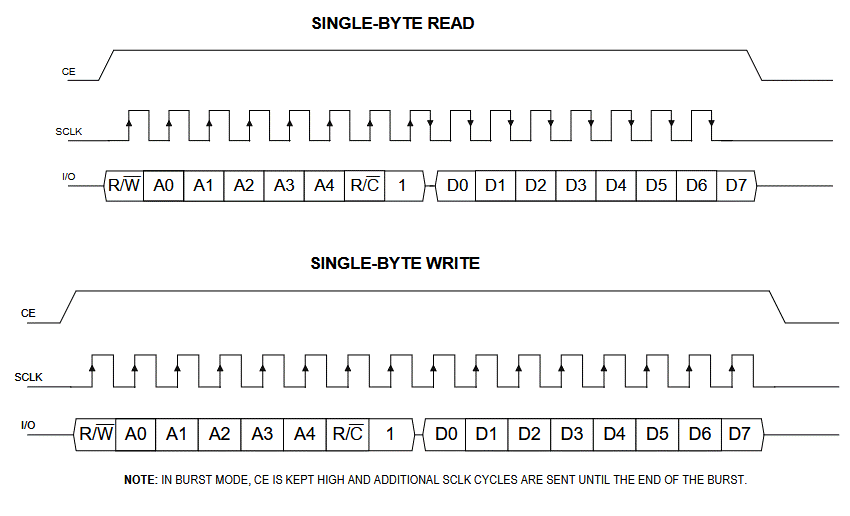
Unfortunately the use of the same Realtime clock chip (MSM5832) as used on the CMS9639 was not an option since this obsolete chip is difficult to source. Since there was little board space available it was decided to go for a chip with a small footprint and a serial interface. The DS1302 provides date, time and a small number of non-volatile RAM locations. Its interface is bespoke and shown below.
![]()
There are only three pins for exchanging data. A ChipEnable selects the device and data (IO) is shifted in/out using a SerialCLocK. Only the IO pin is bidirectional.
Originally I hooked the DS1302 to a couple of unused PIA lines and implemented a software interface to read/write date & time information. That resulted in quite a bit of code (provided) and since there was some space left over in the CPLD chip, it was decided to create a bespoke interface using a Verilog module.
For fun I tried to use one of the AI agents to write a module for me. This turned into a disappointing result that didn't work because the agent misinterpreted the asymmetry between reading & writing and was unable to generate the right code even when this issue was pointed out. After testing about ten versions I gave up :(
Thinking someone would have tackled this already I searched online and found a github repository (link in the code) that implemented burst reading/writing (many registers in one go without transmitting the address info for every register). I modified this code to include single register read/write which I needed to change the trickle charge settings. This code is provided in the file section. I will discuss the detailed instantiation of this module within the top level Verilog code in the near future. Since the actual code is rather large I will try to do this in sections.
From a software perspective this interface takes 8 memory locations ($FFB0..$FFB7) that provide date&time and command/status register ($FFB7). In the command register the user selects the type of operation (burst read/write or single register read/write). The status register shows when the serial interface is busy/ready with any operation.
With this interface tested it was decided to modify the 'year 2000 compliant version' (source available online: y2k upgrade) of the setime command (setime edition version 12) slightly to add an option (-s) to read the Realtime clock date & time information and copy this to the OS-9 time rather than typing it in. Setting of the Realtime Clock is done automatically if the 'setime' command is provided with user date&time information in the usual way (i.e. both OS-9 system time and Realtime Clock are set).
By adding 'setime -s' in the startup file the copying of the date&time info is automatic. The space between setime and -s is optional and 's' can be 'S'.
In the modified Clock module care is taken that the Realtime Clock is present and not in a 'halted' state before initialising.
At this point no use is made of the DS1302 RAM memory but the provided Verilog module and interface is fully prepared for it simply by reading/writing to different addresses within the DS1302 use can be made of these battery backed memory locations for storing data.
-
OS-9 DMA disk driver details 2
04/08/2026 at 09:52 • 0 commentsAs mentioned in the earlier log on the DMA disk driver, I have now written a RBF driver that sleeps during the phase after issuing a read/write command to the IDE disk controller and uses interrupts to wake up for the DMA transfer phase releasing the intervening time for other processes. There is no clash with other processes that want to use the DMA controller because it is only setup for data transfer during the actual data transfer phase, not when the IDE command is issued.
During the debugging I noticed an error stemming from the original driver (which is also updated) in that I tried to check the type of disk before it was defined... The verilog code for the IDE interface board was updated to provide the required interrupt signal and its associated status bit.
Both versions of this RBF driver are uploaded in source form.
Whilst going through the motions of updating the driver I noticed that the Programmer's Manual hints that since OS-9 level 2 version 1.2 (which is covered by the rev. H of the manual) a new SUSPEND state would improve the RBF even further since it does away with the wake up signalling ( section 5.3.2 page 5-11). For an electronic copy of the manual look at my CodeBerg repository under OS-9 documents.
So I have revised my IDE RBF driver using this new feature. So now there are three versions of the IDE RBF driver available. Obviously the latest: myIDEdrv_IRQ_Suspend.asm is the one to go for since it has all the features available that were discussed. The other two work and have been provided for those that would like to see the changes between them.
-
OS9 Clock Module
04/02/2026 at 12:00 • 0 commentsThe OS9 Clock module is an interesting one. In the OS9 hierachy diagram it sits together with Init at the same level as the OS9 kernel (OS9p1 & OS9p2).
The Clock module takes care of initialising the clock which is a 100Hz oscillator driven signal which, in our case, is connected to the onboard MC6821 (PIA). The PIA also provides a TimerEnable signal which is used to stop the 100Hz clock if it is logical '1'.
Also the Clock module provides seconds,minutes, hours, etc. registration based on the 'ticks' coming in from the 100Hz clock. This is done through generating interrupts by the PIA.
There is no direct start of the clock by the operating system. In fact the F$Time system call is only available when the Clock module is called using the Setime command which also starts the Clock.
Below a snippet showing how the PIA is setup and the clock is started by setting the TimerEnable signal low '0'. By default the TimerEnable is '1' due to a pullup resistor.
*****
*
*  CLOCK INITIALIZATION ENTRY
*
ClkEnt pshs cc
 lda #TickSec get ticks per second
 sta D.Tick
 lda #TickSec/10 set ticks/time slice
 sta D.TSlice
 sta D.Slice
 leax CLKSRV,pcr GET SERVICE ROUTINE
 stx D.IRQ SET INTERRUPT VECTOR

* PIA initialisation goes here
 ldx CLKPRT,pcr get PIA address
 orcc #IntMasks set interrupt masks
 clra
 sta 1,x clr control register
 lda #%00000001 PIA port A bit0 output, rest input
 sta ,x set data direction register
 lda #5 select pheripheral register & CRA1 interrupt enable, high to low
 sta 1,x set control register
 clra
 sta ,x clear bit 0 which enables 100Hz clock
 lda ,x clear any current interrupts

 puls cc restore interrupt masks
 leay TIMSVC,PCR
 OS9 F$SSvc SET TIME SERVICE ROUTINE

ClkEnt3 rts
Full Clock source code is attached.
Note: it is assumed that PIA A-side pins other than 'pin 0' are inputs. That is true (see schematic) for 'pin 4' or PA4 which is connected to the clock but not necessarily for the other pins. Currently these pins have no meaningfull purpose but one could consider using these and then the above PIA A-side initialisation needs to change.
-
CMS9639 specific changes OS9p1
04/02/2026 at 11:29 • 0 commentsThis first part of the OS-9 level 2 kernel (OS9p1) provides essential system calls that make up the operating system allowing proper task administration, memory management, etc.
Comparing the OS9p1 used for the CMS9639 with standard OS9p1 code it is clear that there are three low-level functions that have changed. All three are involved with moving data between tasks and in the case of the CMS9639 the memory-to-memory DMA facility is used even if there is only one byte to be moved.
Here, we don't consider changes in setting up/checking memory and the Data Address Translator (DAT, key part of the MMU) initialisation since these would be different for any system.
The changes are found in the code for Mover(00)/MoveRegs, PutRegs and STABX/LDABX (using source code labels). Below the difference between standard and CMS9639 is shown for PutRegs, which copies registers between tasks.
Below we compare PutRegs:
CMS9639:
************************************************************
*
* Subroutine PutRegs
*
* Copy User interrupt register stack
*
* Input: X = Process Descriptor ptr
* U = local stack ptr
*
* Output: none
*
* Data: none
*
* Calls: uses DMA to copy register stack
*
PutRegs ldb P$Task,X get process task
 andb #^SysTask
 clra
 pshs u,x,cc
 ldx P$SP,X get process stack ptr
 exg x,u switch source & destination
PutReg.A equ *
 orcc #IntMasks
 sta >Tsk.Src Task to copy from
 stx >$FFC0 DMAC source address register
 stu >$FFC4 DMAC destination address register
 ldx #R$Size
 stx >$FFC2 DMAC Source byte count register
 stx >$FFC6 DMAC Destination byte count register
 stb >Tsk.Dst Task to copy to
 ldb #$03
 stb >ContrlSW send command
 nop
 puls pc,u,x,cc
Standard:
************************************************************
*
*     Subroutine PutRegs
*
*   Copy User interrupt register stack
*
* Input: X = Process Descriptor ptr
*        U = local stack ptr
*
* Output: none
*
* Data: none
*
* Calls: MoveRegs
*
PutRegs ldb P$Task,x get process task
 lda D.SysTsk get system stack
 pshs u,y,x,DP,D,CC save registers
 ldx P$SP,x get process stack ptr
 exg x,u switch source & destination
PutReg.A equ *
 ldy #R$Size/2 get double byte count
 tfr B,DP copy process task
 orcc #IntMasks set interrupt masks
 lbra MoveRegs
Mover10 lda 1,s get source task number
 orcc #IntMasks set interrupt masks
MoveRegs sta DAT.Task set source task
 ldd ,x++ get data double byte
 exg b,dp switch data & task
 stb DAT.Task
 exg b,dp switch back
 std ,u++
Mover30 lda #SysTask get system task
 sta DAT.Task set system task
 lda 0,s get previous masks
 tfr a,cc reset interrupt masks
 leay -1,y count double byte
 bne Mover10 branch if more
 puls pc,u,y,x,dp,d,cc
The DMA version essentially uploads source and destination information and moves bytes during DMA just after 3 is written to the ControlSwitch (ARM DMA). Task switching is automatic between source and destination.
For the standard case there is changing of task needed for every (double)byte. R$Size is the number of bytes to move.
Apart from the data moving routines there is one further CMS9639 specific change that is at the heart of system calls. System calls use a SWI2 software interrupt followed by a PostByte which indicates what system call is to be performed. Normally software collects the PostByte from user space and increments the program counter to skip the PostByte upon return. The CMS9639 has a dedicated circuit that captures the PostByte and places it in memory location $FFFA0. It also increments the program counter before placing it on the stack.
In the snippet from OS9p1 this process can be found in detail for both cases using conditional assembly:
************************************************************
*
* System Service Request Routine
*
* Process system service requests
*
* Input: S = value of stack after interrupt
*
* Output: none
*
* Data: D.SysDis, D.SysPrc
*
* Calls: Dispatch, SysRet
*
SysSvc leau 0,s get registers ptr
 ifeq CPUType-CMS9639
 ldb Postbyte get service code
 lda R$CC,u get caller's interrupt masks
 tfr a,cc restore interrupt masks
 else
 lda R$CC,u get caller's interrupt masks
 tfr a,cc restore interrupt masks
 ldx R$PC,u get program counter
 ldb ,x+ get service code
 stx R$PC,u update program counter
 endc
 ldy D.SysDis get system dispatch table ptr
 bsr Dispatch dispatch to service routine
 lbra SysRet
-
RAM disk
03/29/2026 at 15:37 • 0 commentsWith available (and affordable) memory quickly passing the 64kbyte mark many people employed extra RAM in their system during the 1980s in order to create quick access disk storage. Within OS-9 it is very simple to define extra drives with bespoke drivers to integrate these into the operating system.
Often the access would be memory mapped access through a window of varying size with 1-4kbytes as a common option. Using bank switching this window would cover the full extent of the available RAM disk size.
I have designed the RAM disk for the CS09 system in a different way because I would like to keep the number of memory locations for I/O to a minimum. This method is much like normal disk access via a dedicated controller. There are only four bytes mapped into the CPU's address space through which all data transfer happens. Besides a data register there are 2 registers (16-bits) that set the Logical Sector Number of the sector to be accessed and a further command/status register. That's it.
Internally, the RAM disk logic has an 8-bit counter which auto increments whenever a read or write to the data register is performed. Together with the 16-bit LSN there is room for 2^24 bytes (16Mbyte) on the RAM disk. There is an option for using a 9-bit internal counter for use with UniFLEX which uses sectors of 512-bytes.
Access to the disk would require uploading of the LSN number of the sector followed by 256 reads/writes from/to the data register. The internal 8-bit counter get cleared automatically after any change of the LSN registers. Through the command register the disk can be write-protected.
Using one of the two DMA engines on the CPU board all data transfers are really fast.
RAM disk memory is low-power CMOS and the memory chips have backup batteries so that the RAM disk contents is non-volatile.
-
Floppy disk controllers
03/27/2026 at 12:35 • 0 commentsDuring the 1980's the Western Digital floppy controllers were abundant. Starting with the 179x series and 279x ones after that. There were also more compact solutions like the 177x series which were popular due to the low supporting chip count. Like many I used all of these and learned to live with them. Especially the requirement to not poll their status too quickly was a nuisance.
With that in mind I made two different designs of the IDE interface. One with a WD2793 and one with a newer WD37C65 device. The latter one is a NEC uP765 like interface plus some extra support so that it is a one chip solution. Both should allow reading of both 8" and 5.25" disks but the WD37C65 goes further (3" extra density) so an interesting option to explore. A 3D KiCAD representation of the WD37C65 version is uploaded to the picture gallery.
I have an old Siemens 8" drive which is well preserved and some original TSC FLEX OS 8" floppies (!) and it will be fun to see if I can read these eventually.
OS-9 drivers for the WD279x are around and should be easy to adapt. However, for a multi-tasking system these can be a drag since byte don't come out as a stream of bytes that can be transferred as a burst DMA. Instead people have used 'cycle stealing' DMA something which requires some overhead in managing.
So during design time I thought of a way to buffer the bytes from/to floppy drives sector by sector. Hence by keeping a 256-byte buffer between the CPU and the floppy drive, the sequence of writing/reading to/from floppy drives becomes much like interfacing to IDE disks and we can employ burst DMA transfer of data.
There is still the issue of how to deal with disk formatting which requires more than 256-bytes but it should be simple to create a bypass to the sector buffer and handle these the 'old way'.
-
OS-9 DMA disk driver details
03/26/2026 at 10:37 • 0 commentsAs mentioned I use an IDE (PATA) type interface to connect to storage devices like hard disks or Compact Flash cards. There are several adapters for CompactFlash cards that plug into IDE connectors to make that easy.
Currently the Boot loader module that resides in EPROM reads the disk using Programmed Input/Ouput or in other words data is transferred not using DMA but simply by programmatically reading byte for byte. This allows the code to be very compact and since that is the only task running has little downside.
The IDEdrv RBF driver is using DMA to quickly load sectors of data to memory. Since we are using burst DMA (during which the processor is HALTed) no other task is running. However, there is a significant delay between issuing a read sector by DMA command and the onset of the DMA transfer. The delay depends on the drive used. For the CompactFlash card that I use (Scandisk Ultra II) this delay is 0.28ms much longer than the actual DMA transfer of 256bytes (which is several tens of microseconds). Currently the driver simply polls the DataReady bit during these 0.28ms then the CPU is HALTed once data is ready. So no interrupts are involved at this stage.
It would be better to issue the read sector command go to sleep so other tasks can run and use an interrupt when done. But it is a bit more complicated than that. Because the DMA controller needs to be setup before the transfer we can't do this at the time of issuing the read sector command. That is because the same DMA controller is used for other tasks (such as moving data between tasks by OS-9 system calls). So one would have to issue the sector read command without setting up the DMA registers, go to sleep and wake up when data is ready as signalled by the IDE disk. Then load the DMA registers and acknowledge the DMA transfer. That way there is no clash between DMA users and other tasks can use the 0.28ms of waiting for data from the disk for useful operations.
Although IDE devices have a dedicated Interrupt request line, this line is toggled only at the end of the DMA transfer which is not what we want because the driver will release the CPU directly after the DMA transfer. In our case we would like an interrupt signal directly before the IDE disk is ready to do the DMA transfer so we can quickly upload the DMA registers and allow the transfer to happen. Plan is to use the DMA request signal to trigger the interrupt request and toggle the DMA acknowledge line to the IDE disk once the DMA registers are loaded and the DMA is armed. Just like the CPU board, the IDE interface is built around a complex logic circuit and details of signalling can be adjusted easily through changes in the verilog code.
Details of putting read/write disk to sleep and how to wake them up are described in the OS-9 programmers manual (pages 6-15 and 6-16) and the interrupt service routine on page 6-19. I have revision H (January 1984) of the manual.
I had a look around to see how legacy drivers handle this and unfortuately I haven't found many such disk drivers around. There is the GIMIX G68 driver but that is centred on doing 'cycle stealing' DMA as far as I can see. It does show how the Sleep and Busy and Wakeup signalling is done. It also introduces a system variable that indicates if the DMA device is 'in use' or 'free'.
For those interested in the code I have attached the source code for the Boot module and the current IDEdrv RBF device driver (still working out how to setup the CodeBerg repository ...).
6809/6309 Eurocard CPU System
A retrosystem based on the elegant 8/16 bit 6809 processor capable of running UniFLEX and OS9 level II multiuser/multitasking OS