Robert Gawron
Design Philosophy
Silicon Photomultiplier vs Traditional PMT
Conventional gamma spectrometers commonly use vacuum photomultiplier tubes (PMTs). These require high-voltage supplies in the kilovolt range, are mechanically fragile, and are sensitive to magnetic fields.
In this project, a Silicon Photomultiplier (SiPM) is used instead. The SiPM operates at significantly lower bias voltage (tens of volts rather than kilovolts), is mechanically robust, compact, and insensitive to magnetic fields. These characteristics simplify the power supply design and mechanical integration.
Digital vs Analog Processing
Traditional spectrometers implement CR-RC shaping networks and peak detection entirely in analog hardware. This approach is cost-effective but offers limited flexibility, as parameter changes require hardware modification.
In this system, pulse shaping and peak detection are performed digitally after high-speed sampling. This increases flexibility and allows signal processing parameters to be modified in firmware without hardware changes. The trade-off is higher performance requirements for the ADC and the need for an FPGA rather than a microcontroller, which increases overall system cost.
Hardware
Architecture Overview
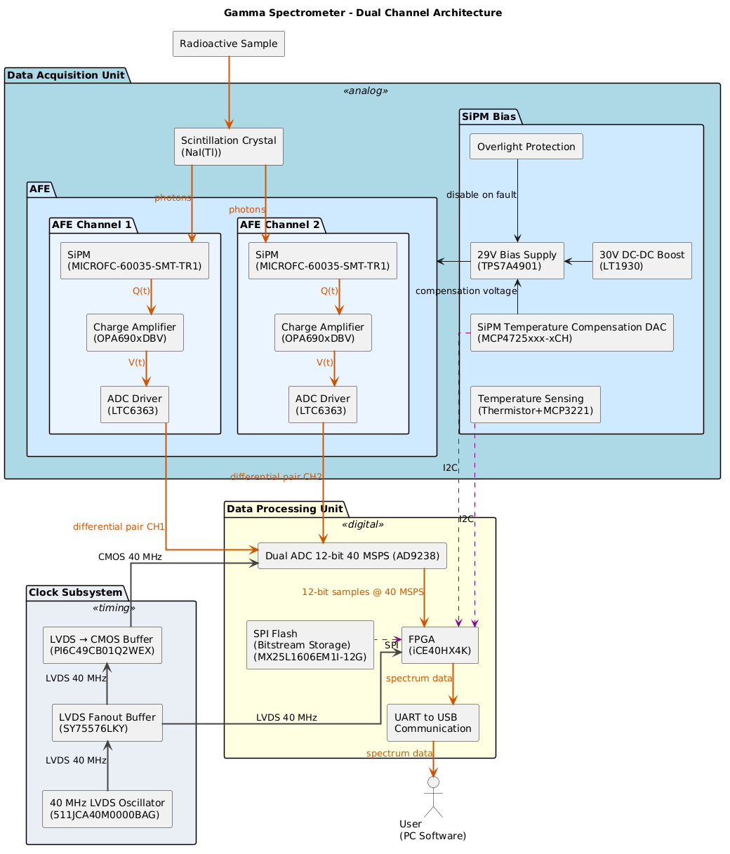
The hardware consists of four main parts:
Analog Processing
Handles low-level currents produced by the sensor (typically 1uA - 1mA pulses, 10mV - 1V after amplification):
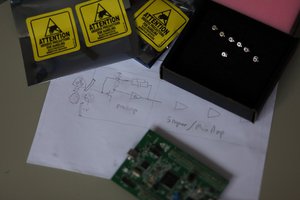
- NaI(Tl) Scintillator Crystal - Converts gamma rays into visible light pulses through scintillation
- Silicon Photomultiplier: MICROFC-60035-SMT-TR1 SiPM - Converts light pulses from the scintillator crystal into electrical current pulses
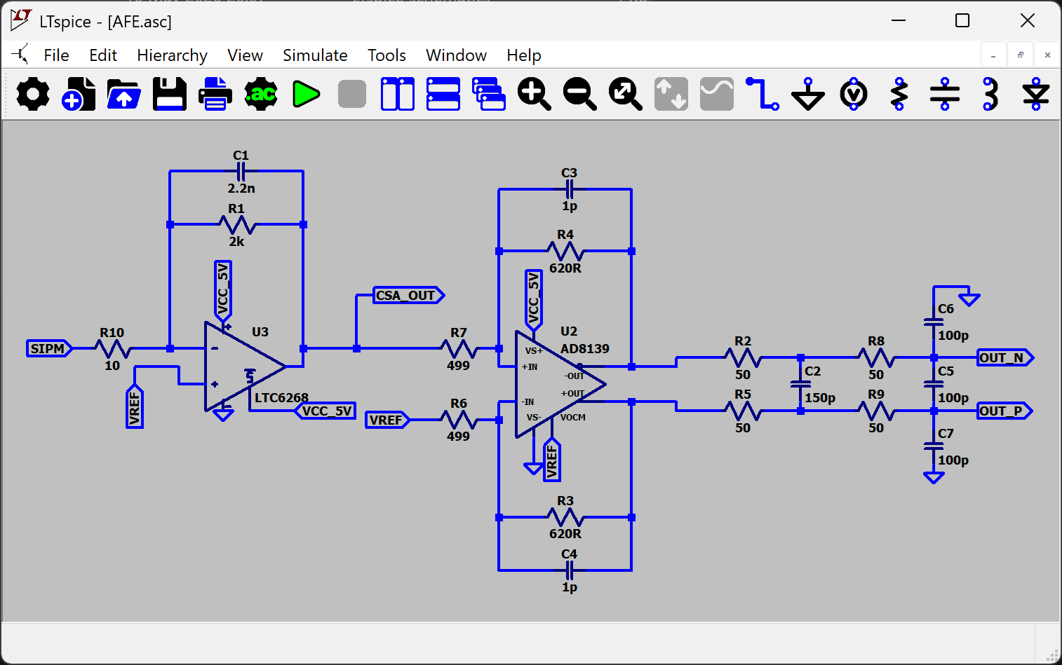
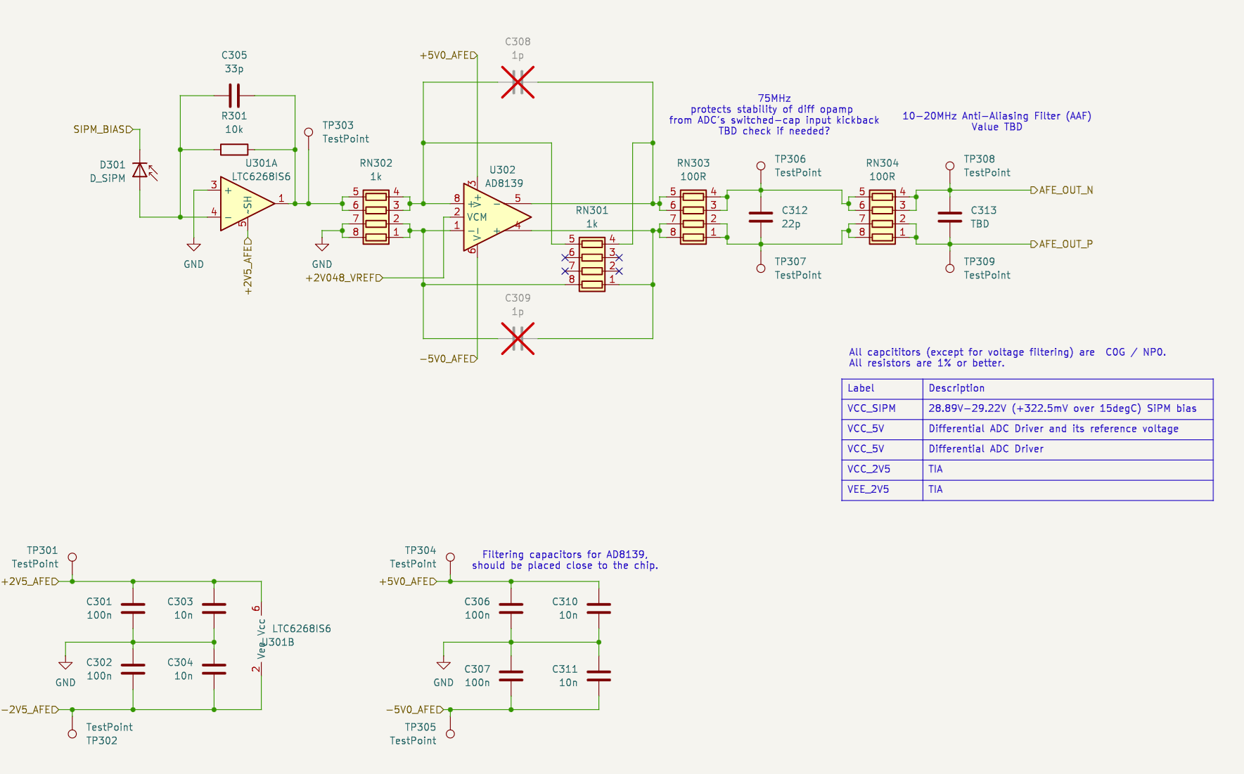
- Amplifier: OPA690 - can be configured either as a charge amplifier or as a transimpedance amplifier (TIA), depending on the selected feedback network. In the current design, the amplifier is configured as a charge amplifier.
- Charge Amplifier Configuration. In this mode, the amplifier integrates the input current pulse generated by the SiPM and converts the total collected charge into a proportional output voltage. The output voltage is defined by the feedback capacitor:
This can also be expressed as:
Where:
The total charge generated by the Silicon Photomultiplier (SiPM).
The feedback capacitance of the integrator or transimpedance stage.
The time-dependent input current pulse from the detector.
- Transimpedance Amplifier (TIA) Configuration. In this configuration, the output voltage is proportional to instantaneous input current:
Where:
The feedback resistor that determines the gain of the transimpedance stage.
The instantaneous input current flowing from the sensor into the amplifier.
- Charge Amplifier Configuration. In this mode, the amplifier integrates the input current pulse generated by the SiPM and converts the total collected charge into a proportional output voltage. The output voltage is defined by the feedback capacitor:
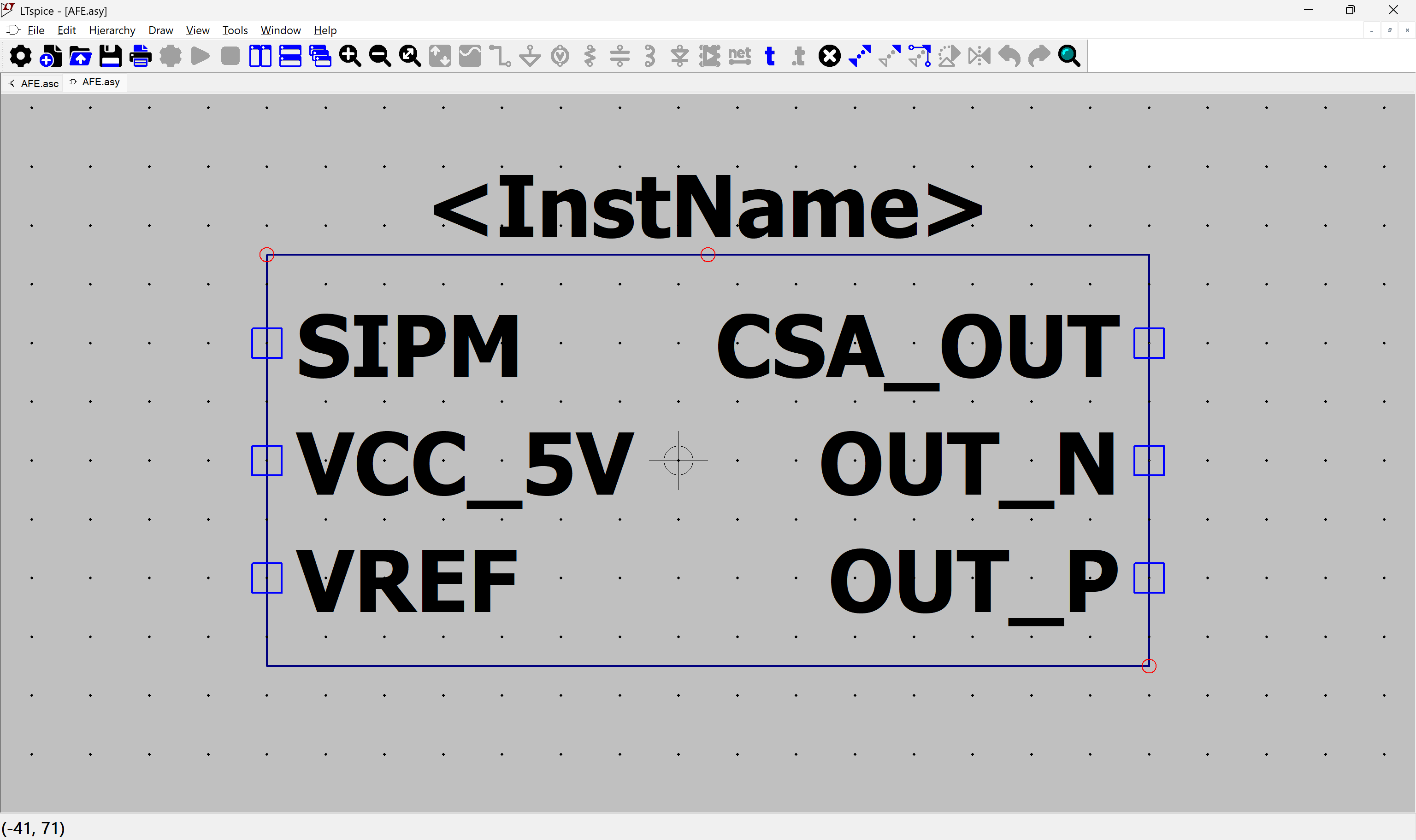
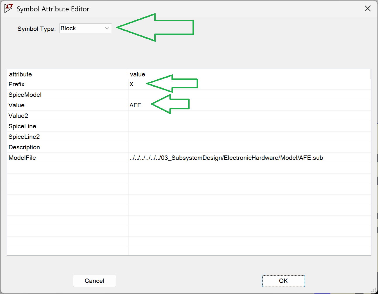
- Differential ADC Driver: AD8139 - Converts the single-ended amplifier output into a differential signal suitable for the ADC input. It also sets the required common-mode voltage (1.5 V) needed by ADC.
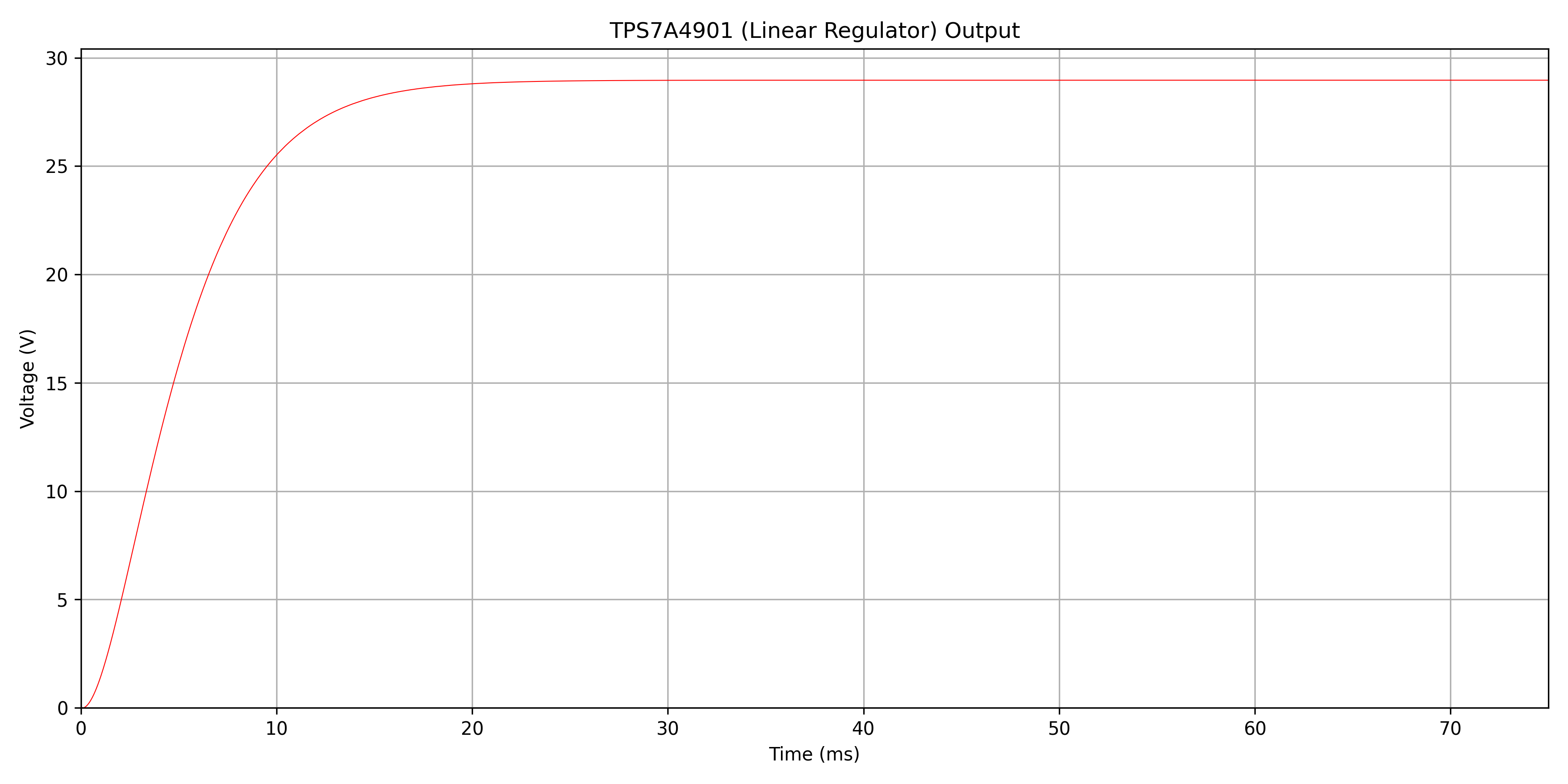
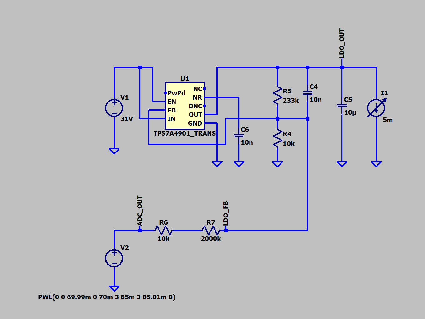
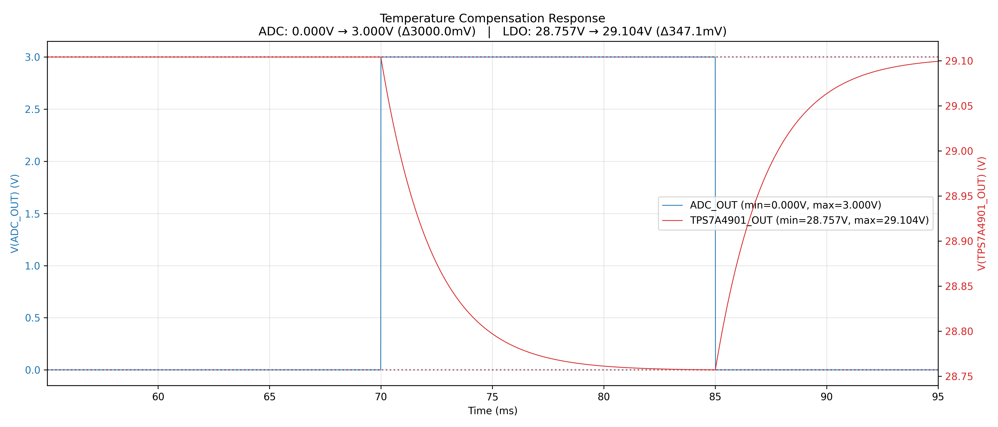
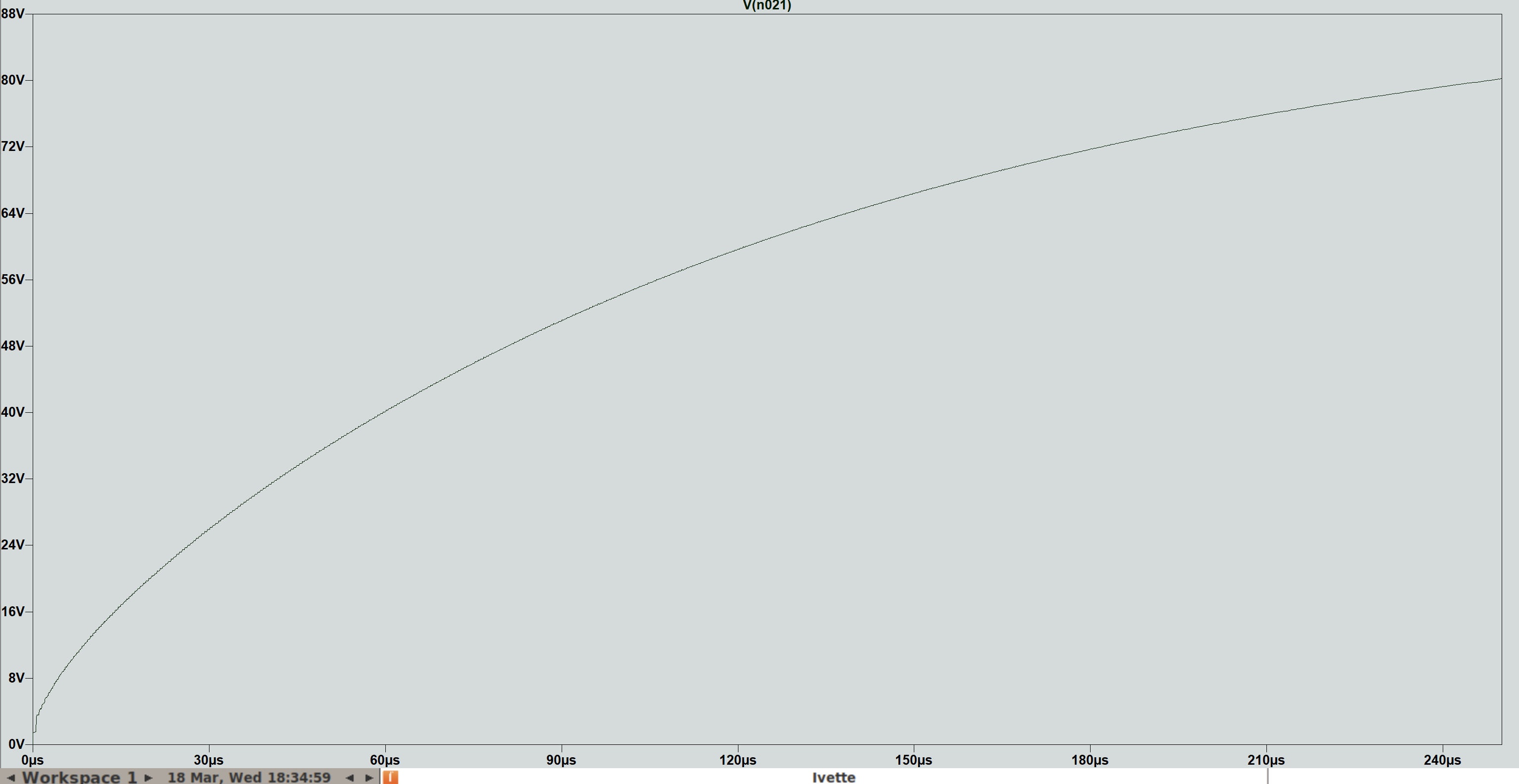
- Bias Supply - Provides a stable and filtered 29 V bias voltage for the SiPM. The bias voltage is adjustable to compensate for temperature-dependent gain variation of the SiPM.
Note: Analog pulse shaping and peak detection are not used - raw signal is digitized directly and processed in FPGA.
Digital processing
Performs high-speed sampling and real-time pulse analysis:
- ADC: AD9238 - 2-channel, 12-bit, 40 MSPS sampling rate. ch channel produces 480 Mbps (60 MB/s), resulting in 960 Mbps (120 MB/s) total sample data rate.
- FPGA: iCE40HX4K - Real-time digital pulse processing (trapezoidal filtering, peak detection, histogram generation)
- SPI Flash: MX25L1606EM1I-12G - Stores FPGA configuration bitstream
- SPI Port - External header for FPGA programming
- UART to USB Converter: CH340X - Communication interface to PC.
Clock Subsystem
to be refined
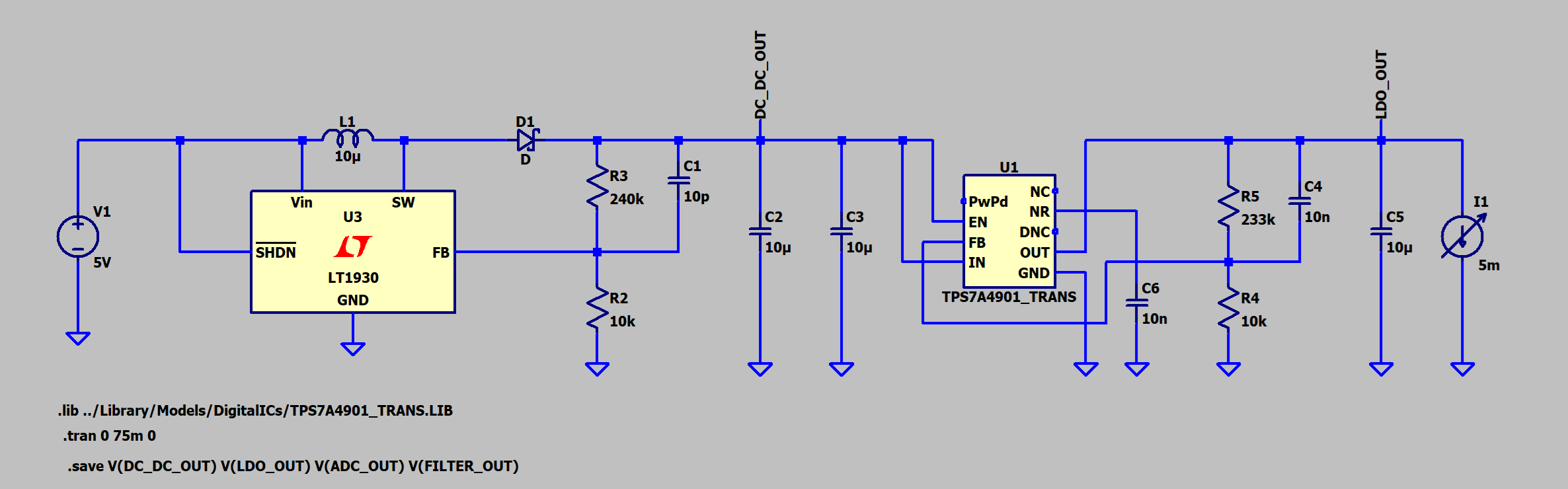
Power Distribution
to be refined
Tools: KiCad.
Software
The project is developed using a completely open-source FPGA toolchain. The RTL code is written in VHDL-2008, synthesized with Yosys + GHDL, and targets...
Read more »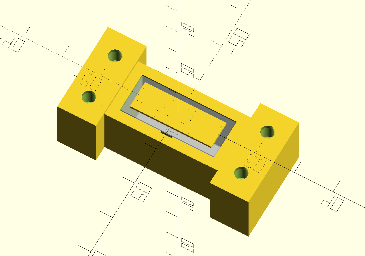
 Jithin
 Christoph Tack
 mihai.cuciuc