Robert Gawron
-
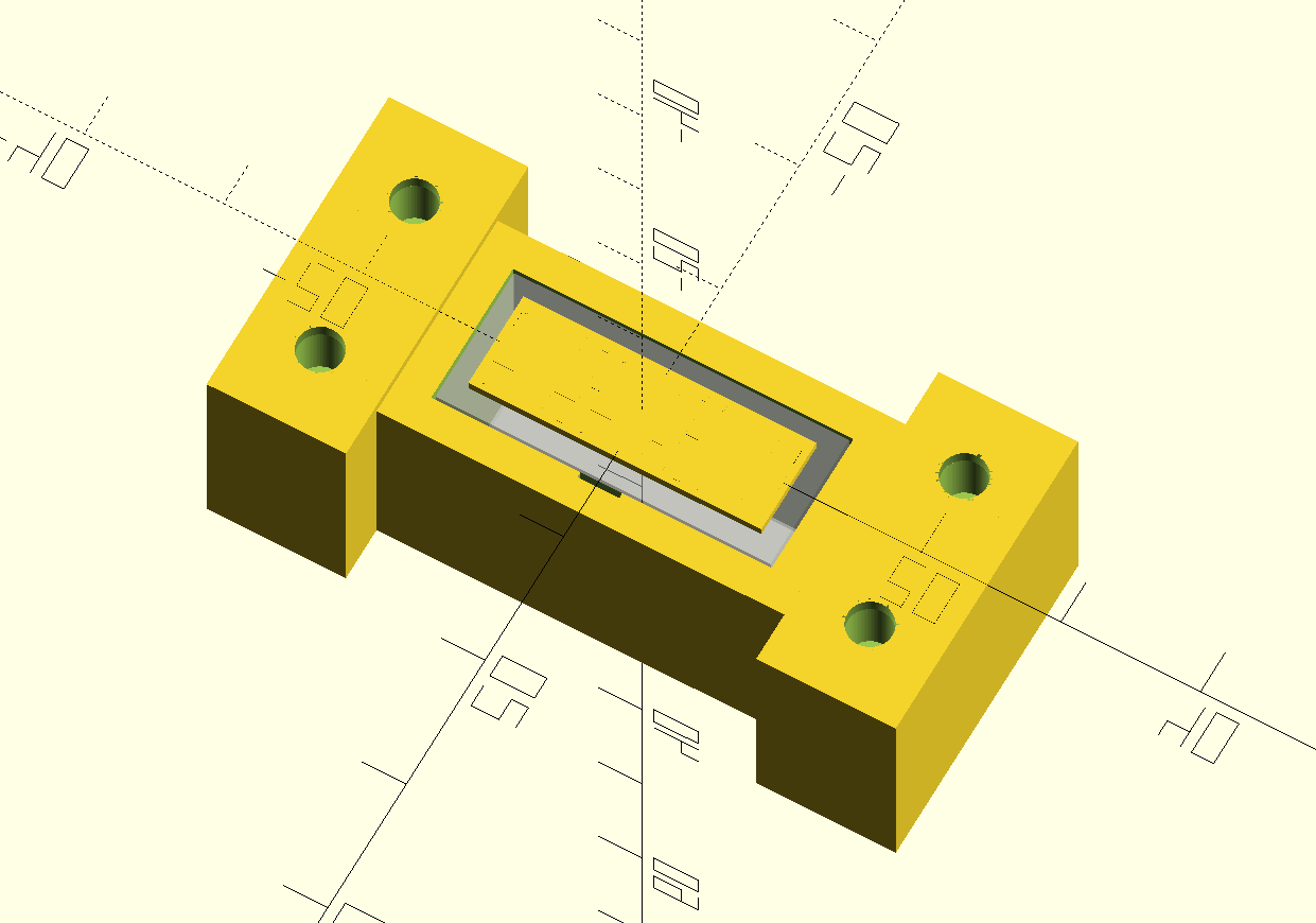
New scintillator selection, light reflections, mechanical setup using OpenSCAD
05/25/2026 at 09:16 • 0 commentsI've bought the scintillation crystal, however not the NaI(Tl) one as planned but LYSO (Lutetium Yttrium Orthosilicate). The thing is, NaI(Tl) with shipment is 180 euros, and the LYSO (8 pieces) is 124 euros with shipment, so it's much cheaper. This has some implications:
- The LYSO I've bought is not a single crystal but 8 of them, so I will need to use some optical gel to optically connect them.
- The crystal is naturally radioactive so it messes a bit with readings. On the other hand, it can be said that this natural peak is like a self-calibration (that can be done later in the software). So it's both positive and negative.
- The crystal is not hygroscopic and doesn't need a fabric envelope, so it's a small advantage.
- The peak emission wavelength of the NaI(Tl) and LYSO is the same and is matched with the SiPM, so it's ok.
![]()
The thing is that to maximize light absorption by the SiPM, the crystal should be covered (except the SiPM area because that would block the light) with reflective material. I've added space in the holder for that. At first, I was thinking that the best thing would be some kind of mirror or polished metal. That's what I think upon hearing "reflection" :)
Actually not. To avoid bouncing in circles, it's better to use something porous as a reflective material, ideally PTFE (which is just a sheet of Teflon). It's white. This is the one I plan to buy (1mm thickness).
I still haven't found a shop that sells optical gel. Surprisingly, it seems like it's not available on AliExpress.
-
Reusable, testable blocks in LTspice
05/14/2026 at 17:13 • 0 commentsI'm testing the model of my analog frontend against requirements in LTspice, and in this post, I will share an LTspice hack I came up with for the problems below:
- There are many configuration analysis models in LTspice that I need. If I kept everything in one file, I would need to comment/uncomment what I need for each simulation. This is annoying.
- Depending on the tests, I need different models of the SiPM. Again, I could connect/disconnect what I need, but this is annoying and error-prone.
- If I split these into different LTspice simulations and then change the analog frontend (for example, a resistor value), I need to manually update every single file to keep them coherent.
The solution is to create a symbol for the part under test (the analog frontend) and reuse it in all my LTspice test benches. Since the symbol lives in two files (.asy and .sub), they just need to be regenerated from the main analog frontend model, and then all test models can use them.
It looks simple and reasonable, but it didn't work well in LTspice at first..
I made the tutorial below for myself and others on how to do it
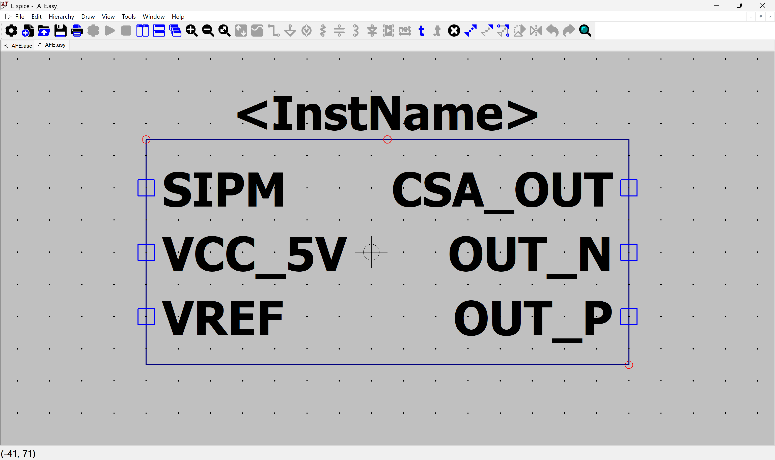
Step 1: pure model (.asc file)
We create the model of the component under test (as an .asc file) without:
- Any power sources
- Any sensors
- Any LTspice directives
Just a pure circuit with no external components.
Add labels to its inputs, outputs, and power nodes (GND doesn't need one). Anything that needs to be connected in the test bench models must be labeled; otherwise, those nets won't be visible in the subcircuit.
![]()
Step 2: symbol of the model (.asy file)
Now we create the .asy file (representing how the component looks on the schematic and defining its pin names and numbers):
Click "Hierarchy" -> "Create a New Symbol from this Schematic", and click Yes.
Now we have our symbol. Note that it is filled with a background color (grey).![]()
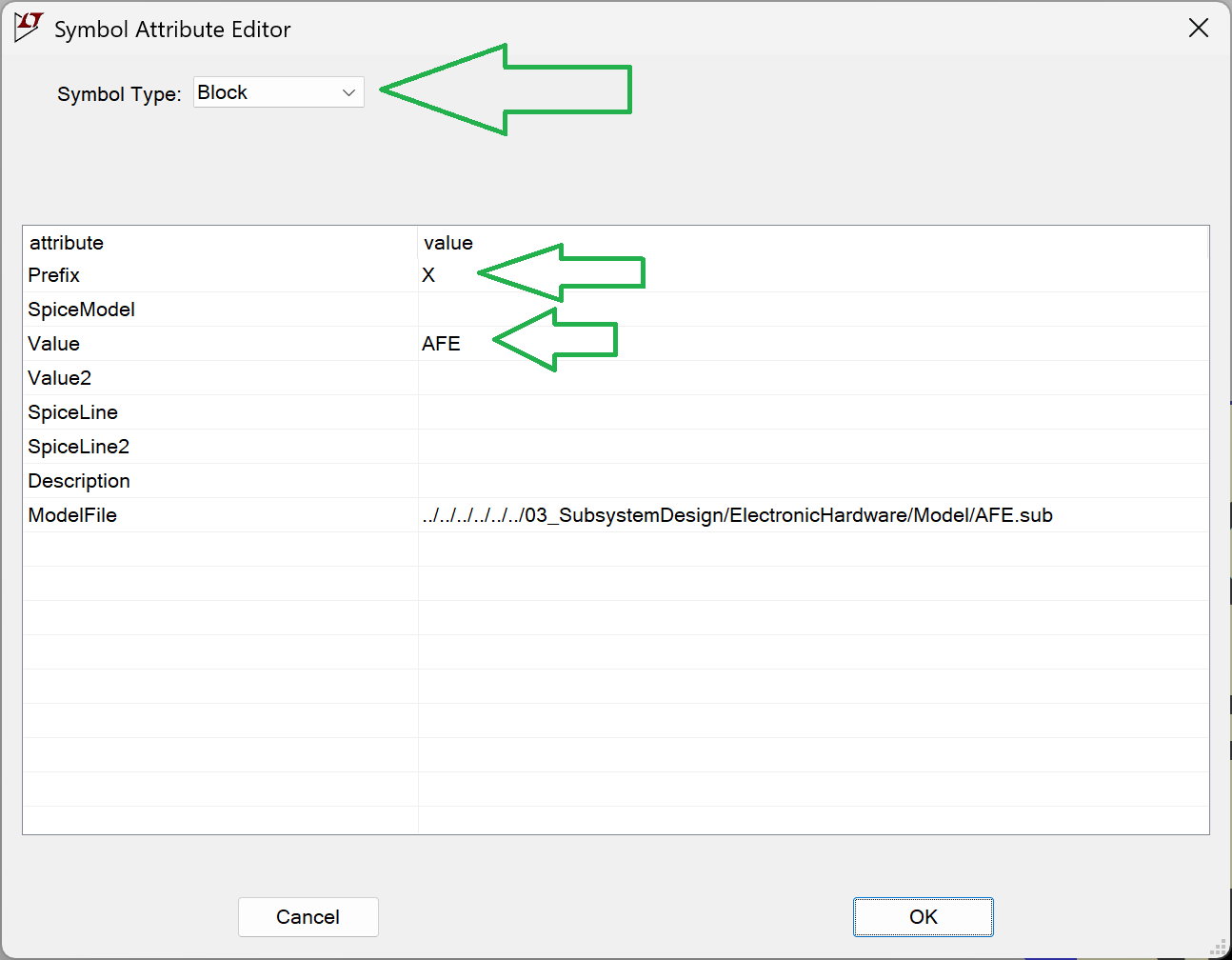
Go to "Attributes" -> "Edit Attributes".
The Prefix must be "X". This is important because it tells LTspice to treat the component as a subcircuit (otherwise, it won't work).
.asy file of the tested model should be in the same folder as its .asc file.![]()
Step 3: behavioural model (.sub file)
We need a .sub file (which describes how the circuit behaves, this is the real model). The automatic generation never worked well for me, so I made a workaround.
Open the .asy file in a text editor and find the entries like these:
SYMATTR Value AFE

...

PINATTR PinName SIPM
PINATTR SpiceOrder 1
PIN -112 -32 LEFT 8
PINATTR PinName VCC_5V
PINATTR SpiceOrder 2
PIN -112 0 LEFT 8
PINATTR PinName VREF
We are interested in the names found after PinName, they will be different depending on what is on the model (for me they are as above).
Next, create the unpopulated .sub file. The subcircuit file for the tested model should be in the same folder as the .asc and .asy files. They should all have the same filename, differing only by their extensions.
Using a text editor, place the following dummy content into the .sub file:
.SUBCKT AFE SIPM VCC_5V VREF CSA_OUT OUT_N OUT_P
** CIRCUIT_BODY_START **
** CIRCUIT_BODY_END **
.ENDS AFE
The line starting with .SUBCKT is important, based on your specific model:
- First element: This is the name of your model (this must match the SYMATTR Value from the .asy file).
- Then goes the PINS, list the pins exactly as they appeared in the .asy file (PINATTR PinName). The order matters!
Place the Python script in the same folder as your files and run it.
import re
from pathlib import Path


def extract_net_body(net_path: Path) -> str:
    """
    Extract all lines from .net except .end (case insensitive).
    """
    lines = net_path.read_text(encoding="utf-8").splitlines()

    filtered = []
    for line in lines:
        stripped = line.strip().lower()
        if stripped == ".end":
            continue
        filtered.append(line)

    return "\n".join(filtered)


def replace_subckt_body(sub_path: Path, new_body: str) -> None:
    """
    Replace content between CIRCUIT_BODY_START and CIRCUIT_BODY_END
    with new_body.
    """

    content = sub_path.read_text(encoding="utf-8")

    pattern = re.compile(
        r"(\*\* CIRCUIT_BODY_START \*\*).*?(\*\* CIRCUIT_BODY_END \*\*)",
        re.DOTALL
    )

    replacement = (
        "** CIRCUIT_BODY_START **\n\n"
        + new_body.strip()
        + "\n\n** CIRCUIT_BODY_END **"
    )

    # Use lambda to prevent re.sub from interpreting backslashes
    new_content = re.sub(pattern, lambda m: replacement, content)

    sub_path.write_text(new_content, encoding="utf-8")

def net_to_sub(net_file, sub_file):
    net_path = Path(net_file)
    sub_path = Path(sub_file)

    if not net_path.exists():
        raise FileNotFoundError(f".net file not found: {net_file}")
    if not sub_path.exists():
        raise FileNotFoundError(f".sub file not found: {sub_file}")

    print("Extracting .net body...")
    net_body = extract_net_body(net_path)

    print("Updating .sub file...")
    replace_subckt_body(sub_path, net_body)

    print("Subcircuit updated successfully.")


# =============================
# Example usage
# =============================
if __name__ == "__main__":
    net_to_sub(
        r"AFE.net",
        r"AFE.sub"
    )
Now we have both the .asy and .sub files. As long as there is no change to the pins (which shouldn't happen often), we only need to run "View" -> "Spice Netlist" and launch the Python script whenever you modify the circuit. All your test bench models will now automatically use the updated version of the tested model.
Step 4: How to use the component in other models
This part is a bit messy: the .asy file needs to be copied into the same folder as the test bench models (I haven't found a way to reference it via a relative path yet).
However, the .sub file can be referenced using an LTspice directive:
spice
.include "../path_to_file/AFE.sub"
Here is how it looks in practice:
![]()
Link to where it is on Github:
-
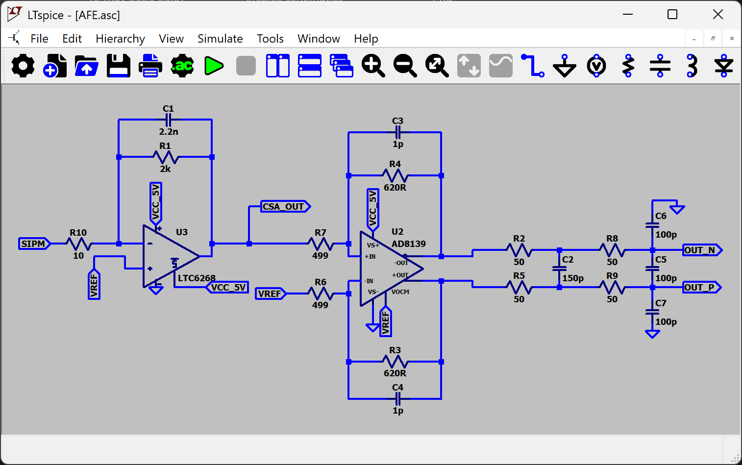
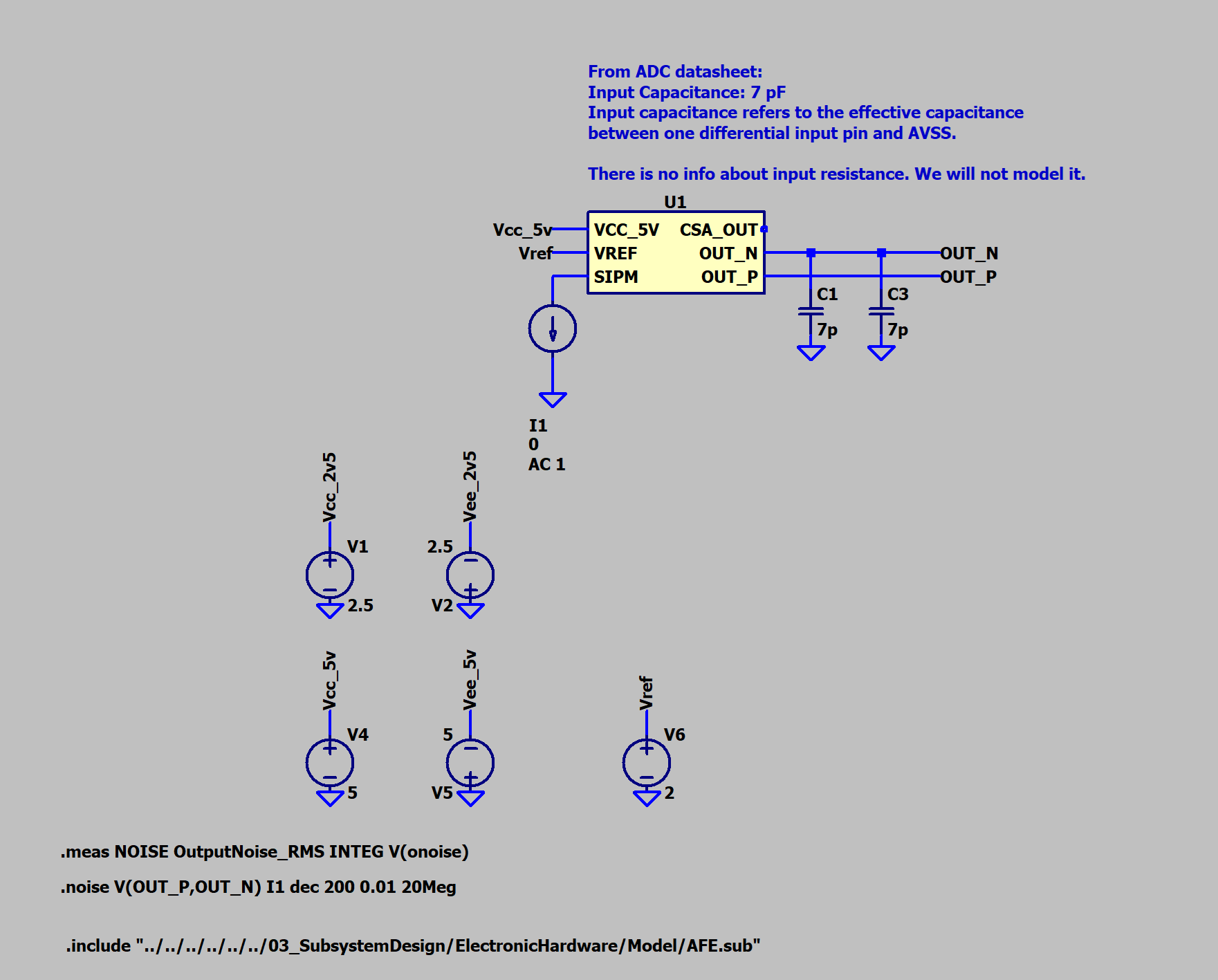
SiPM internal capacitance, transimpedance and charge amplifiers
04/18/2026 at 15:46 • 0 commentsThere has been a lot going on with the project lately :)
The SiPM sensor I originally planned to use (MICROFC-60035-SMT-TR1) has 3.4nF internal capacitance, which is huge. Normally, to compensate for this in a transimpedance amplifier (TIA), a capacitor is connected between the inverting input and the output. Since the capacitance is so large, the circuit will effectively behave more like a charge amplifier rather than a true transimpedance amplifier.
I think this may be a problem because a charge amplifier, by its nature, integrates the input signal. If we simplify the math: integrals are slow, derivatives are fast. There are gamma spectrometers with charge amplifier as first stage so the design is not wrong however. The pulses will be slower and wider, so the device will have lower time resolution. In that case, using a fast ADC and FPGA might be overkill, also fast ADC are expensive.
My idea is to switch from the AD9226 (65 MSPS, single channel) to the AD9238 (pin-compatible variants: 20/40/65 MSPS, dual channel). I plan to use the 40 MSPS version for now and switch to a higher sampling rate later if needed. This already saves roughly 20 euros.
Since the ADC has two channels, I could use two smaller SiPMs (3×3 mm) with two analog front-ends. Two channels require twice as many op-amps, so the savings form choosing different ADC are eaten, but I still think this is a better solution because:
- The sensor capacitance is roughly x5 lower.
- Having two channels gives the opportunity to perform some digital processing in the FPGA (I don’t have idea about digital processing yet, but I will look into it later).
The downside is that the total sensor area will be twice smaller: 6x6 mm vs. two 3x3 mm sensors.
In the image below, you can see how one channel currently looks. It includes a TIA and a differential amplifier. Due to the ADC change, the element values will change, but the general idea will remain the same I think.
![]()
-
Try to keep it easy to solder and cheap
03/25/2026 at 22:34 • 0 commentsI think it's best to handle all the math is in the FPGA (but I don't know FPGA). That way, no need for a peak detector or RC circuits, and it’s a lot easier to fix code than it is to reroute a PCB. Also I've tried to choose easy to solder chips:
- MICROFC-60035-SMT-TR1 as a sensor
- LTC6268 as transimpedance amplifier
- LTC6363 differential amplifier
- AD9226 fast "and good?" ADC
- iCE40HX4K + SPI flash for data handling
- maybe some STM32 for communicating with outside world
TBD:
- SW tools for iCE40HX4K
- divide project on what can be done in v1 vs what can be touched in v1, learned and finalized later.
-
LTspice+JupyterNotebook simulation of sensor biasing
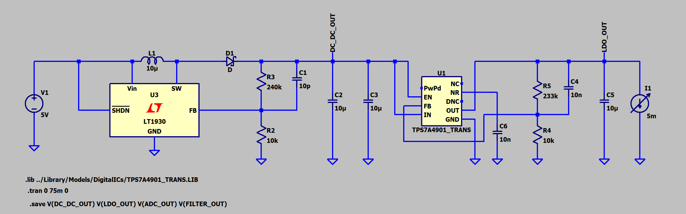
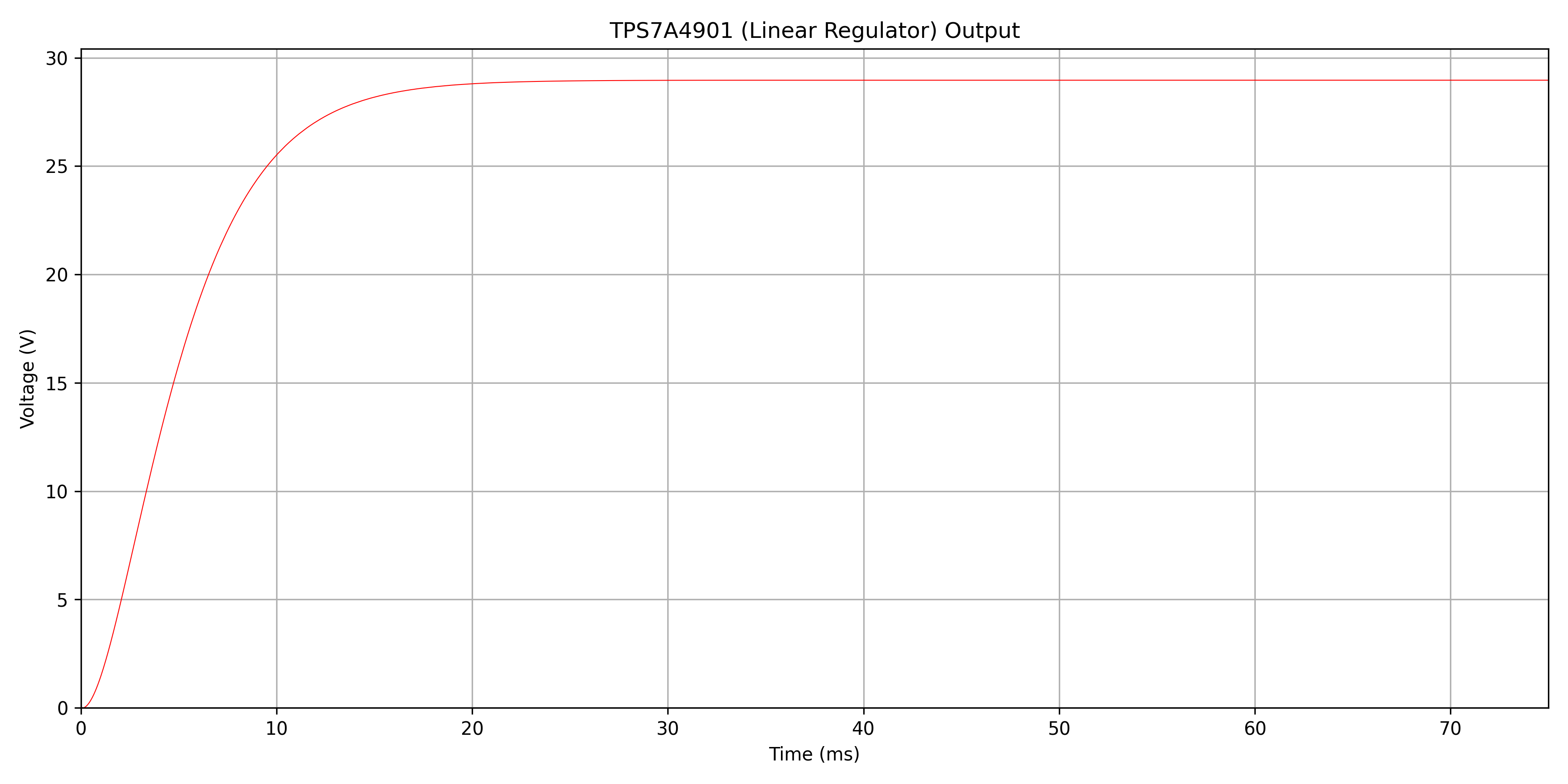
03/21/2026 at 18:15 • 0 commentsMost important, there's a relatively cheap photomultiplier diode, looks perfect for this project: MICROFC-60035-SMT-TR1.
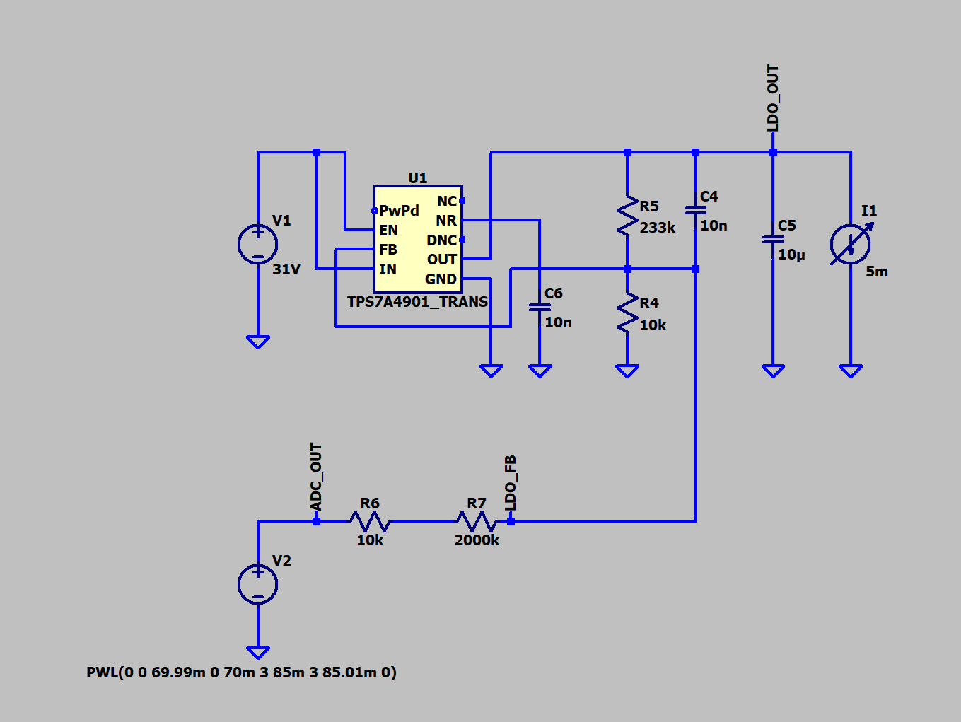
I've decided to change plans and use a regular DC/DC converter plus a silent voltage regulator at the output; this way, the output voltage will be well-stabilized and can be adjusted for temperature changes.
If I made the math right, mentioned above diode needs a bias of 28.89V - 29.22V (why it's not constant later on in post) assuming the device will work in temperature range of 20C-35C (meaning 15C span)?
I've made this simulation and it seems to work (but it's just a simulation):
![]()
![]()
The silicon photomultiplier (SiPM) requires not only a stable bias voltage, but also temperature-dependent voltage adjustment. This is necessary to compensate for the parameter called "temperature dependence of Vbr" (breakdown voltage), specified in mV/°C. As the SiPM temperature increases, its breakdown voltage shifts, causing its detection characteristics to change. To maintain consistent meassurements, the bias voltage must be increased proportionally - by the specified mV/°C value for each degree of temperature rise.
The TPS7A4901DGNR regulator uses a feedback (FB) pin to monitor its output via a resistor divider. By injecting additional voltage into this node, we trick the regulator into sensing a higher-than-actual output, causing it to reduce the real output voltage. This provides a mechanism for precise voltage adjustment through an external control signal directly from microcontroller or via DAC for better precision.
I didn't simulate gathering the actual temperature, as this seems easy.
![]()
![]()
The diagrams were made in LTspice, and then raw output files were parsed in Jupyter Notebook Python to produce the above diagrams; this way, the diagrams look much better, and it's possible to do extra math.
Jupyter Notebook is a web server that acts as a nice wrapper for small scripts, etc.; it's not a full IDE, but it works great for small snippets of code. It's containerized and launched inside Docker, but the web port is exposed so that on the host it can be accessed via a web browser.
-
Choosing a Scintillator crystal, PIN photodiode, and its biasing
03/18/2026 at 19:08 • 0 commentsChoosing detector elements
This project will be much more expensive than what I was thinking - scintillator crystals and PIN diodes are expensive! I've found a shop online that has scintillator crystals, and it seems to me that this one will be good:
- Sodium-doped cesium iodide crystal (CsI(Na)), 10x10x10mm .. $290.00 + tax + probably duty because they are in China and I'm in Europe. EDIT: just use cheapest NaTI that is sealed (because it's hygroscopic) https://www.epic-scintillator.com/NaI-crystal-scintillator/NaI-crystal-30x24mm?sort=p.price&order=ASC or maybe use cheapest plastic one to check if device works and then switch to better ones: https://www.epic-scintillator.com/Plastic-scintillator?product_id=912&sort=p.price&order=ASC EDIT2: this site is cheaper: https://www.ost-photonics.com/product/diameter-1-inch-x-1-inch-naitl-scintillator/
- S3590-08 PIN photodiode .. 111 euro + tax. EDIT: this is better/cheapper: https://eu.mouser.com/ProductDetail/onsemi/MICROFC-60035-SMT-TR1?qs=byeeYqUIh0MxSRIaBcfS6g%3D%3D or https://eu.mouser.com/ProductDetail/ams-OSRAM/SFH-2240-A01?qs=T%252BzbugeAwjjFSBEKp8QF2A%3D%3D choose scintillator first, it's usable shape wavelength peak will dictate sensor choose.
Hopefully, the frontend is the most pricey part, I think.
Choosing sensor biasing
The PIN diode can be biased either negatively (pulses will be positive, meaning signal peaks when a particle is detected will be higher than the background) or positively (peaks will be lower). Negative biasing seems better, so I will stick to it.
The S3590-08 can withstand 100V of reverse voltage, so I plan to bias it with -70V - that should be good enough and it gives margins (I want to be extra safe since it costs money!).
The easiest and cleanest way, at least for a prototype, is to just use 12V batteries in series. I've already used this when I was building a semiconductor radioactivity detector (which is a much more simplified version of the gamma spectrometer being designed here). The problem with batteries is that they lose voltage over time (although the PIN diode takes almost no current) and they take up a lot of space on the PCB/device.
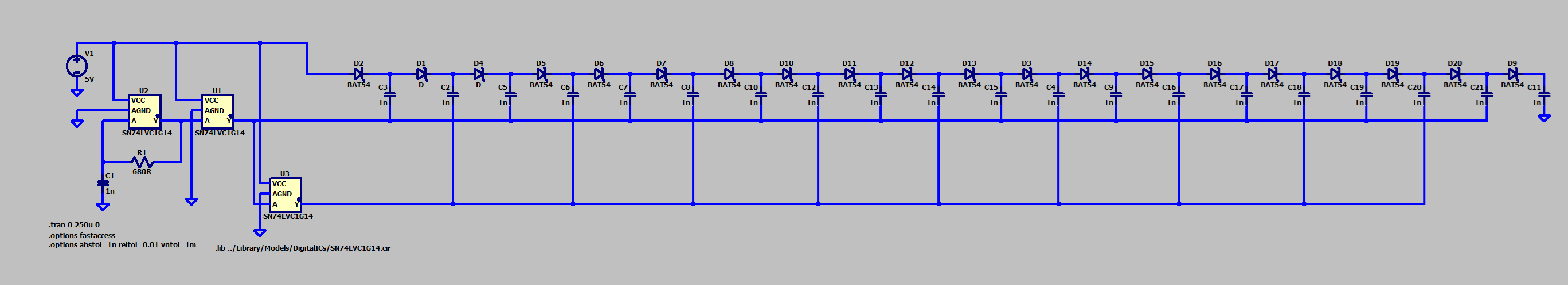
I was thinking about a DC/DC converter to produce the needed -70V, but then I would need a coil or a transformer in it, and I don't want to mess up the small signal from the diode with EMI interference from a coil. Maybe that's not a problem at all; I don't know, as I haven't built such a thing before.
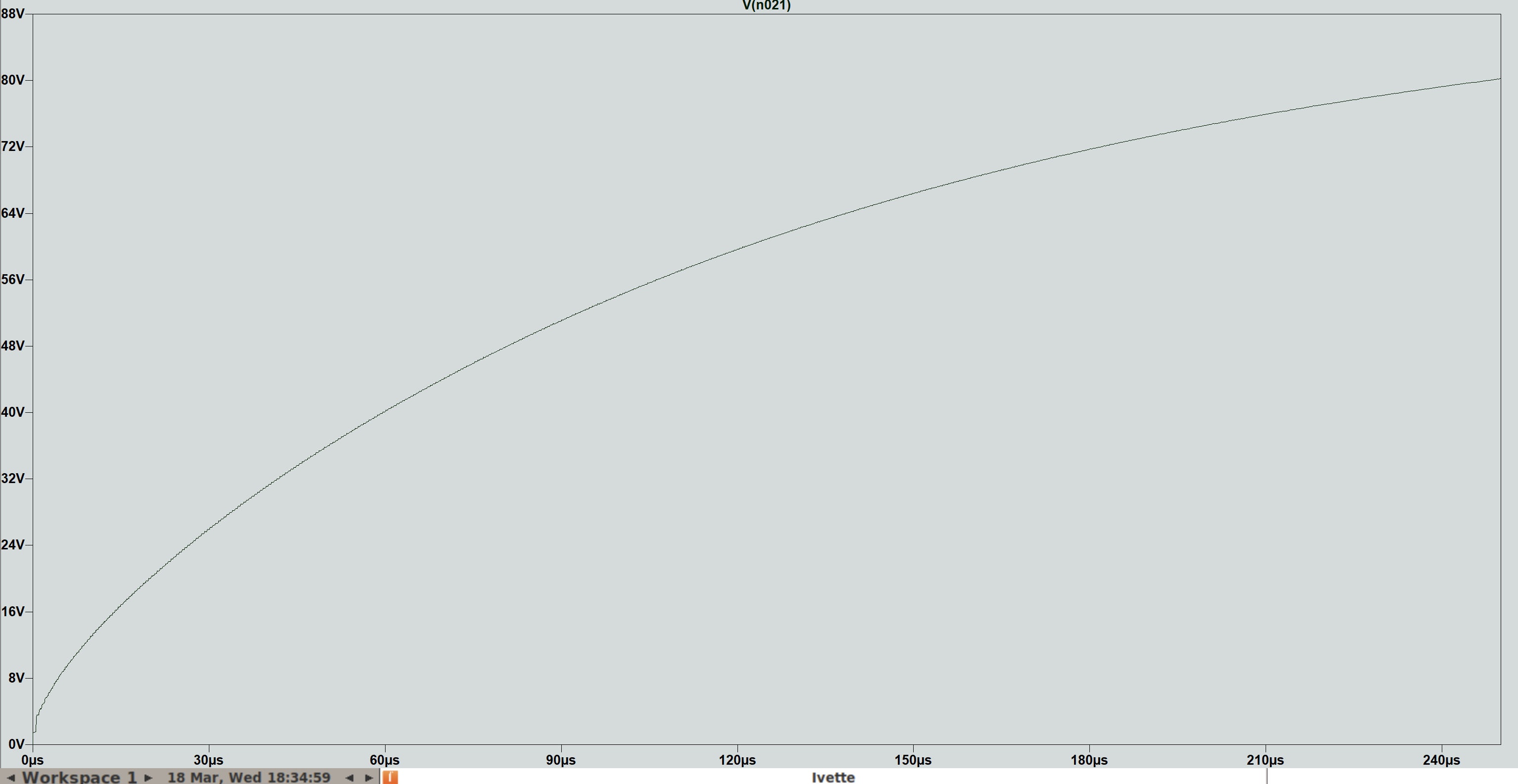
I then moved toward a voltage multiplier and designed a Dickson charge pump using LTspice, which at least in theory would give me the needed -70V from a usual 5V. Here is the circuit and simulation:
![]()
![]()
Will this circuit work in real conditions with all the parasitic capacitances, resistances, etc? I don't know, so I will put space on the PCB for both batteries in series and this charge pump. If the pump works, great, if not, I will use batteries in the first prototype.
Silicon Photomultiplier Gamma Spectrometer
Gamma spectrometer using scintillation crystal, Silicon Photomultiplier (SiPM), and all-digital FPGA signal processing