Before diving into the hardware, a quick note for those unfamiliar with the platform. Meshtastic is an open-source, off-grid, decentralized mesh network that runs on low-cost LoRa radios. Devices automatically rebroadcast messages they receive, extending range hop by hop — no cell towers, no internet, no infrastructure required. The network supports up to 100 nodes concurrently, and each node can optionally share its GPS position with the rest of the mesh. The record for a single hop is 254 km. It is a practical tool for hiking groups, emergency communication, and any scenario where you need reliable off-grid messaging.
The natural question when you have a DevPocket in your pocket is: can it become a Meshtastic node? The answer is yes — with a dedicated mPCIe module.
Module Overview
The Meshtastic mPCIe module adds two things to DevPocket: a LoRa radio for mesh communication and a GNSS receiver for GPS position reporting. Both are well-proven, compact components that fit within the mPCIe full-size form factor.
(Screenshot: Meshtastic mPCIe module(TOP))
(Screenshot: Meshtastic mPCIe module(BOT))
RF Side — HT-RA62 (SX1262)
The LoRa radio is the Heltec HT-RA62 — a stamp-hole module built around the Semtech SX1262 chip. Key specs:
Parameter
Value
Chipset
SX1262
Frequency
863–928 MHz (868 MHz EU / 915 MHz US)
Max TX power
+22 dBm
Receive sensitivity
down to –139 dBm
Interface
SPI
Dimensions
16 × 17 × 0.8 mm
The SX1262 communicates with the ESP32 via SPI (SCK, MOSI, MISO, NSS) with additional control lines: TXEN, RXEN for TX/RX switching, BUSY for ready signalling, and DIO1 for interrupt-driven packet reception. The antenna port is an IPEX MHF1 coaxial connector (J2, 208890-0001) with a small matching network (L6 6.8nH, C10/C14 8.2pF) on the RF output.
(Screenshot: schematic HT-RA62)
GPS Side — u-blox MAX-M8Q + MAX2659 LNA
The GNSS receiver is the u-blox MAX-M8Q — a compact chip-size module (9.7 × 10.1 mm) with a TCXO for improved cold-start performance. It supports concurrent reception of GPS, GLONASS, Galileo, and BeiDou with a navigation sensitivity of –167 dBm and a horizontal position accuracy of 2.5m CEP.
Parameter
Value
Engine
u-blox M8
GNSS systems
GPS, GLONASS, Galileo, BeiDou (3 concurrent)
Navigation sensitivity
–167 dBm
Position accuracy
2.5 m CEP
Update rate
up to 10 Hz (GPS + GLONASS)
Interface
UART + I2C
Supply voltage
2.7–3.6V
The MAX-M8Q connects to the ESP32 via UART1 (TXD/RXD) and also exposes an I2C interface (SDA/SCL via R1/R2 0Ω solder-select jumpers). A TIMEPULSE output is available for precise timing applications.
To improve sensitivity with a passive antenna, the module includes a Maxim MAX2659ELT+ GPS LNA. The LNA sits between the antenna connector (J1, coaxial) and the MAX-M8Q RF input, and is controlled by the LNA_EN signal from the ESP32. The matching network on the LNA input uses L4 (6.8nH) and C14 (8.2pF) for 1575 MHz GPS band impedance matching.
(Screenshot: schematic u-blox MAX-M8Q)
Firmware
DevPocket with this module runs the standard Meshtastic firmware for ESP32. The SX1262 and u-blox M8 are both well-supported by the Meshtastic firmware stack out of the box. The device pairs with the Meshtastic Android or iOS app over Bluetooth, and GPS position is automatically reported to the mesh.
The module schematic and KiCad project files are published on GitHub alongside the rest of the DevPocket design files.
The first real-world testing of DevPocket — connecting to a phone, running scripts, testing the sensor module — worked well functionally. But that is exactly when schematic mistakes surface: not during simulation, not during layout review, but when you actually use the thing. Below is a full breakdown of every issue found in Rev.1 and how each one was fixed in Rev.2.
Fix 1 — Wrong LDO for a Battery-Powered Device
Rev.1: The 3.3V rail was regulated by an AMS1117-3.3. It is a widely used part, but it has a high quiescent current and performs poorly at micro-load — which is exactly the operating condition of a device that spends most of its life in deep sleep. Every unnecessary microamp of idle current directly eats into battery life.
Rev.2: Replaced with AP2112K-3.3 — a true LDO with a very low quiescent current, well-suited for light and intermittent loads. For a battery device this is not a minor detail: a difference of even 100 µA in sleep mode translates to hours of lost standby time.
(Schematic screenshot: Power sheet — AMS1117 → AP2112K change)
Fix 2 — No Way to Cut Peripheral Power in Sleep
Rev.1: Peripheral power rails were always active. The core problem: WS2812B and CP2102GM have no hardware sleep mode and no other way to reduce their consumption. Left powered, they draw enough current to significantly shorten battery life even when the ESP32 itself is in deep sleep.
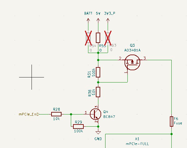
Rev.2: A new control signal Peripheral_En driven by an ESP32 GPIO was added. It switches a P-channel MOSFET (AO3401A) that cuts power to the WS2812B chain, the CP2102GM bridge, and the mPCIe slot simultaneously. Before entering deep sleep, the firmware pulls Peripheral_En to disable all peripherals — the device now actually sleeps rather than just having the MCU idle while everything else keeps running.
(Schematic screenshot: Power sheet — AO3401A peripheral switch)
Fix 3 — No Battery Voltage Monitoring
Rev.1: Battery voltage was not measured anywhere in the design. There was no way to display a charge level indicator or implement low-battery protection in firmware.
Rev.2: A resistor voltage divider was added from the BATT rail to an ESP32 ADC input, exposed as the BATT_ADC signal. The divider scales the LiPo voltage range (3.0–4.2V) into the ESP32's ADC input range. Firmware can now track battery state and warn the user via the OLED or LEDs.
(Schematic screenshot: Digital sheet — BATT_ADC divider)
Fix 4 — No Test Points and Unreliable Reset
Rev.1: There were no test points on critical signals. The practical consequence: to flash MicroPython for the first time you need to hold GPIO0 low during boot to enter download mode — without a test point this is fiddly and unreliable on a compact board.
Rev.2: Test points TP1–TP3 were added on key signals including GPIO0, making the initial flashing procedure straightforward. Additionally, STM6519AHARUB6F was added as a dedicated reset supervisor — a "smart reset button". Holding the reset button for an extended period forces a guaranteed hardware reset of the MCU. This matters in practice: if a script hangs and stops responding, a software reset won't help. You need the iron guarantee.
(Schematic screenshot: Digital sheet — TP1–TP3 and STM6519)
Fix 5 — No Pull-Up Resistors on CHIP_EN and GPIO0
Rev.1: The CHIP_EN and GPIO0 lines had no pull-up resistors. ESP32 requires CHIP_EN to be held high for normal operation, and GPIO0 must be high at boot for normal firmware execution (low = download mode). Without explicit pull-ups the startup behaviour was unstable and non-deterministic.
Rev.2: Pull-up resistors to 3.3V were added on both CHIP_EN and GPIO0. Boot behaviour became stable and repeatable.
(Schematic screenshot: Digital sheet — CHIP_EN and GPIO0 pull-ups)
Fix 6 — Device Could Not Run Without a Battery
Rev.1: The power architecture assumed a LiPo was always present. The boost converter is fed from BATT, so without a cell installed the device simply would not start — inconvenient for bench testing and development.
Rev.2: Two solder jumpers were added:
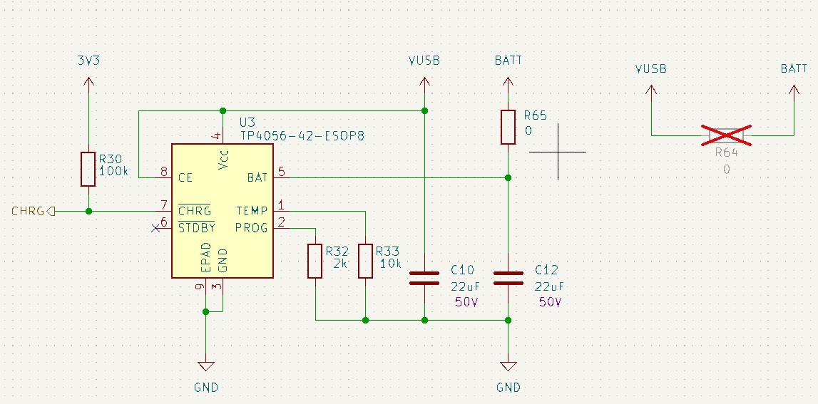
VUSB → VBAT — routes USB bus voltage directly to the BATT rail, bypassing the battery
Charger output → VBAT — this jumper must be opened when running without a battery to avoid a power conflict between the USB supply and the charger output
With VUSB→VBAT closed and the charger output jumper open, the device runs from USB power with no battery installed. Useful for bench work and long-term wired deployments.
(Schematic screenshot: Power sheet — VUSB and charger jumpers)
Fix 7 — No 3.3V Available on the mPCIe Slot
Rev.1: The mPCIe connector only exposed the 5V and BATT power rails. Any module that needed a ready 3.3V supply and had no onboard LDO could not be used.
Rev.2: A solder jumper was added to optionally connect the main 3.3V rail to the mPCIe slot. Available current is limited by the AP2112K's output capability, but for low-power modules it is entirely sufficient — and having the option is better than not having it. The jumper keeps it opt-in so it doesn't interfere with modules that generate their own 3.3V.
(Schematic screenshot: mPCIe sheet — 3.3V jumper)
Fix 8 — Wrong I2C Bus Routed to mPCIe
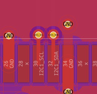
Rev.1: The original intent was correct in principle: dedicate I2C1 exclusively to the mPCIe slot so it is always free for expansion modules. However, due to a routing error I2C2 ended up on the connector instead of I2C1 — meaning I2C1 was being used elsewhere on the board and the slot got the wrong bus entirely.
Rev.2: Fixed. I2C1 is now correctly routed to the mPCIe connector as originally intended, keeping it exclusively available for plugged-in modules.
From the very beginning, the enclosure had one hard requirement: when DevPocket is magnetically mounted to a smartphone via MagSafe, it must not extend beyond the phone's footprint. This drove the outer dimensions to 64.6 × 74.6 × 20 mm — compact enough to sit behind most modern smartphones without sticking out.
(Photo : all devpocket mechanics)
The 20 mm thickness is not arbitrary — it is dictated directly by the internal stack-up. From bottom to top: the LiPo battery sits on the underside of the main PCB, then the board itself, then the mPCIe module plugged in on top. There is no wasted space; the enclosure height is exactly what the electronics require.
(Screenshot: cross-section view showing the internal stack)
Fabrication Method
The enclosure is FDM 3D printed, chosen from the start of the project. FDM is the obvious choice for an open-hardware project: the files are on GitHub in both STEP and STL format, anyone with a printer can reproduce or modify the enclosure without any tooling costs, and iterating on a new revision takes hours rather than weeks.
Bottom Shell — MagSafe Ring Pocket
The bottom shell has a dedicated recessed pocket for the magnetic ring. The ring is a standard neodymium magnet ring sold on AliExpress for MagSafe-compatible accessories — it comes with a self-adhesive backing, so installation is simply press-fit into the pocket. No tools required.
The pocket dimensions match the standard MagSafe ring geometry: 56 mm outer diameter, 46 mm inner diameter. This allows DevPocket to attach magnetically to any MagSafe-compatible phone case, a ring stand, or any ferromagnetic surface.
(Screenshot: bottom shell with the MagSafe ring pocket)
Top Shell
The top shell carries all the user-facing cutouts: the two tactile buttons, the USB-C connector, and the antenna port. It also includes channelled light guide channels — individual tunnels for each of the four WS2812B LEDs, with dividing walls between them to prevent light bleed between channels.
(Screenshot: top shell showing button cutouts and light guide channels)
Two variants of the top shell are published on GitHub:
Standard top — for bare DevPocket use
Sensor module top — with ventilation slots for air circulation around the ENS160/AHT20/BMP280 sensors, plus a slot for the display board that mates with the lid connector automatically when the case is closed
The top shell is the part you'll most likely customise when designing your own mPCIe modules — the rest of the enclosure stays the same.
Fasteners and Heat-Set Inserts
All threaded connections in the enclosure use M2 × 5 × 3.2 brass heat-set inserts pressed in with a soldering iron. Installation temperature should be approximately 10–20 °C above the filament's print temperature — for PLA around 225 °C, for PETG around 245 °C.
The knurled outer surface of each insert melts into the surrounding plastic and locks permanently as it cools, giving a clean metal thread that survives repeated assembly and disassembly without stripping.
Two screw types are used:
Application
Screw
PCB to bottom shell (standoffs)
M2 × 4 DIN 912 — socket cap head (hex key)
Top shell to bottom shell
M2 × 14 countersunk — DIN 965 / ISO 7046, 90° head, Pozidriv drive
Using countersunk screws for the shell halves keeps the outer surface completely flat — no protruding heads on any face of the device.
Light Guides
The light guides are custom-designed parts, printed on an SLA 3D printer in clear resin. SLA was the right choice here: the smooth, optically clear surface finish of SLA parts transmits light from the WS2812B LEDs far more efficiently than the rough, semi-opaque surface of an FDM print.
(Photo: light guides separately)
Each guide is shaped to route light from the LED position to the face of the enclosure, with the dividing walls in the top shell preventing cross-illumination between channels. That said — you do not have to print your own. The channel geometry in the top shell is compatible with standard off-the-shelf light pipe inserts if you want a simpler option. Files on GitHub
STEP and STL models for all enclosure variants are already published in the repository:
The enclosure is done and the device is fully functional as a portable air quality monitor. But during Rev.1 testing I found several bugs in the schematic that need to be addressed. In Log #5 I'll go through the Rev.1 mistakes in detail and show what changed in Rev.2 of the board.
In the previous log I introduced the air quality sensor module — now it's time to actually read data from it. The module carries three sensors over a shared I²C bus: BMP280 (temperature + pressure), AHT20 (temperature + humidity), and ENS160 (eCO₂, TVOC, AQI index). All three sit at fixed I²C addresses and are powered through the mPCIe connector from DevPocket's 3.3V rail.
Reading the Sensors — How the Script Works
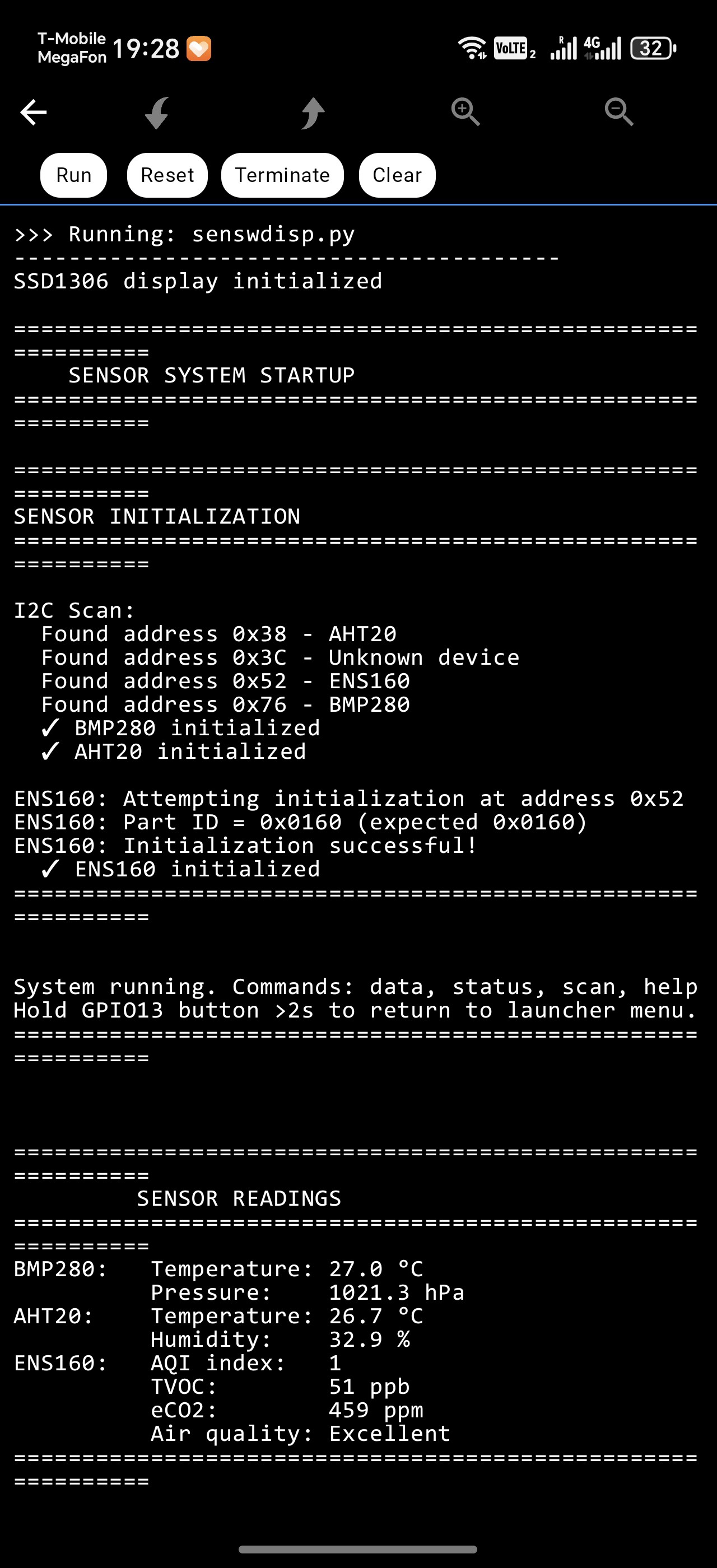
On startup, the script runs an I²C scan and initialises each sensor in sequence, printing the result to the console.The ENS160 is the most demanding sensor to initialise — it requires a hardware reset sequence (RESET → IDLE → CLEAR → STANDARD), and its Part ID (0x0160) is verified before proceeding. Once running in standard mode, it receives live temperature and humidity compensation data from the AHT20 on every reading cycle, which is mandatory for accurate eCO₂ and TVOC figures.Readings are updated once per second. The console microREPL output looks like this:
(Screenshot: console output with sensor init and live readings)
While the script is running you can interact with it via micro-REPL or any serial terminal:
Command
Action
data
Print a fresh sensor reading immediately
status
Show which sensors were found and ENS160 init state
scan
Re-run the I²C bus scan
help
List available commands
The four WS2812B LEDs on DevPocket each have a dedicated role in this script:
LED
Meaning
LED 0
Green — all sensors OK / Red — at least one missing
LED 1
Orange — USB charging in progress / Green — on battery
LED 2
Blue blink — I²C read cycle active
LED 3
Green — air quality normal / Yellow — warning / Red — poor
Going Fully Standalone — The Display Lid
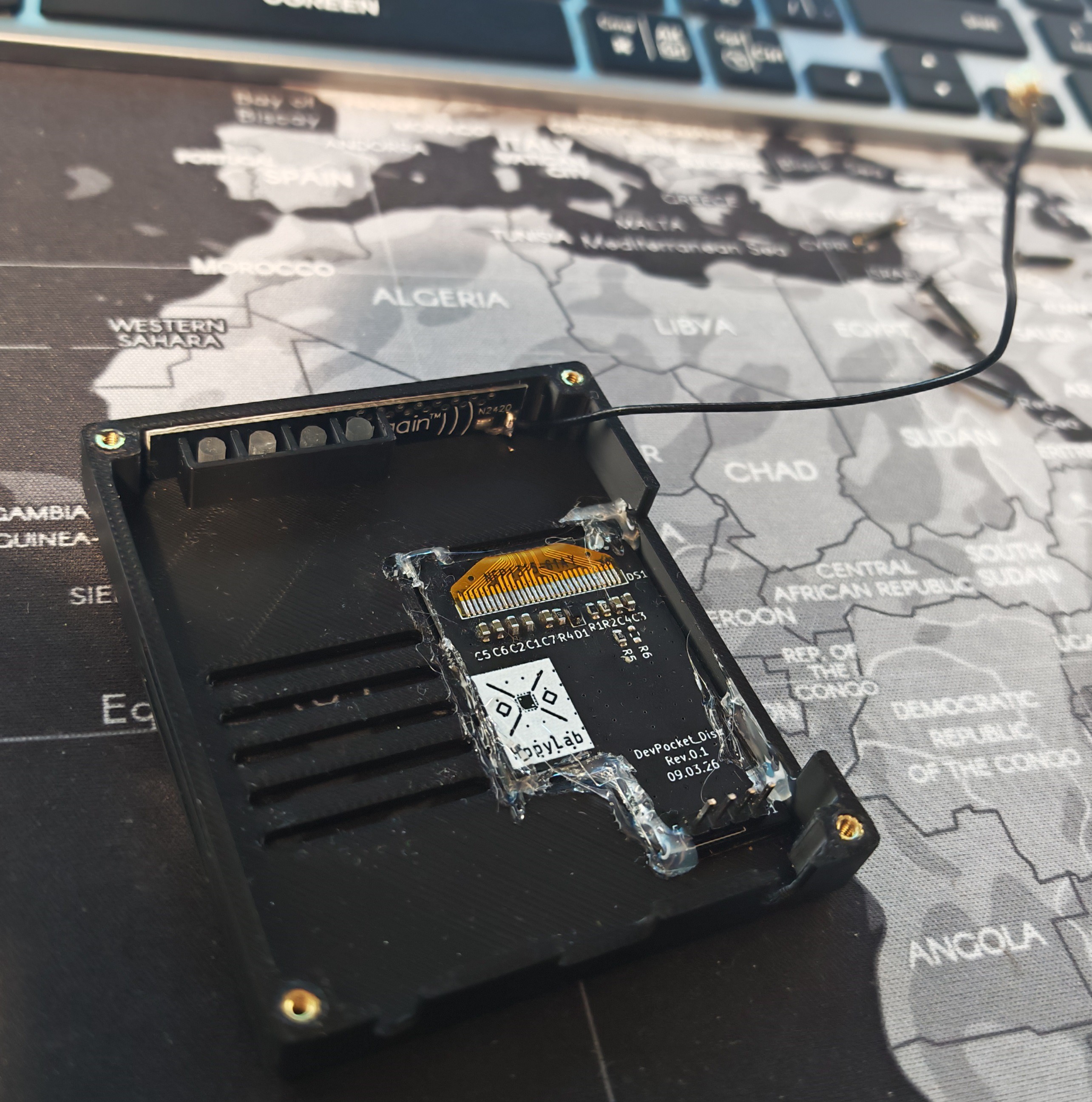
When I designed DevPocket I included two dedicated connectors on the main board: one for an OLED display and one for an LED matrix. The idea was to make a PCB that mounts inside the top lid of the enclosure — when you close the case, the connectors mate automatically and the display(LED matrix) is live without any extra wiring.
(Photo: top lid with the display board glued in)
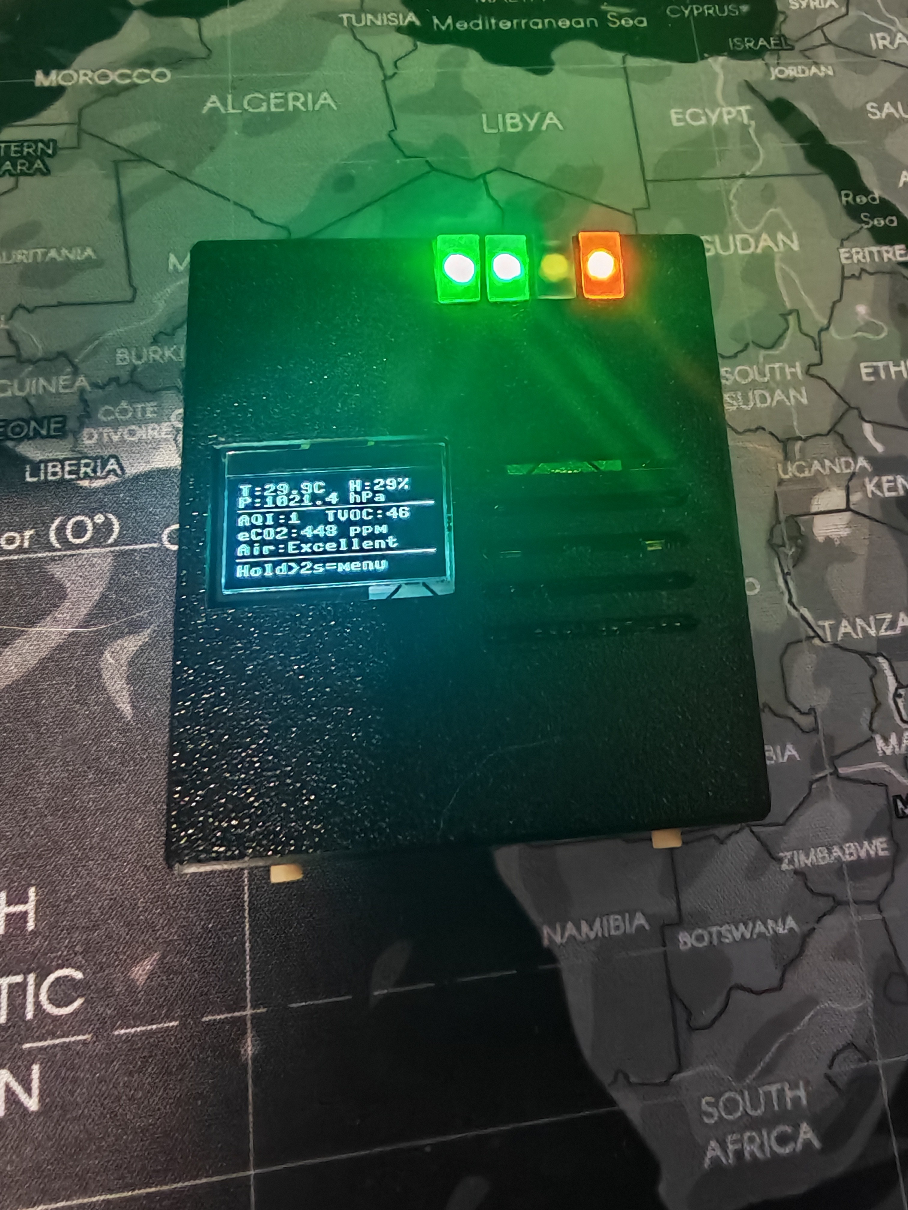
The display board uses a standard 128×64 SSD1306 OLED. It connects to the I²C bus as the sensor module, so the whole system — sensors, display, and main MCU — runs on two wires. The OLED layout for the air quality script fits all key data on the 64px height.Temperature and humidity sit on the top line, pressure on the second. Below the divider: AQI, TVOC, eCO₂, and a plain-English air quality description. The bottom status bar shows either a sensor warning (!Sensor miss), charging state, or the button hint (Hold>2s=menu).
(Photo: DevPocket with the sensor module and display running)
Returning to the Launcher
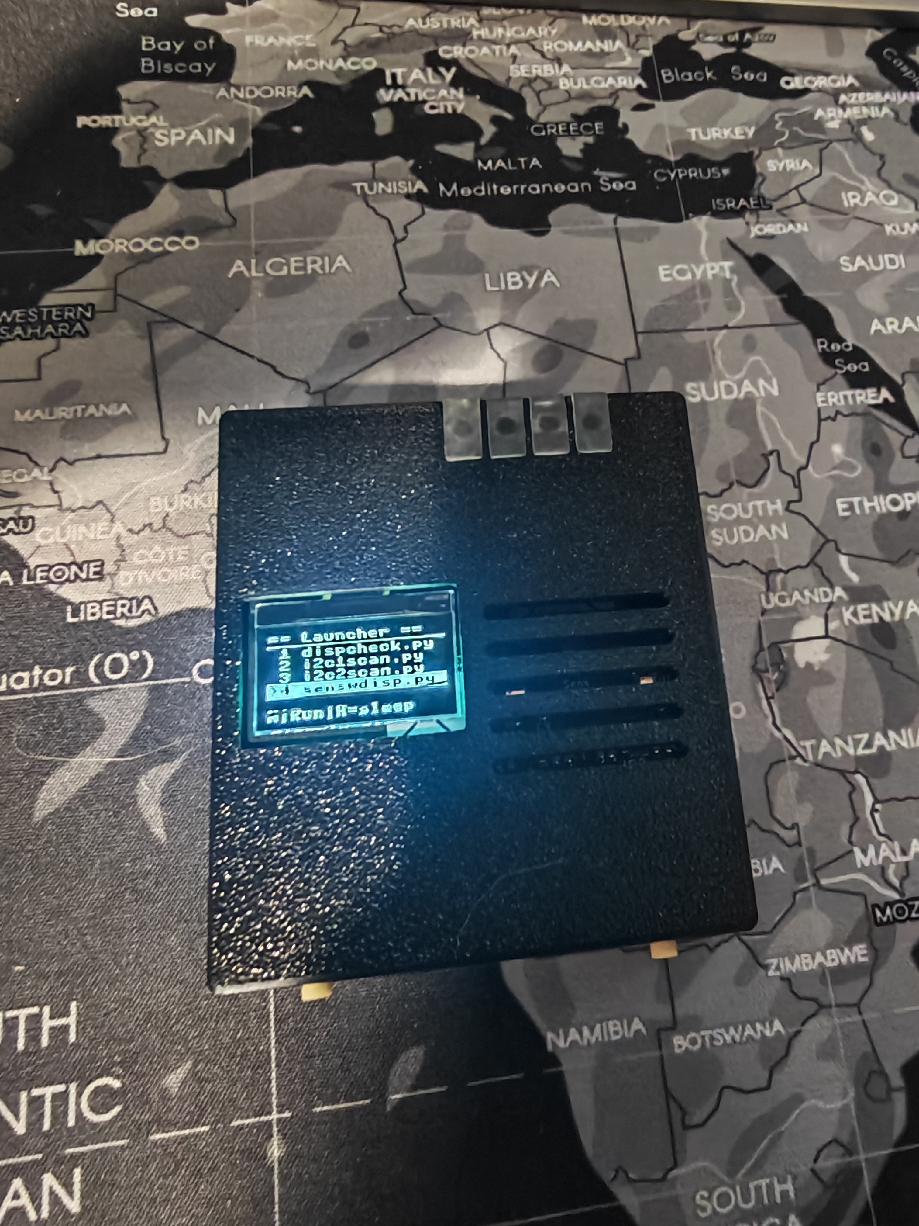
Since this script runs inside the launcher (described in Log #2), exiting back to the script menu is built in. Holding the NEXT button (GPIO13) for more than 2 seconds triggers a clean shutdown: the sensor power rail is cut via the PWR_SENSORS GPIO, the OLED shows "Returning to menu…", the LEDs are cleared, and a KeyboardInterrupt is raised — which the launcher catches and uses to return to the script selection menu. No reboot needed.
(Photo: DevPocket with display in the scriptselectionmenu )
What This Actually Gives You
At this point DevPocket is a fully self-contained device: battery powered, display on the lid, no phone or PC required. In practice I carry it as a portable air quality monitor — drop it in a bag, pull it out, and the OLED immediately shows temperature, humidity, pressure, CO₂ level, and an AQI rating for wherever you are. The same unit also doubles as a battery-powered I²C scanner — just launch the scanner script from the menu instead.
What's Next
In Log #4 I'll cover the mechanical side — how the enclosure is designed and assembled, and I'll publish the STEP models for the current enclosure revision to GitHub so you can print or modify your own.
The first boot went smoothly — no magic smoke, no unexpected behaviour. I went through the hardware checklist one by one:
Power system — the TP4056 charged the LiPo correctly via USB-C, the TPS61023 boost converter brought up the 5V rail cleanly, and the AMS1117-3.3 LDO delivered stable 3.3V to the ESP32
Microcontroller — the ESP32-WROOM-32UE enumerated correctly over the CP2102GM USB-UART bridge and responded to flashing without issues
WS2812B LEDs — all four addressable RGB LEDs responded to a test pattern
Tactile buttons — both GPIOs registered clean transitions with debounce
DevPocket then connected to an Android phone and was immediately recognised by micro-REPL. One small surprise: the phone started charging the device over USB without any prompt or permission request. This is standard USB host/peripheral negotiation behaviour — the phone detected DevPocket as a device and pushed VBUS. It's not a problem in practice, but worth noting for battery-conscious use cases.
(Photo: DevPocket during first power-on)
First Sketch — Script Launcher with Deep Sleep
For the first real firmware I wanted something immediately useful: a launcher that lets you navigate and run scripts stored on the ESP32's filesystem directly from the two hardware buttons.
Everything is controlled with two buttons:
NEXT — scrolls through the script list
RUN (short press) — launches the selected script
RUN (hold >2 sec) — sends the device into deep sleep
When a script runs, it executes inside the launcher's context. When it finishes, DevPocket returns to the menu automatically.
(Screenshot: micro-REPL session on Android)
First Module — Air Quality Sensor Board
The first mPCIe module I designed alongside the main board is an environmental monitoring module — something I've wanted to carry around for a long time to assess air quality wherever I happen to be.
(Photo: mPCIe sensor module)
The module fits the standard mPCIe half-size form factor and plugs directly into DevPocket's expansion slot. It carries three sensors on a shared I²C bus:
Sensor
Measures
I²C Address
BMP280
Barometric pressure, temperature
0x76 (SDO → GND)
AHT20
Relative humidity, temperature
0x38 (fixed)
ENS160
eCO₂, TVOC, AQI
0x52 (ADDR → GND)
Power architecture is a two-rail design. The ENS160 requires a separate 1.8V supply for its VDDIO digital interface, generated by an XC6219B182MR-G LDO. The sensor core VDD runs from 3.3V via a second XC6219B332MR-G LDO, providing local regulation and decoupling independent of the main board's rail. The BMP280 and AHT20 run directly from the module's 3.3V rail.
All three sensors communicate over I2C1 (SDA/SCL routed through the mPCIe connector from ESP32 GPIO32/33). The ENS160 INT line is routed to IN1 on the connector for interrupt-driven readout when needed.
I²C Scanner — First Utility Script
Before writing any sensor code, I ran an I²C scanner to verify that all three sensors were electrically present and at their expected addresses. This is a universally useful tool — any time you're debugging an I²C bus on an unknown device, you just run it on DevPocket.
(Screenshot: I²C scanner output on Android via micro-REPL)
The scanner swept addresses 0x08–0x77, and all three sensors responded at their expected addresses: 0x38, 0x52, and 0x76. No bus errors, no address conflicts — the module schematic checked out.
What's Next
The next natural step is to read actual data from all three sensors and display it on the OLED — so you can get a full air quality readout with no phone attached at all. That sketch is in progress now, and it'll be the subject of Log #3.
One more thing: during this testing phase I found several bugs in the Rev.1 schematic. A Rev.2 board is already being prepared. I'll detail exactly what went wrong and how I fixed it — probably in Log #4 or #5.
When I designed DevPocket around the ESP32-WROOM-32UE, I made a deliberate choice: pick the UE (external antenna) variant instead of the standard E variant with a built-in PCB trace antenna. The reason is simple — DevPocket is a universal tool. It goes into a magnet-ringed plastic enclosure, gets mounted to phones, placed near other electronics, and used in wildly different environments.
By routing the antenna connection to a standard U.FL/IPEX connector, I leave the door open: you can install a short stubby antenna for desktop use, a high-gain directional antenna for range testing, or a flat flex antenna if you're tight on space. The hardware doesn't dictate the RF strategy — you do.
What I Actually Chose For the reference build I needed an antenna that was:
Cheap (this is a hobbyist open-hardware tool)
Compact enough to fit inside or flush against the enclosure
Tuned for 2.4 GHz (Wi-Fi b/g/n + Bluetooth)
Available widely (AliExpress, LCSC, Mouser)
I settled on a small 2.4 GHz PCB antenna with an IPEX MHF1 connector — the kind that costs $1–2 and is commonly used in routers and IoT devices. The real question was: how well does it actually perform once it's inside a plastic enclosure surrounded by a PCB and a LiPo battery?
That's where the NanoVNA comes in.
A Quick Primer: What is SWR and Why Does It Matter? SWR (Standing Wave Ratio), is a measure of how well an antenna is matched to the transmission line (in our case, the 50Ω trace from the ESP32's RF output to the antenna).
When RF energy travels down a transmission line and hits an antenna with a different impedance, some of that energy reflects back toward the source instead of radiating into the air. These forward and reflected waves create a standing wave pattern. SWR quantifies this mismatch:
SWR = 1.0 — perfect match, 100% of power is radiated (theoretical ideal)
SWR = 1.5 — about 4% of power reflected — excellent for real-world use
SWR = 2.0 — about 11% reflected — acceptable
SWR = 3.0 — about 25% reflected — poor, noticeably degrades range
SWR > 3.0 — the antenna is significantly detuned
For Wi-Fi at 2.4 GHz, a target of SWR ≤ 2.0 across the band (2400–2500 MHz) is the practical goal. The NanoVNA measures this directly by injecting a swept RF signal and measuring the reflection coefficient (S11).
Why measure in three conditions? An antenna doesn't exist in a vacuum — it exists inside an electromagnetic environment. Its resonant frequency and impedance are affected by everything nearby:
The enclosure — even plastic changes the effective dielectric constant around the antenna element, shifting its resonant frequency
The PCB ground plane — a large copper pour beneath the antenna acts as a reflector and can detune it
The battery — a LiPo pouch is essentially a lossy dielectric slab that absorbs and scatters RF
This is why antenna datasheets are largely useless for embedded designs — they measure the antenna in free space on a reference board. Your actual SWR will be different. Testing in three progressive conditions lets you see exactly how much each layer of the design degrades (or shifts) the antenna's performance.
Measurements
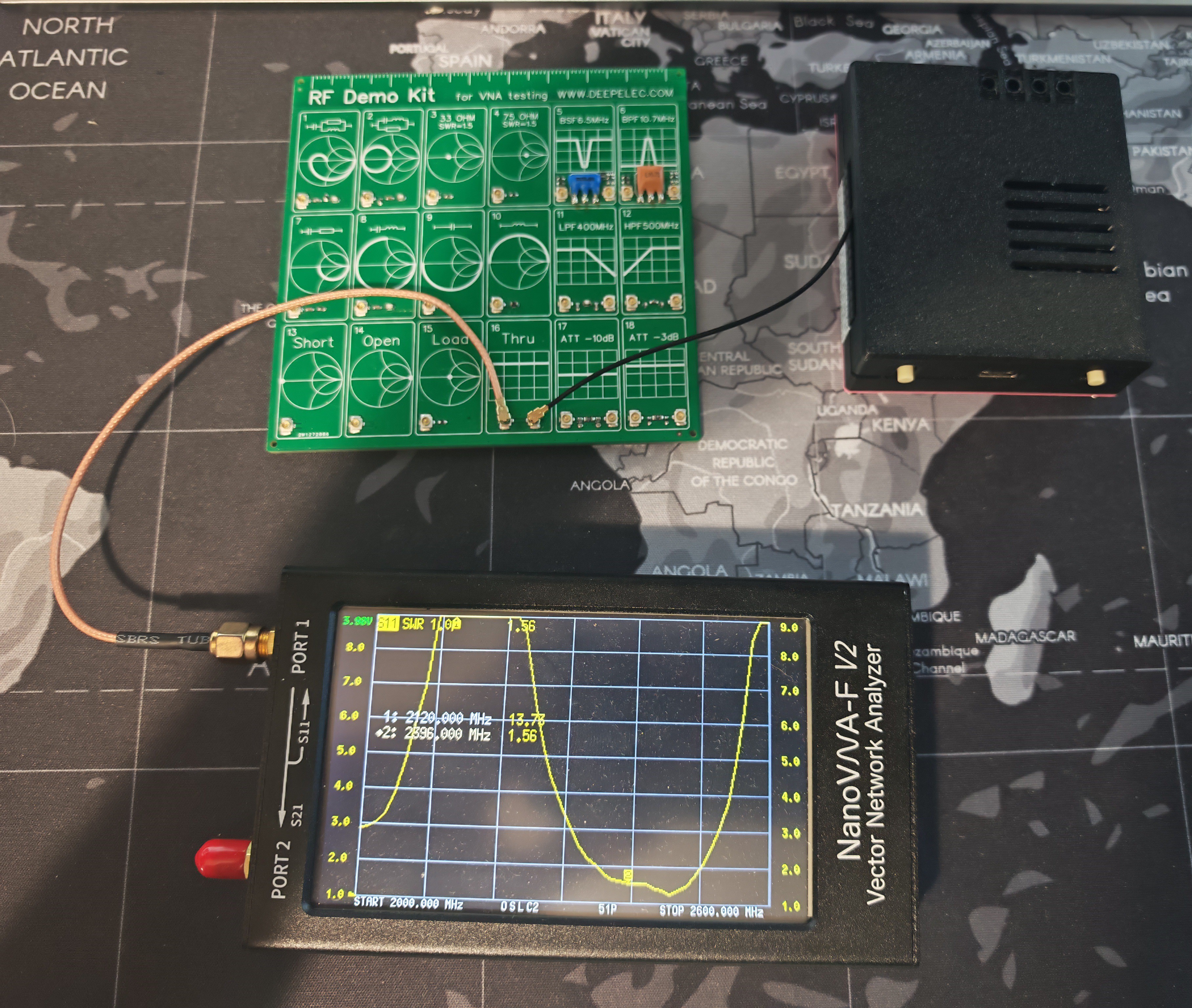
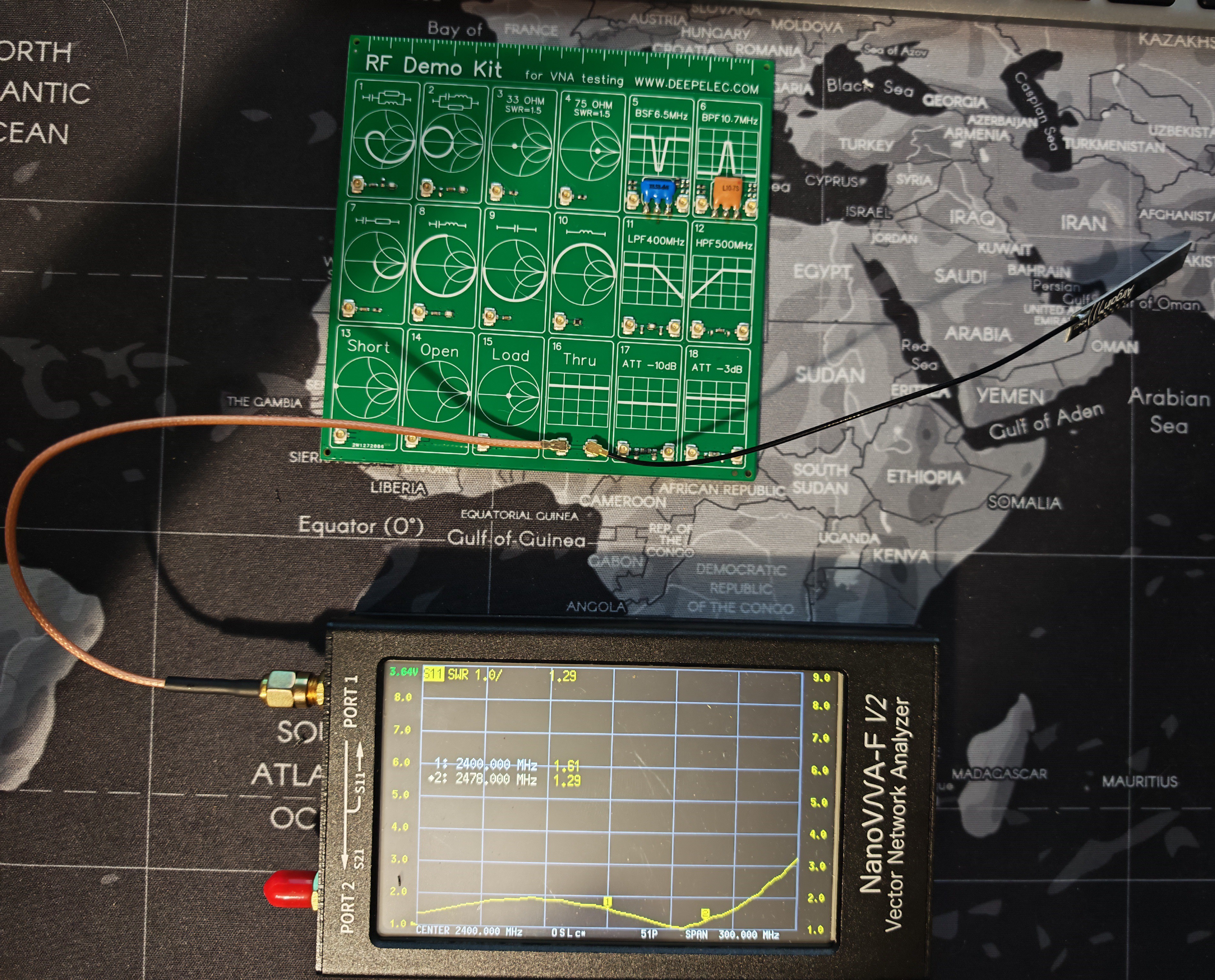
All measurements taken with a NanoVNA (calibrated with the SOLT standard at the U.FL reference plane). Frequency sweep: 2000–2600 MHz.
Antenna alone, no enclosure
SWR(2400MHz) - 1.61
Antenna in enclosure, no PCB
SWR(2400MHz) - 1.13
Antenna in enclosure with full PCB + battery
SWR(2400MHz) - 1.56
Takeaways The NanoVNA is an indispensable $50 tool for any embedded project with RF. Even if you're not designing the antenna yourself, verifying that the chosen antenna still works inside your specific enclosure with your specific board .
What's Next Antenna verified. Time to apply power for the first time.
In Log #2 I'll walk through the first boot of DevPocket: flashing firmware through the CP2102 bridge, what micro-REPL looked like on first connect from an Android phone, and the first scripts. I'll also cover the first real-world use case where DevPocket did exactly what it was designed for: untethered, on battery, magnetically clipped to a phone.
Stay tuned — and follow the project so you don't miss it.
By using our website and services, you expressly agree to the placement of our performance, functionality, and advertising cookies.
Learn More
 Ilya Egorov






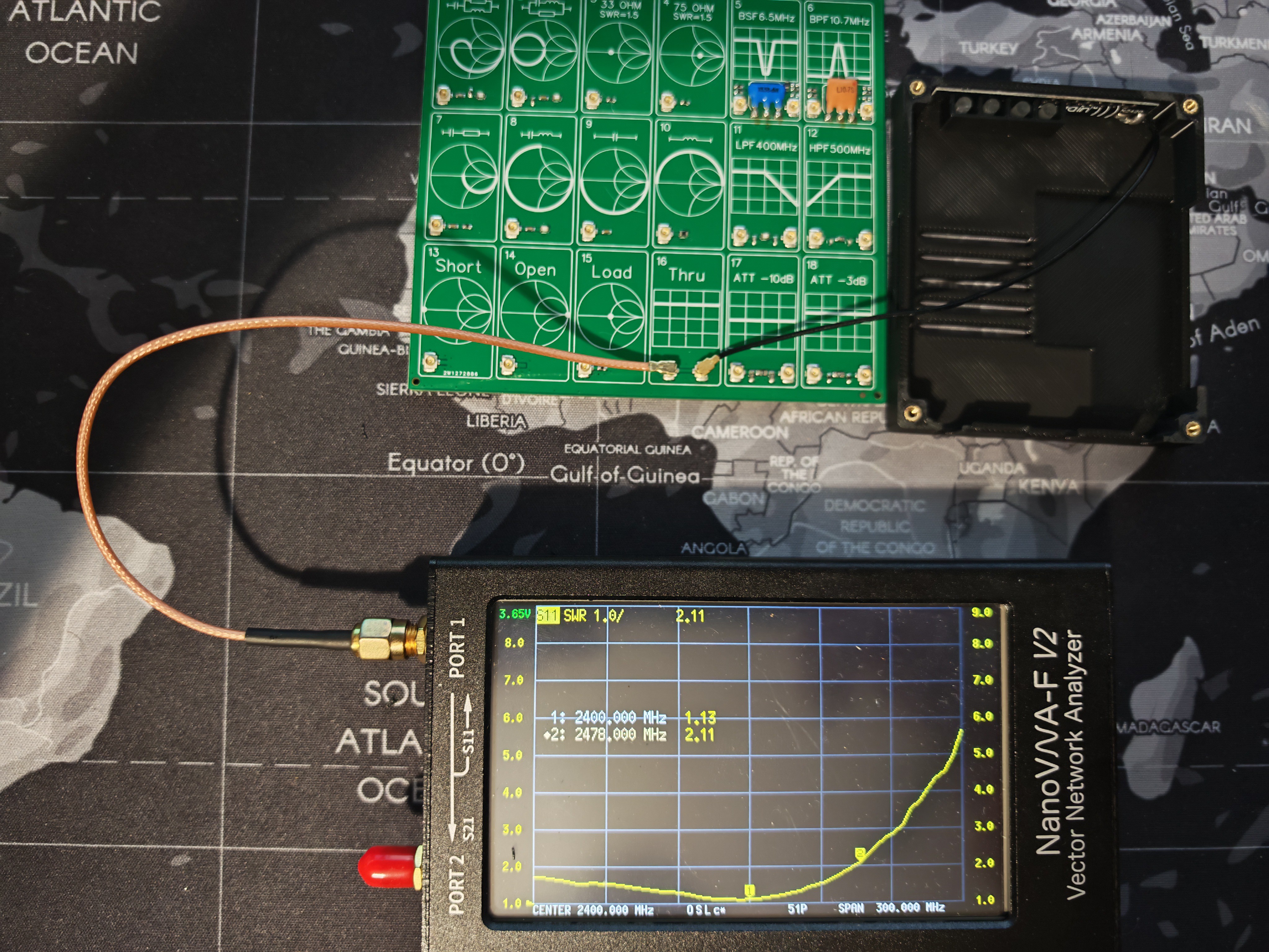 SWR(2400MHz) - 1.13