-
BM9 benchmarking results
09/14/2017 at 13:53 • 1 commenthttp://apollo181.wixsite.com/apollo181/experiment4-cpu-benchmark
I finally finished the BM9 benchmarking program in assembly code. The results: completes in 64 seconds with the clock running at 12MHz. Compared with the APOLLO181 finishing at 56 seconds running at 3MHz. I can assume that if I lowered my clock speed to the same, it will run four times slower, putting it at a run time of 256 seconds. I expect this because a one-instruction CPU is going to be less efficient especially with each instruction taking 4 clock cycles just for instruction fetching. This is because of my 16-bit memory bus instead of the 8-bit memory bus like on the APOLLO181. Also, I made my algorithm operate on 16-bit numbers instead of 12-bits. (Which makes the divider take 16 loops instead of 12). So I imagine if I reduced the complexity of my system down, it would operate roughly in the same amount of time.
As that website points out, the BM9 program was traditionally run in BASIC with an interpreter which drastically slows the operation, so a direct comparison is difficult. I also output the prime numbers in hexadecimal - I didn't bother to convert to decimal. Other notes from the APOLLO181 website:
- CDC CYBER 171, a late-1970s mainframe-class supercomputer, which run "BM9" (in Basic) in only 5 seconds (ranked 1st)
- TRS-80 Pocket Computer, which painfully run "BM9" in 55830 seconds (ranked last)
- 45 seconds for the DEC PDP 11/70 (ranked 5th)
- IBM 3033 (1977) run BM9 in 10 seconds (ranked 2nd)
- The Apple II Plus (1979) equipped with MOS 6502 microprocessor run BM9 in 325 seconds (ranked 15th)
- APOLLO181 would rank 6th
- As is, my one-instruction CPU would rank about 11th running at 3MHz (TTL speeds) - still faster than any of the 6502 systems
So now, I have to think where I want to go next. I may come back around and work on the TTL design.
Here is a link to the paper which has all of the results:
http://www.mwigan.com/mrw/Pubs__ICT_and_its_Impacts_files/82%20MICSIG%20ACS1-25.pdf
-
16-bit Dividing
09/12/2017 at 17:54 • 0 commentsI've been programming furiously. I have 16-bit functions going - Add, Subtract, and Divide. And I have 8-bit multiply going. I've changed from putting the operands on the stack to having a dedicated memory location for them. I have so much memory, it's easier/faster just to hard-code specific locations for them. Next I'm going to implement the BM9 benchmark program as seen in the APOLLO181 website:
http://apollo181.wixsite.com/apollo181/experiment4-cpu-benchmark
This is also where I got my divider program, except I adapted it for 16-bit words. I've added these functions to the ROM as subroutines which I can call and return to my main program. I still have plenty of room in the ROM and RAM, so I don't think I will run out any time soon. I'd like to get the BM9 program into the ROM so if I ever get to the TTL version of the CPU, I can compare its run time to the FPGA version.
-
Back up to speed
09/06/2017 at 15:54 • 0 commentsI've completed the hardware and software updates for the 16-bit register address bus. I now have the monitor program running (not really a bootloader which I've been calling it). I have also updated my PUSH/POP commands along with my CALL and RETURN commands. So my stack is working correctly again. I also implemented putting variables onto the stack and using them in functions. The first function I put into the ROM is the BinaryToASCII function. I push a byte onto the stack, and then call it. It converts the byte into two ASCII bytes which it then sends over the UART. I made this function so I can use it in my monitor program to read memory locations and display them.
I've found coding goes much faster now with the new architecture. There's a lot less mental gymnastics. This makes it a lot more fun to code for it as well.
-
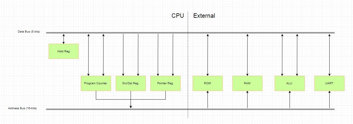
Top-level block diagram
09/05/2017 at 14:42 • 0 commentsI redesigned the top-level block diagram so that it illustrates the new datapath better. It's much simpler than the previous one, but it doesn't have the TTL chips called out. This makes it simpler to understand the operation of the different functions. I'd like to be able to animate it and make a gif out of it so I can show what happens in the 6 clock cycles per instruction, but draw.io doesn't support it. I would like to have a better flowgraph program, but I do like open web-based tools.
![]()
Breaking down the system like this makes it much easier to understand its simplicity. The CPU only really controls which of the three 16-bit registers control the address bus, and then decodes the address bus for reading/writing of its own 16-bit registers to/from the data bus. It starts to look a lot like a normal 1970s CPU interface (like a 6502 for example). Perhaps I could make two different PCBs - one for the CPU and one for the external peripherals - just to show what parts the CPU could be if put into an ASIC.
-
16-bit register space implemented
08/31/2017 at 19:29 • 0 commentsI have updated the VHDL code to implement the change to a single 16-bit address space which includes the register space and the RAM/ROM space. It seems to be working ok.
I'm rewriting the bootloader for this new architecture. I'm still debugging, but it is definitely easier and more fluid to write code for this. However, the code is generating almost twice the memory size as expected (about 1.8x) even though it's fewer instructions. I'm pretty happy with this change. I notice I do a lot of LOAD-type commands which are now more straight-forward since I'm just copying from the ROM.
I've found in this iteration the ALU and pointer registers are really more like peripherals. It's almost like if you took a 6502 and added a co-processor for floating bit operations, except all operations are done in the peripherals. So outside of the peripherals and memory, it's just a simple state machine, a couple of counters to hold the program counter, and a couple registers for the source/destination address. If I was in the early 1970s, I could have made an ASIC with this and then bring out the data and address bus to an external RAM/ROM and peripherals like an ALU or UART, etc. I may reorganize my block diagram to show this better. In doing this project it makes me realize that an ALU is not necessary for a minimum-viable CPU (Turing complete).
-
16-bit register/memory space
08/29/2017 at 14:41 • 0 commentsOne thing that's been very annoying in coding is how I interface to the memory. I have a 16-bit page register that allows me to access 128 memory locations with the source/destination bus. So when I push/pop I have to change my memory page to the stack. Then I lose access to my other variables. Copying a variable onto the stack is tough because I have to store it in the few registers I have, change the memory page, and then copy it back without disturbing those registers.
I would really like to be able to access the whole 16-bit memory at any time. The old 6502 allows you to access the whole 16-bit memory space and I'm jealous. This would let me pop/push without losing access to my other memory space. I can move variables onto the stack easily. And I can transfer from anywhere to anywhere in my memory very easily.
Implications:
So the memory map will look something like:
0x0000 0x00FF Function Registers 0x0100 0x7FFF ROM 0x8000 0xFFFF RAM - Each instruction now goes from 16-bits to 32-bits. So my programs increase in size pretty quickly.
- I'll have to rewrite all the code I previously wrote.
- The new instruction cycle would be two fetches for the source address, copy the source data to a temporary register, two more fetches for the destination, then write the temporary register to the destination - 6 clock operation. Boy this went up fast from my original desire for 1 clock per instruction!
- I won't need a LOAD register anymore. It will be trivial to put a 256 constants in the ROM and do a transfer from there. This removes all the LOAD register chips.
- The pointer address register will have to change to point to a 16-bit address, so a HI and LO register.
- I'll have to change the boot vector to 0x0100.
- I'll have to decode a 16-bit address now, but maybe I can just check if the upper byte is all zeros.
This is almost a complete tear-up of the design. However, it will be much easier and elegant to code for this CPU (and more fun). And I don't think it will increase the chip count
-
Benchmarks
08/01/2017 at 16:56 • 0 commentsI completed a simple 8-bit x 8-bit multiply function (iterative adds). I decided to do a quick benchmark to check its performance. Since this is an iterative add function, the worst case is FF x FF. It takes 1.61ms to perform with the clock running at 12MHz. So it takes 19,397 clock cycles to perform the operation. That's a lot of moving. If there's 256 loops, then it takes about 76 clocks per loop. There's currently 3 clocks per instruction, so about 25 instructions per loop. That sounds about right.
A better algorithm would speed this up like the shift-and-add algorithm (probably). But it's good to get a baseline. The number of loops is really the killer. A shift-and-add algorithm does I think 8 loops with an add and a shift right each loop. Of course, in the best case, my algorithm takes zero loops, so it's possible to be faster, but statistically I'm sure it's slower.
But now I can store this function in the ROM and call it whenever I need to do a multiply. However, I have it pointing at dedicated memory locations. I need to work on using the stack to pass values to functions instead.
-
Stack code
07/31/2017 at 17:57 • 0 commentsI've finished the stack code including pop,push,call,return. So that brings me to all of the following instructions implemented:
- move
- load (immediate)
- memload (immediate)
- memread
- memwrite
- jump
- branchif1
- pop
- push
- call
- return
- rotateleft
That should give me quite a lot to make some real programs now (on top of the inherent functions of the ALU). I'll need to bring up some better debug tools next. Memory inspection. Probably enhance my bootloader. Maybe start on an emulator.
-
Focus
07/20/2017 at 15:54 • 0 commentsI realize in looking over everything I'm doing for this project, it's actually several projects that are falling under one umbrella.
- A TTL design (which is only at the design phase)
- An FPGA design (which is fully working)
- An assembler (which is fully working)
- Software code development to implement macro-functions which emulate normal architecture instructions (significant development)
- Software code development to implement more advanced features like a stack and ASCII conversion
- Emulated hardware on a PC for easier debug (not started)
- Emulated hardware on a PC as a video game (not started)
Each of these can be a separate project. Looking over other projects, some people's whole project is to develop an FPGA microprocessor which is only one component for me. Considering I have very little time/energy to devote to this project, I need to decide which components to focus on.
However, there is an underlying commonality which is the architecture. All of these assume a similar architecture even if they have different implementations. The FPGA doesn't use tri-state buses, but the TTL circuit does. It doesn't even matter if the TTL version has a single source/destination bus, and the FPGA has two separate ones, or even if it's emulated hardware. As long as they can all execute the same code, then I would say they are the same. I have to admit, I'm pretty happy with the FPGA version because I can change it very quickly and have decent debug capabilities with the simulator.
I guess what I'm saying is I may delay building the TTL version for now, but keep the design so it can easily be built. I'd like to focus on developing the software and run it on the FPGA. The software development has been a lot of fun, which is why I keep thinking about making a video game about it similar to Human Resource Machine or the Zachtronics games. If only I had more time/energy, but my priorities are family->work->hobbies, I'm left with maybe an hour a day for the last one and no energy.
-
Infamous load function
07/10/2017 at 13:59 • 0 commentsI've been changing my datapath to only have a single source/destination bus. I've run across one problem with the LOAD register. Normally, I will grab the data from the source and store it in the temporary holding register, then write the temp register to the destination on the next cycle.
When I do a LOAD, I take the source address and put it into the LOAD register. Which means I need to know both the source and destination at the same time. Or, the temp register doesn't have the valid data I need to put into the LOAD register.
- The best idea I have come up with so far is to have ANOTHER temporary register which holds the source destination only for the purpose of putting it into the LOAD register. It's not a great solution.
- I also thought about doing a look-ahead to see if the next instruction points to the LOAD register.
- Or maybe a look behind to pull the previous byte from RAM into the LOAD register. After all, the data is in the RAM - I just need to get it out again. But that means more extra logic which means more chips.
- Alternatively, I can ditch the LOAD functionality altogether. Instead just store 256 bytes in the ROM - one for each constant. So a LOAD would then be changing the data ram pointer to the constant area, then copying the correct constant out. And then change the data ram pointer back to where it was previously. It's a less elegant design, but it would be fewer chips. It might be problematic because what if I want to load a constant into the data ram pointer?
- Maybe I could change how the LOAD register works. In other words, the LOAD register always contains the previous source location. So the LOAD register would only be valid for one instruction. That may be an acceptable solution. I'll have to check to make sure that logic works without adding more hardware.
One-instruction TTL Computer
A breadboard-able computer which uses only a single instruction - MOVE