-
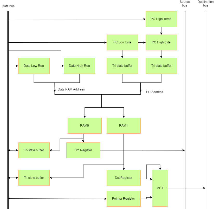
The One RAM
05/03/2017 at 19:58 • 0 commentsI've modified my design to use one RAM instead of two. The control state machine has been expanded to three repeating states: fetch source, fetch destination, execute. Seems to be clicking along no problems in simulation. It saves me 3 chips by doing this. I'm not sure why I would ever need to, but I could pass the source and destination registers to the databus through the tri-state buffer used to write/read the RAM. It might be worthwhile mapping these to addresses. I don't think it would cost me any chips, so I get it for free. Who knows what tricks those clever software engineers can come up with.
![]()
-
Old but fitting
05/02/2017 at 23:48 • 1 comment![]()
-
Artix-7
05/02/2017 at 21:54 • 1 commentI recently got an Artix-7 development board: the Digilent Cmod for my memristor project. But I realized I could try to implement my architecture in this board to give it a whirl in hardware. It has a UART interface and an on-board SRAM just like the one I plan on using. Well, it has ONE ram chip and my design needs two.
![]()
I got thinking that maybe I don't need two RAM chips. It would be an easy way to cut down on my chip count. But it would take 3 clock cycles to execute an instruction instead of two. That's not a terrible tragedy. It's also a lot less wiring. Each chip will have an 8-bit bus hooked up to it. And then I would only need one ROM chip as well. And if I got creative with the controller, I could still execute in two clock cycles for operations which don't need to access the memory. Then I could implement the whole thing very easily on my Artix board. I could check to make sure the timing is all correct, and I could implement the UART chip on there as well. I think I can do the ROM inside there as well for a simple bootloader. I could even pass the buses out the pins of the module and into my logic analyzer for debugging. Then I'll make it old-school and use the real chips.
-
UART
05/02/2017 at 16:44 • 2 commentsI've been looking into UART chips. Even if it's not explicitly stated in my goals, I'd like to recreate the computer design experience of the 1970/1980 era. The first UART chip came out in 1981 (The 8250), so I think it's within the spirit of the project to use its successor the 16550 (specifically the Texas Instruments PC16550D). It has an 8-bit parallel interface and a built-in FIFO. Makes it pretty easy to connect to my data bus. And I can connect the serial side to a UART-USB bridge cable. This will also need a crystal, but I could consider using the same crystal for my system clock (depending on how fast I can run my processor). But I don't think it needs any other chips, so it's a pretty nice addition to my design. I may need one more tri-state chip to interface the control/status lines. I'll have to consider if there's an easier way to do bit-wise interfaces to cut down my chip count.
-
Data memory interface done
05/01/2017 at 19:34 • 0 commentsI believe I have the data memory interface done. At least it's simulating correctly. That was a bit of a bear. Next up is the program counter reading onto the databus. Should just be two tristate buffers. Then bootloader! I'll need two 8-bits ROMS to go alongside the two RAMs. I looked at Flash-based memory, but the problem is they are mostly 3.3V. The rest of my chips need 5V and I'd prefer not to put in extra level-shifting circuitry. But I can put these right next to my RAM chips.
I figure I'll use the most significant bit of my address (A15) to select between the RAM and ROM. I'll put the ROM at A15=0, so when I reset my program counter, it will point to the first instruction in the ROM. Then I can run some piece of ROM code which grabs data from the serial port and loads it into the RAM, and then jumps to the RAM code. Or just some other interface which lets me choose what function I want. Maybe I'll have an SD card interface and transfer the code from there into RAM and then execute it.
$0000 - $7FFF ROM $8000 - $FFFF RAM Chip count: 20! plus decoding chips (at least 2 more probably 4) plus 2 Instruction ROMs plus 2 for PC reading
-
Asynchronous woes
05/01/2017 at 17:33 • 2 commentsMy RAM is asynchronous which means it can be written/read independent from the clock. This gives me trouble in my VHDL simulation. I found out that Vivado doesn't indicate when a signal glitches. I know Modelsim does. I was seeing my RAM contents getting changed at strange addresses when the write line was not changing. I knew this could be a problem since the control lines going into my RAM come out of combinational logic. Normally this is a big no-no, but I'm trying to cut corners. I may do something like gating the write signal with the clock, so it only changes on a certain clock level. This does fix the glitching in simulation. Gating with the clock is also a big no-no, but I'm still looking at bending the rules to keep things simple and not add too much extra logic.
However, I was also expecting Vivado to tell me when a signal glitches. Of course, it's possible there's an option to set, but I don't see a whole lot of options. I am thinking of trying out GHDL, but that's another investment of time to set it up and learn. If I get too many more problems with Vivado, I will start looking at jumping ship.
-
RAM->RAM
04/30/2017 at 19:21 • 0 commentsI realized I have yet another problem - I can't do a RAM->RAM transfer. At least not in a single clock cycle. I can only address one location in memory at a time. I suppose I can do a RAM read in one instruction, and then a RAM write in a second instruction. But I'm not sure what to do if the software tries to perform a RAM->RAM transfer. I could try to set it up so that the destination address takes priority. So it will write back the same data that's in there. At least I think that's what it would do. Maybe at some point I could have exceptions, but my chip count is already getting uncomfortably high. I do have to build this thing at some point.
-
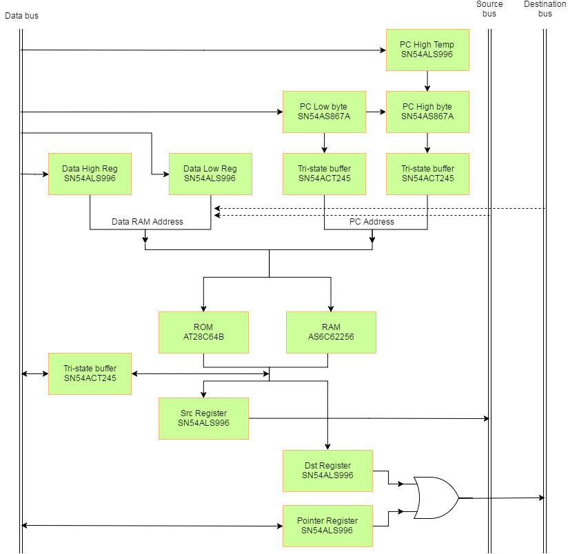
Updated RAM interface
04/30/2017 at 18:51 • 0 commentsMy RAM interface is a little complicated, so I updated my block diagram. I didn't get it quite right the first time. I'll have to update it again once I add the data bus access to the program counter. I figure it's costing me about 8 extra chips to do a common data/instruction memory. It's quite a cost when the rest of the system is about 15 chips. I think it's going to be worth it though. The ability to load programs by running a program will be worthwhile once I get a bootloader and UART interface working.
![]()
-
Program counting
04/29/2017 at 19:14 • 2 commentsI got the program counter chip simulated in VHDL and test benched. I added two of them into the top-level datapath. And added the high-byte temporary register. Simulated it again and it works just fine.
The only problem I didn't realize is I can't read the program counter as is. I can write to it, but the output is connected to the RAM chips. I would have to add some tri-state buffers to get the address out to the data bus which means 2 more chips. I'm aiming at minimal chip count, so I'll put this as an extra feature. I'm not sure how important it is to do read the program counter. Perhaps if you wanted to do a local jump you could read the value, add an offset, and write it back.
This project is coming along well. I have most of the important stuff in. I could start my build now if I wanted to. All of the important parts are there to run a program. But I think I'd like to make it a little more useful. I need to put the data RAM access in, and then I need to work on the I/O. And maybe a bootloader ROM.
FYI: 14 chips so far without address decoding which I expect to add maybe 2-3 more. Pretty good for how much it can do.
-
Program counter
04/28/2017 at 20:04 • 1 commentI believe I found my program counter chip. It's the Texas Inst. SN54AS867 - 8-bit loadable counter. Has a carry-out so I can chain two of them together. And it has a reset so I can bring it back to a known address easily. I'll have to decide how to do my startup though. I may want to execute instructions out of a ROM for a bootloader, and I'd have to have that at my reset vector. The Apple 2 had a ROM with a bootloader, but also a bunch of handy routines to help out programmers. Not as big of a deal now that memory isn't as much of a limitation, but something to consider. Perhaps if I get it up and running and find myself using the same routines over and over, maybe I could put them in there.
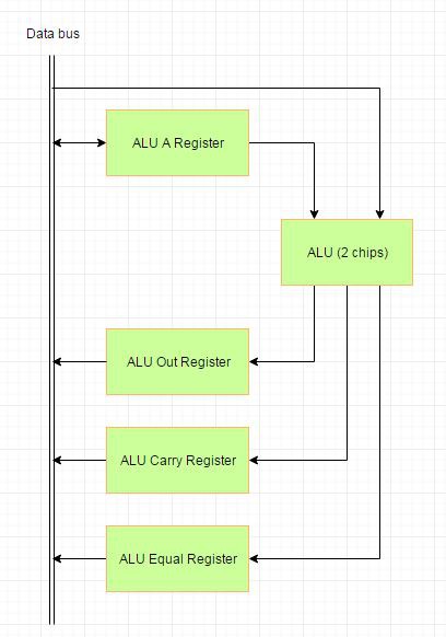
I've been working on some simple datapath block diagrams:
![]()
Of course, it still needs work on the data bus ram interface. At least two more registers to hold the data addresses. But it's a good start. Here's the ALU interface:
![]() None of the decoding/control logic is there, but I can add that later.
None of the decoding/control logic is there, but I can add that later.
One-instruction TTL Computer
A breadboard-able computer which uses only a single instruction - MOVE

 None of the decoding/control logic is there, but I can add that later.