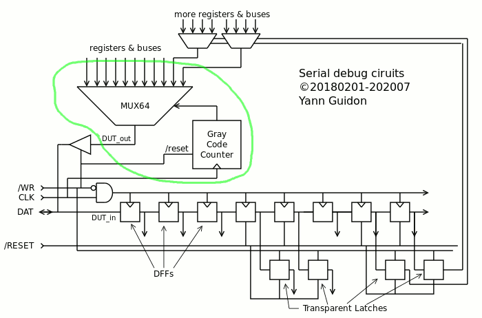
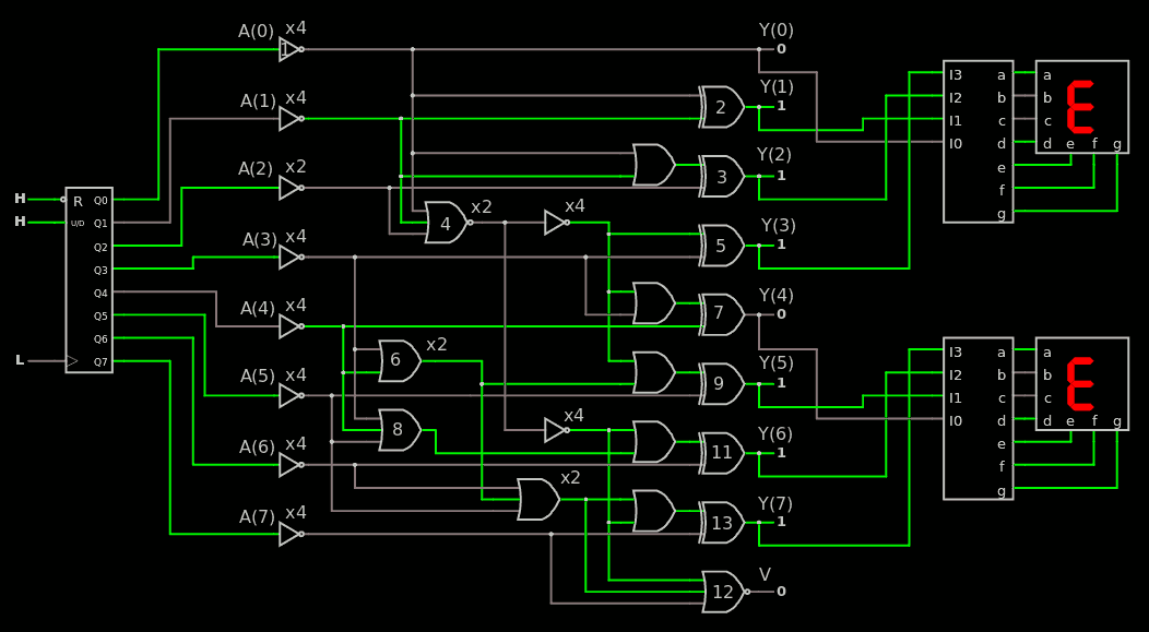
Today, after I designed the large MUX, I validated the part of the TAP that extracts information out of the core.
The Gray+BBT-BC combination has very good characteristics (fully asynchronous, glitch-free, easy to route, no select/clock/reset fanout problem) but at the price of some serious scrambling so I wrote the tools to extract the scrambling/permutation vector. Now the program test_readback.vhdl shows that I can reconstruct the original value from the serial output bitstream.
The vector is stored in the file PISO_permutation.out as a series of comma-separated decimal numbers and can be #included in other source code files. This file must of course be updated if the structure of the tree and the type of MUX are altered.
In practice, there are two uses :
shift bits in, 64 at a time, to get a snapshot of the selected signals. The 8 bytes must be descrambled together to make any sense.
Select one signal and spy on it with a 'scope for example. It could help with asynchronous signals, IRQ, event counters...
The extra optional MUXes are managed by other parts of the circuit, which are target-specific
The other half of the TAP is similarly split into a common/generic/core part and a target-specific one that can be adapted later. It is not shown on the above diagram yet but we can already see 2 cases :
some values of the shift register are transient and it's OK. Usually, these values are then MUXed with other internal signals and sampled when the core is stopped for example. So there is only the need of one DFF in the chain (you handle the MUX where you want).
some values must be persistent : their alteration during shift would just "confuse" everything so an additional memory cell is required. For example they hold a control code, or drive MUXes. The extra cell is is not necessarily an edge-triggered DFF because the value is already stable and the latch is controlled by /WR, not CLK : there is plenty of setup&hold margin there. A transparent latch is smaller and sufficient.
So two types of scan cells are required (persistent and transient), one with an extra latch. They are instanciated by the higher-levels of the system.
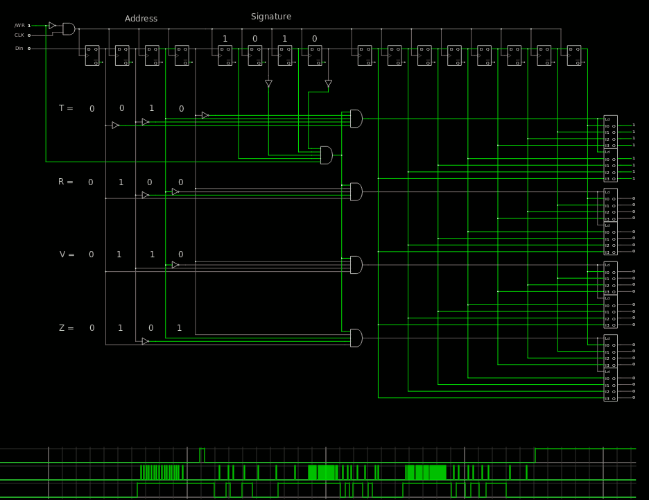
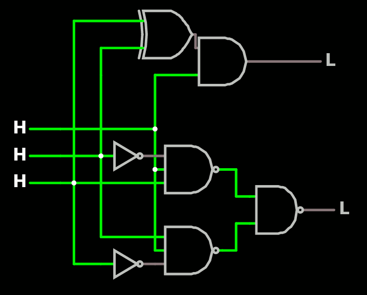
At the lower level however we can already provide safety features that also ease the rest of the design. The first thing to ensure is that the received bitstream is valid. A CRC would require too much effort (particularly on the control/host side) but a small signature is almost as effective (it doesn't provide signal integrity but the format is easily checked). And there could be several signatures, right ?
The "signature" so far is a byte that is shifted in at the end of the bitstream, as a suffix : the 8 bits are always held by the core TAP circuit and the value is examined last, before /WR goes up. A simple boolean circuit can then check if the latches may be updated.
And if there are several signatures, different sub-groups of latches can be selected ! New groups of latches are then formed from unused signatures to provide upwards compatibility. Invalid signatures are ignored and don't update the internal state or latches, yet affect the shift register.
The signature/select byte can take an easily-recognised value, which we can look up in the ASCII table.
The letter T comes first to mind, for Test : 01010100 is a nice-looking binary word, right ?
Do you want to read the Events ? type E, or 01000101 to write to the related latches.
Are registers interesting ? Try R : 01010010
Bus : B = 01000010
Core : C = 010000101
Inputs : I = 01001001
Load instructions : L = 01001100 (to feed into the instruction SRAM before the CPU boots)
Outputs : O = 01001111
etc. (you get the idea, and there is a significant addressing space)
The beauty is that this is a suffix value, sent just at the end of the data stream, before /WR goes high again. This control word will then select auxiliary MUXes for example. The control word as well as the end of the shift register can be read back from the PISO to provide a loopback feature and a simple sanity check for the debug system.
And as usual this releases pressure from the clock and RESET tree, as only a few essential signals require the /RESET line and the clock is inherently split into separate low-speed groups that are easier to place & route.
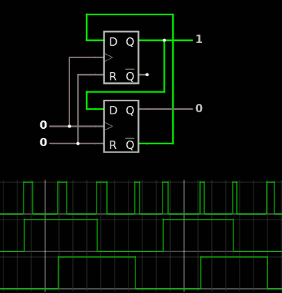
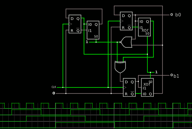
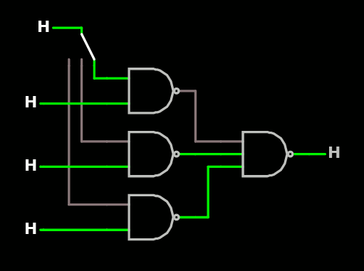
Simulation on Falstad validates the ideas :
In the above example, I have set all the "T" output by sending 0xFF followed by the 'T' character (MSB first). Setting /WR to 1 activates the latch/buffer while the others are left in their previous state.
This works despite the fact that the quad "latch" component of Falstad is edge-triggered : the group Enable signal is valid only when /WR is high, but it must go low before new data may be shifted in (and this is when the data is really latched and kept). At 10MHz there is enough setup&hold margin to prevent timing issues.
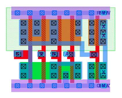
If you are unsure why all these efforts, compare the size of a MUX2 ASIC cell (which can be looped back to itself to make a T-lach) :
MX2 cell from wsclib013
With the size of a classic DFF cell :
DFNT1 cell from wsclib013
Some of these also require a RESET signal so the system is powered up in a coherent configuration, but that's a detail for another day (the YGREC8 only needs its internal FSM to be cleared and the rest follows, no need to spread a RESET signal all over the register set for example).
Overall, compared to JTAG, this type of TAP maps easily with short requests from debuggers for example. More complex features are then built as combinations, "sentences" of short messages. There is no internal FSM, no need to scan the whole chain just to get one value... OTOH it is not designed to be easily chained.
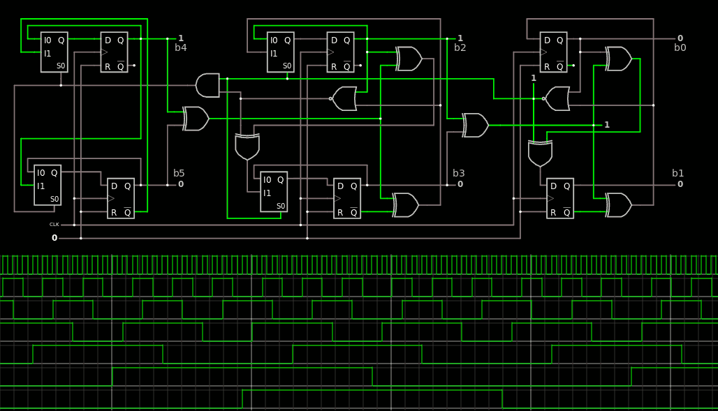
The Gray counter is now operational, now is the time for some MUXing !
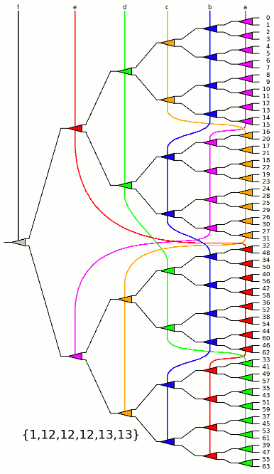
I already started to cover this subject in 25. MUX trees. The TAP/ directory now contains an interesting selection of MUX64 with various properties. I'll let you read the script and the output logs to see where it is going :
MUX64_behavioral.vhdl is just a plain dumb VHDL version that accesses the input vector as an array.
MUX64_BBTclassic.vhdl is an expansion of this, still using VHDL vector idioms.
MUX64_BBTgates.vhdl implements the above with individual gates, so we can start to see the properties : { 1, 2, 4, 8, 16, 32 } : not good ! This is indeed the pathological case.
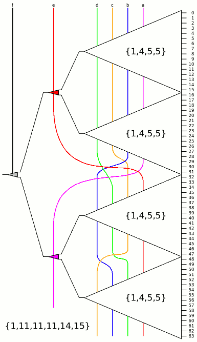
MUX64_BBTBC.vhdl uses 4 unbalanced sub-trees (MUX16_A.vhdl) and reaches the perfect score : { 1, 12, 12, 12, 13, 13 }however it might not be convenient to route. The sub-trees could get some treatment for local adaptation.
MUX64_BBTBC.vhdl with MUX16_B.vhdl is easier to route but worse { 1, 11, 11, 11, 11, 18 }
MUX64_BBTBC.vhdl with MUX16_C.vhdl is the worst : { 1, 10, 10, 12, 12, 18 }
MUX64_BBTm.vhdl is a modified version that reaches the closest suboptimal score { 1, 11, 11, 11, 14, 15 } with either MUX16_B.vhdl or MUX16_C.vhdl.
This is the best compromise I have found yet.
The README.txt explains how I came up with this permutation.
20200802 : Update !
As if this was not enough shuffling wires around, the PISO part has to send data "Most Significant Bit First" so all the scanning order has to be reversed.
Or simply the order of the inputs of each MUX is reversed.
That's what I did with the latest version of the tree : MUX16_Brev.vhdl MUX16_Crev.vhdl and MUX64_BBTrev.vhdl implement a MUX64 with reversed inputs.
20200808 :
See the log 25. MUX trees to find a practical implementation with unguided synthesis.
Of course I could still use a natural binary counter and XOR the consecutive outputs but that would be rather heavy, considering that there are already a XOR for each bit (plus the carry tree).
The constraints are :
simple and regular structure to ease P&R with copy-pastes
fewest gates
glitch-free outputs (or else, I'd use a simple ripple counter)
speed is not critical so ripple operation is OK
There is no need of a specific Gray code, variations are not a problem as long as all the codes are covered.
This won't go far, as I need 6 bits. Then why not cascade them ?
Looking at Gray sequences, it appears that the above circuit goes 0-1-3-2 then 2-3-1-0. The codes 0 and 2 are consecutive, which complicates things a bit, but let's now look at how to reverse the sequence.
but we get a different effect : this XOR inhibits the counter (when both outputs are the same). This is not a success but not a failure either, since this can be useful later !
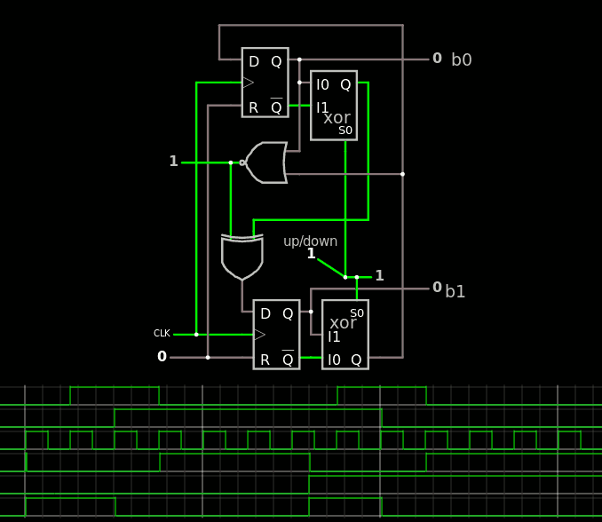
But now we have to alternate from one direction to the other. This implies a 3rd DFF that holds the "direction" level (for now) and some decoding logic.
The b2 output doesn't toggle correctly and can't be fed to the LSB block so the 2 MSB are XORed to give the proper direction.
The FF must have an "enable" input to select when to change the value. This is emulated with the MUX2 in front of the MSB DFF because Fasltad's circuijs doesn't have that sort of gate (or an extensive library either).
The Critical Datapath is 3×XORs and 1×NOR. I'm not aiming at lightning speed anyway.
That's 4 bits now. From there the rest is easy...
To complete the missing bits, another stage is inserted in the middle, reusing all the methods described above. The circuit is epic !
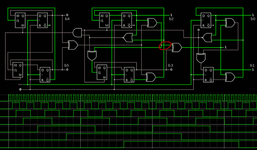
I notice that the system is not perfect yet. The codes are running almost right, as I see some clock cycles are skipped... I'm almost there !
The solution is to rewire one XOR gate to correctly propagate the "direction" signal:
There !
The system is glitchless and modular : it can be expanded to any size, with the LSB, "middle" bits and final circuit with 1 or 2 bits). The CDP is not wonderful (5×XOR: not surprising) but this is not a practical problem in this precise application.
The circuit contains :
6 DFF
8 XOR2 and 3 other boolean gates
4 MUX2 (might be merged into some DFF
And now... VHDL.
20200720 : the source code is now in VHDL/TAP/Gray and works well. It uncovered a really stupid bug in the VHDL gates library which is now solved, and the Gray counters are now also part of the regression tests.
20200808 :
The Gray code is validated in synthesis with Synplify & Libero SOC. However, the circuit must evolve because I'm redesigning the TAP to share the Gray counter with more circuits ! See the log 120. TAP v.2
The circuit starts with buffers so ensure that the fan-in is 1 for all the bits. And since simple buffers invert, the rest of the circuit uses a negative logic and the AND trees are replaced with ORs.
The fanout needs to be "micromanaged" unlike with FPGAs. "Normal" gates are supposed to have a fanout of 1 and some buffers provide x2 and x4 strength, but they invert again...
Apart from the ORs directly tied to the final XORs (which can be combined into AX1D ) we find 2×NOR3, 2×OR3 and 1×OR2. The fanout buffer is merged into the final inverter of the ORs, except where a large fanout (6) is needed : there, the NOR2 has a strength of 2 to drive two buffers with strength 4. The "combined" variant with OR is kept in some places to keep the diagram & code compact.
For the AX1D ( Y=(A or B) xor C, also named xoon21 in the some libraries) the OR is easily merged as a NOR instead of INV of one of the inputs.
Overall, the circuit has grown in complexity, or in fact : better details. There is no use of the new fancy 4-input gates but the AX1D is very welcome... We'll see how the ALU is influenced later !
So I added some extra features to test the circuit easily :-) see INC8_ASIC_test.cjs
The VHDL version was easy to adapt. The first results are nice though are not very nuanced :
The latency is OK and balanced. Most MSB depend on the result of a high-fanout signal, which has been broken into 2 parallel sub-signals. In the grand ASIC scheme of things, that amounts to about 2 gates delays (easily) so it's not inaccurate. Anyway this helps synchronise most MSB as their results arrive at about the same time, with a critical datapath that has been spread/smeared across the circuit.
The first reason is : why did they put the amplifier/buffer on the right, when the left side would have been closer and faster... Is it because of a habit ?
Never mind...
The other reason is derived from the discussion of log 103. NAND3 : I have chosen to use gates with not more than 3 pass transistors in series. This limits my choices to these "First order" gates :
INV / BUFF (x4, x8...)
NAND2 / NOR2
NAND3 / NOR3
The above gate, however, is a "second order" gate : there are 2 kinds of logic operations, as it performs /(A and B and (C or D)), and it still fits within the limit of 3 pass in series. There are 4 inputs now... but it's great :-) Now swap the P and N sides and you also get /(A or B or (C and D)).
Drop one input and you even get /(A and (B or C)) as well as /(A or (B and C)). It seems that /((A and B) or (C and D)) as well as /((A or B) and (C or D)) are on the menu, too, and they are welcome precursors to XOR, MUX2 and latches.
Latches are another critical resource to consider... but so far, the gates zoo is expanding and will greatly ease the "NANDification" of the units. This means I'll have to add these new gates to my gates library, after I checked they exist in the SW-PDK.
So far the "logic vocabulary" must obey these rules :
All inputs have a fanin of 1 : the signal drives only one inverter. This greatly simplifies the load estimates when you read a diagram.
All inputs can have a fanout of 1 : they can drive one single inverter. Logic gates are typically unbuffered. Higher fanouts (usually 4) are managed by ×4 inverting buffers.
Not more than 3 pass transistors in series between a supply node and a gate (as explained earlier).
This means most gates are inverting. If the fanout increases, an external ×4 buffer will re-invert the signal back to "positive" polarity. This reduces the number of gates to consider. And because NOR2 and NAND2 have only 2 pass transistors to traverse, they could be considered as "a bit faster" or "better fanout" (maybe 2).
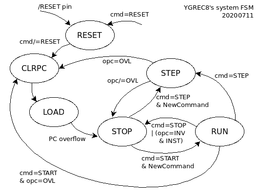
The log 97. Core state machine develops the idea of the 2 concurrent state machines but something is missing: the FSMs don't allow the core to request new code again. This log 20. Automated upload of overlays into program memory describes a mechanism where the code can request a reload of (new) instructions in program memory, but this is not implemented in the FSM.
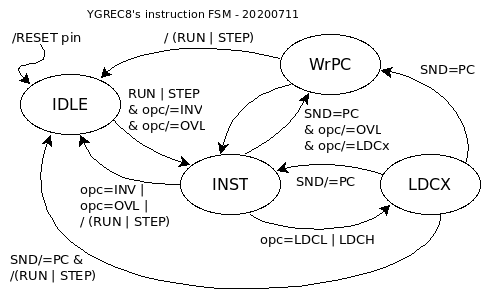
The core has evolved since 2018 and the opcode mapping is a bit different, in particular the MOV and CALL opcodes have changed. However, the OVL opcode is still an alias for CALL (whatever) PC.
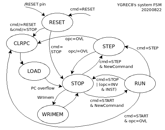
I have updated the FSM diagrams :
The source code is not updated though.
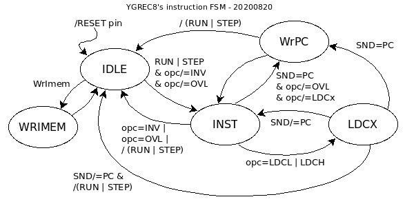
20200820 : I moved to the FSM one problem I had with the eXecute/Slice units, which is : how to cross the clock domains to send a correctly-timed pulse to the Imem block when writing to the program memory. The FSM can do it, but which ?
(at first) it seems the Instruction FSM is the best place to do it.
The core must be in IDLE state for this to work.
Had I chosen the other FSM, the STOP state would be reached through CLRPC & LOAD, which might be unwanted if one wants to selectively load instructions.
But the Inst FSM grows from 4 to 5 states, which can't fit in 2 bits...
Maybe I can engineer a way to go directly from RESET to STOP...
With a new arc from RESET to STOP that bypasses CLRPC and LOAD, it is now easy to send the WrImem pulse from the core's clock domain, AND the system FSM can be removed from the instruction FSM and still preserve the most fundamental properties.
The trick is simple : at P.O.R. the command register is loaded with "RUN", to get the core running, as it would if there was no system FSM. Then the TAP can take over and send other commands.
The command register could even be loaded on POR depending on the status of one TAP input pins (/WR for example ?) since the TAP pins should have pull-down resistors to prevent spurious behaviours.
The core FSM can still fit in 2 bits and the system FSM in 3 bits.
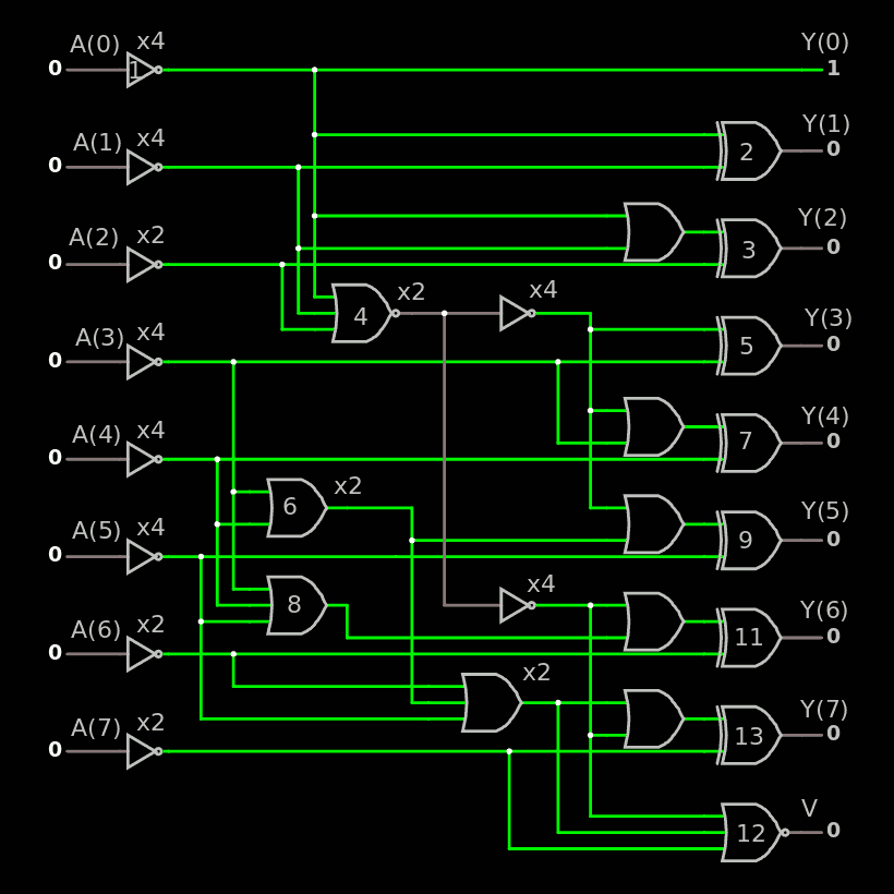
My efforts with Pushing more bubbles, now the carry-lookahead adder were promising but a bug somewhere has made it vain. So I restarted from scratch instead of trying to dig too deep in my own code. That's how I came with the results of Bitslice and now, I have a big advantage : I can have arbitrary polarity of the input and output of the CLA logic and I have more freedom to choose the gates.
Also this time I should make more progressive alterations to the design to catch errors earlier. Like : I should test it bit by bit and build the exhaustive test at the same time :-)
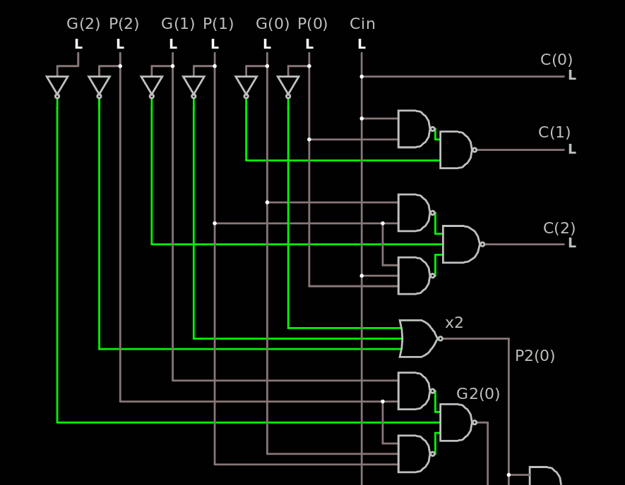
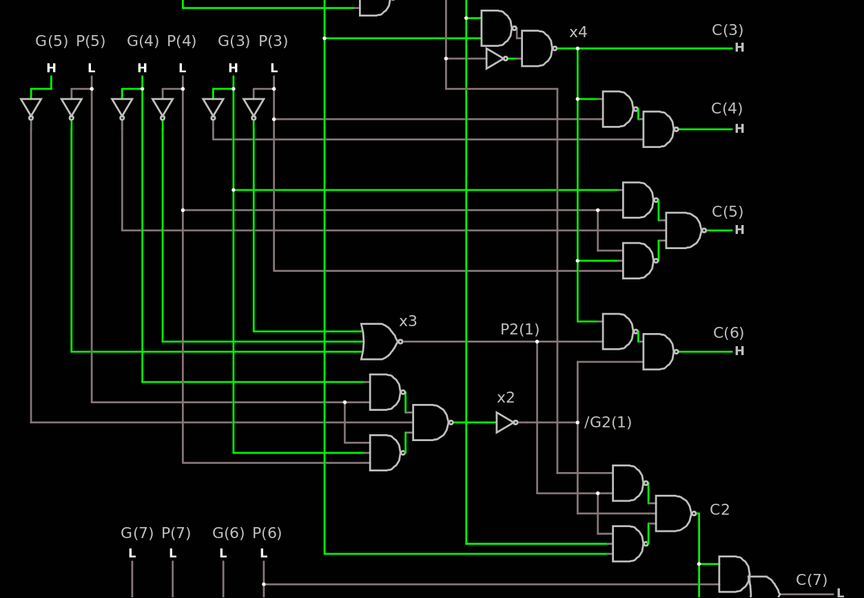
All the G and P inputs benefit from the inverter (which is in fact the output of the NOR2 or NAND2 of the ROP2 bitslice) and they all have a fan-in of 1 so the NOR2 and NAND2 only need a fanout of 2.
The other signals have a fan-in of 2, 2, 3, 1, 2, 0, which is reasonable. Cin has a serious fanout but is ready much earlier so it's not critical.
For P2(0) I replaced the AND3 with a NOR3. This provides the signal earlier than G2(0) because the inverted inputs arrive one inverter earlier (and there is only one driver layer).
The second block of the CLA is quite similar (which is not surprising since it is more or less copied from the LSB part).
The same recipe is applied. The AND-OR is replaced by NAND-NAND, AND3 is replaced by NOR3.
I had to insert two inverters, one on G2(1) because it's used on the inverting input of 2 blocks, so I renamed the signal /G2(1).
All the inverted input signals are used, and only once, just like before.
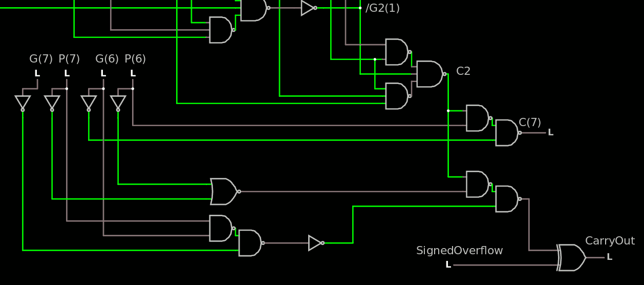
The last bits and the carry output are pretty similar:
Note how each G and P input is used, only once for each polarity.
The gates on the left have some freedom for re-interpretation.
The carry output is XORed but there is no penalty because the other outputs are XORed as well but in the ROP2 and SUXEN level.
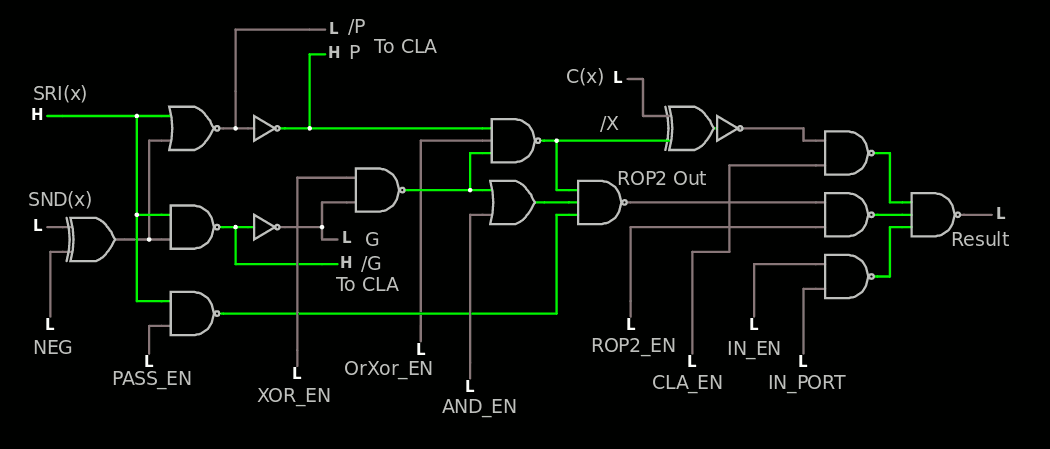
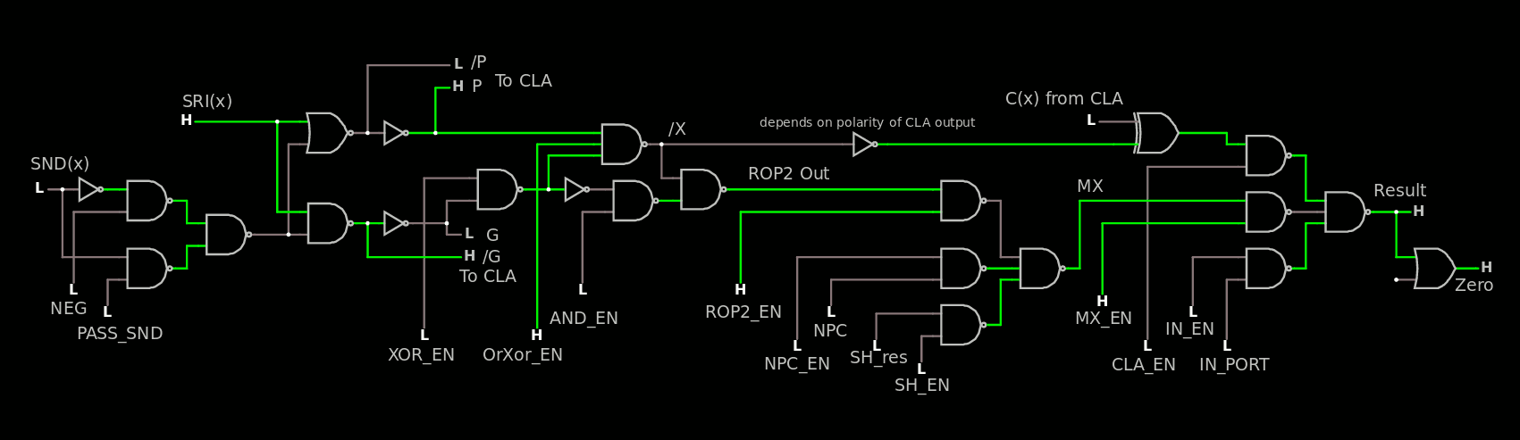
The ROP2 and ALU part has been slowly expanding to the SUXEN but the log 70. The nexus reminds that something is missing : I have forgotten to include PC+1 (NPC) value. So another level of MUX is required, which is fortunate because I had also left the SHL result. I can then use another full MUX3.
and it seems it must be extended a bit with another layer of MUX3 (source)
The CDP of the whole stack is about 10 simple gates and I have not counted the CLA or the IN port. It's pretty satisfying to see that whole "datapath" in one picture, at last :-)
You can see a lonely inverter on the /X signal. This is an optional correction for the output polarity of the CLA. It can be omitted if needed, it's on the "slow path" and provides some degrees of freedom for the CLA design.
Speaking of slow paths : there is one OR just before the ROP2_out signal but it looks uncompressible and not critical so I leave it here. The input XOR for SND is critical though. I'll see how I can reduce the output XOR from CLA, there is a fun trick to play with BJT ("enable" by playing with the CLA_EN signal tied to the pull-up resistor of the interlocked pair).
That's 160 gates for the 8-bits datapath (ignoring the CLA and SH circuits). It looks pretty easy to layout and route but the output and the inputs will be located at the same side to ease routing of the register set. I'll probably move to a 3-tiles high organisation for FPGA & ASIC.
Update :
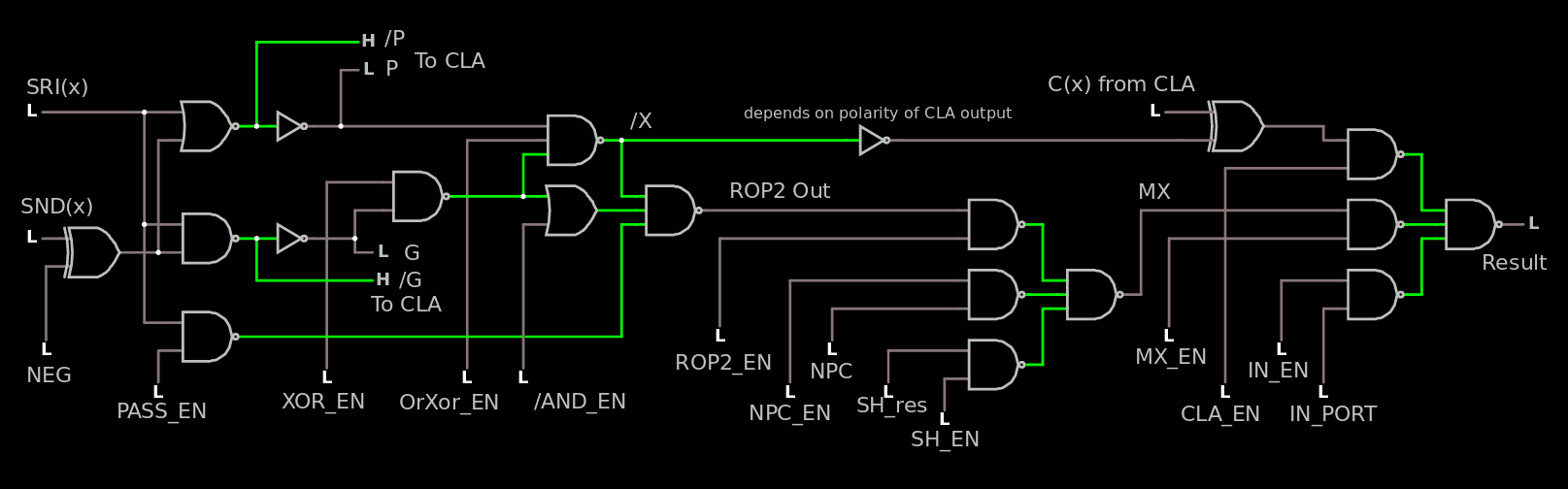
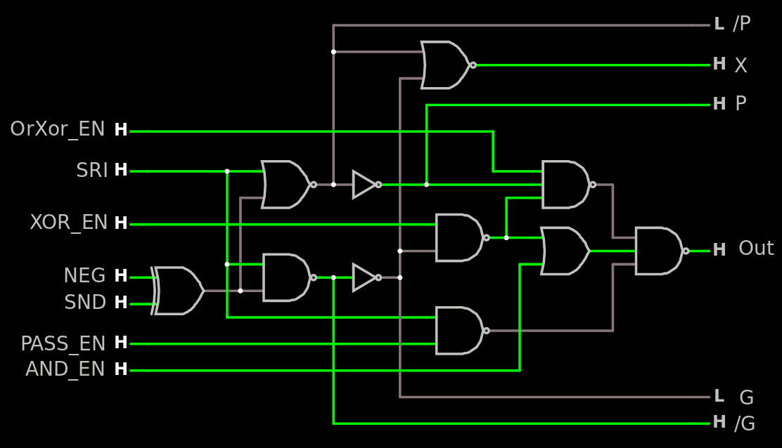
I might have found a trick to save a bit of stuff somewhere :-)
The idea is to combine NEG and PASS_EN at the XOR input level, which saves one NAND2 and reduces the NAND3 to NAND2 (which can also add one more input in the datapath if needed). There is a need however to get /L somehow/somewhere but a XOR contains 2 inverters anyway. But NEG and PASS_EN can be controlled at the decoder level and the other inverter is moved/shared.
Oh and I also replaced the OR (for AND_EN) with a NAND2, one input has an inverter while the other input can be inverted at the decode level. (source)
PASS_EN is renamed to PASS_SND because it makes more sense.
I have also added the Zero detection. That would be a OR8 (in a way or another).
Here we see the signal going from SRI to the Result output, NEG and PASS_SND are disabled so the value flows through the OR logic : OrXor_en, ROP2_en, MX_en are enabled.
In the decoder's logic, AND_EN, NEG and PASS_SND are affected. This removes several "don't care" situations.
     NEG PASS_SND AND_en XOR_en OrXor_en ROP_en CLA_en IN_en MX_en
OR    0      1      0      0       1      1       0      0      1
XOR   0      1      0      1       1      1       0      0      1
AND   0      1      1      1       0      1       0      0      1
ANDN  1      0      1      1       0      1       0      0      1
SUB   1      0      x      1       1      0       1      0      0
ADD   0      1      x      1       1      0       1      0      0
PASS  0      0      x      x       1      1       0      0      1
IN    x      x      x      x       x      x       0      1      0
clear x      x      x      x       x      x       0      0      0
Reader warning : this log/post touches the fundamental things that make me the most passionate about digital design and architecture. Playing with TTL chips, relays and transistors is a fun game but here you have a glimpse of some damned serious matters. This log justifies several aspects of my design choices so strap you belt and learn a few things.
I aim at building the YGREC8 with various technologies (mainly for fun and giggles) but with the same ISA, so the different implementations can execute the same programs, as well as with the same structure and even the same gatelist (except for the relays version). This means that I focus on the manual synthesis of the design and I break down every function down into individual gates. I choose the lowest common denominator for the chosen technologies and then I reuse the same gatelist without trying to overoptimise too much for each target...
This means I must also choose the right structures and keep them (except for the relays). For example, the ALU will be (mostly) identical, with the same CLA because I don't want to re-engineer the system for every new implementation.
The ProASIC3 and the relay versions favour the MUX2 as the atomic, do-everything gate but I intend to use ASIC/CMOS as well as bipolar discrete transistors, which require simpler gates.
Bipolar gates really prefer the NAND function. It's really the simplest, so it should be the fastest...
CMOS ASIC technology loves both NAND and NOR (they are symmetrical) but they have a practical limit for the number of inputs. Apparently 3 is a compromise between size and speed because more inputs would put too many pass transistors in series, which would slow down the gate, or force the channel to be too large to compensate (and increase capacitance).
So the "preferred gates" are NAND2 and NAND3.
Others like latches, NOR, INV and XOR are accepted where needed. For example I have studied the structure of the latches and XOR in several previous logs on other projects (for example the XOR zoo)
Having more inputs to the NAND would be a big benefit to reduce the size and increase the overall speed:
This lets MUX have more inputs and fewer levels, which is better
The carry lookahead (and incrementer) can have a coarser granularity, fewer levels and a shorter critical datapath
and I probably forget a few other units, SHL would be a good candidate as well.
Bipolar discrete circuits can have many inputs, 4 would not be a concern, maybe 8 is possible before running into signal integrity issues. The question is: is it a good choice for CMOS ?
"Multi-input cells are mainly power and area optimization and not performance. Area optimization is trivial due to reduced number of transistors; power optimization is due to the removal of internal switching nodes. I haven't looked deeply in maximum number of series transistors in a design but typically one does not go above four. Going more would need big transistors and likely not that much would be used by synthesis anyway."
Thank you for the context expansion :-)
Let's see how/why this is so.
CMOS obeys to a few rules, in particular t=RC so the goal is always to minimise resistance and capacitance.
Capacitance comes from the gates regions because the thin area where the poly overlaps diffusion creates a capacitor. The smaller the gate, the faster.
However resistance comes from the relative width of the area through which current flows. The smaller the section, the less current flows, so the width must be maximised to make fast circuits.
So there is this basic compromise : if you make a transistor wider you increase the current hence the speed but this also increases the capacitance, which reduces the speed...
And this is for one transistor. CMOS gates need transistors in parallel and series ! And the more inputs, the more in series, and the more resistance, which also reduces the speed...
2-input gates are a bare theoretical minimum for making a circuit. You won't go far with 1-input gates.
3-inputs gates are an extension of the 2-inputs version. Just enlarge the gates a bit to keep speed in check.
4-input gates can concentrate more values but need 2× larger gates than the 2-inputs version to keep the speed. But 2× larger gates also means 2× RC delay, 2× the drive strength and/or 2× the propagation time. A compromise is required such as 1.5× width for about 1.5× increase of delay but this also requires spraying the chip with more buffers/inverters to boost the signals anyway.
conclusion 4-input first-kind gates (NAND4 and NOR4) are good for reducing the power and area (hence costs) but don't help with performance in CMOS. That would however be an interesting option for a power&cost-enhanced version, where NAND4 is preferred every time it's possible. And given today's technology, that power reduction could have great benefits, as AMD found with their latest CPU generations : reducing the power allows you to pack more cores than the loss of individual performance.
Of course it's still possible to plug some 4-input gates at some critical places to "get things done". For example the current SUXEN has a MUX3 and doesn't get the SHL unit. Adding a NAND4 would add the SHL easily into the result bus. Upon closer inspection, PC+1 need to be sent as well so another layer of MUX3 would still work well...
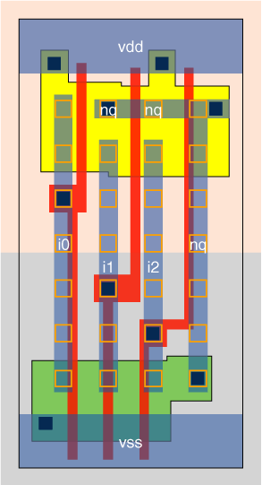
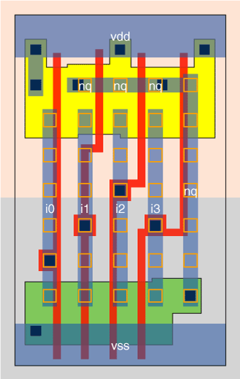
I find AND4 and NAND4 in some standard cell libraries. For example, the SXLIB has NAND3 and NAND4 gates :
The size bloats however when a higher output driver strength is required, with 2 inverters...
However, increasing the number of inputs also increases the density of the control wires and it can increase the difficulty of routing. It's all a matter of balance...
Looking at the above cells I notice that there is quite a significant area that is not used by the diffusion. This could save 20 or 30% of total die area if it was trimmed, with corresponding savings in costs and probably speed. This area is used by more complex gates that need more internal logic layers (XOR, DFF...). So I wonder if/how it is possible to make a "reduced count" gate library with only "low-profile" gates... A sort of "RISC" method applied to CMOS ? :-D
There is still the challenge to disable the output of the CLA so it can be combined by ORs with the rest of the units.
My guess was to decompose the end XOR and include the "enable" signal at the end of the combining gate but I get the wrong polarity. Instead I have this solution for XA1:
however the fanout for the "enable" signal is doubled and this feeds 2 gates with 3 inputs, which uses more space...
It's hard to reduce the XOR gate and each technology has their own tricks up their sleeve to implement it, so I prefer to keep the XOR as is and the output is MUXed with a classic 2-levels NAND circuit:
Now I have moved the final XOR of the CLA back into the ROP2 circuit, which also saves one gate because I duplicated a (N)OR. The final XOR is driven by the "shared XOR" which has a reverse polarity so you can see I added an INV but it can be bubble-pushed in the CLA or in the final MUX as needed. Source:
The truth table is updated :
      NEG  PASS_en AND_en XOR_en OrXor_en ROP_en CLA_en IN_en
/OR   0      x      x      0       1      1       0      0
\OR   0      x      0      x       1      1       0      0
XOR   0      0      1      1       1      1       0      0
AND   0      0      0      1       0      1       0      0
ANDN  1      0      0      1       0      1       0      0
SUB   1      x      x      1       1      0       1      0
ADD   0      x      x      1       1      0       1      0
PASS  x      1      x      x       0      1       0      0
IN    x      x      x      x       x      0       0      1
clear x      0      0      0       0      0       0      0
Simulation with Falstad helped uncover some non-trivial "don't care" states.
The PASS code is back to "ROP2 land" but this shouldn't create too many problems in the decoder.
I added the IN instruction and left the SH codes for a future version, so it fits with the final NAND3 gate.
Some signals such as AND_en are updated because the ROP2_en "shadows" them.
It seems XOR_en and AND_en could have their names swapped ? AND_en is 1 only for XOR, and XOR_en is 0 only for OR...
 Yann Guidon / YGDES