Yann Guidon / YGDES
-
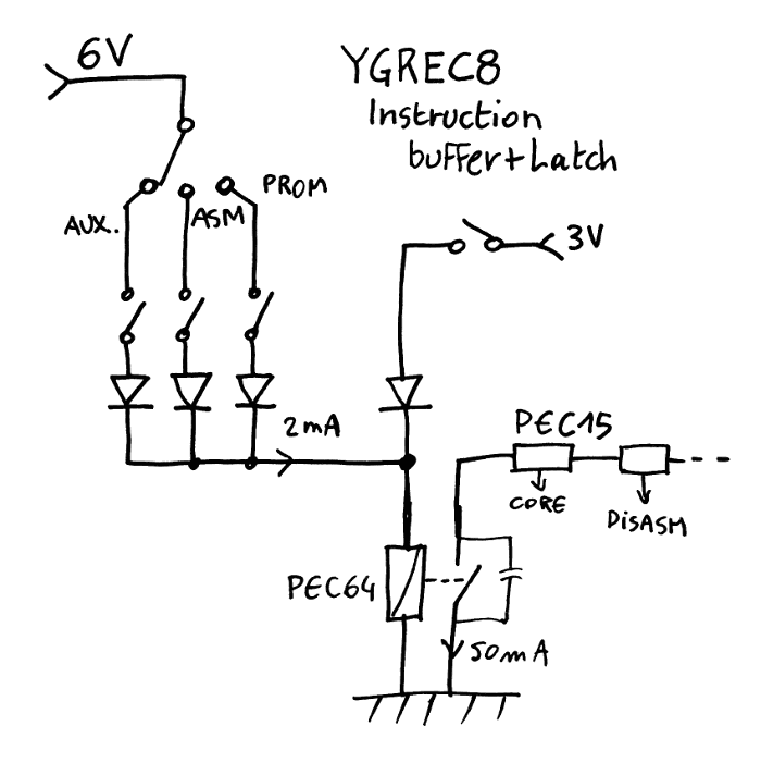
A "hub" for the instructions
10/25/2019 at 20:44 • 0 commentsIn the Y8, instructions come :
- from the program memory / PROM
- from the assembly panel
- from eventual "modern" sources
Then the instruction bits are amplified, eventually latched, and sent to :
- the processor's instruction decoder
- the disassembly panel
- eventually something else such as a semiconductor device...
This is a bit more complex than just plugging things together because all the electrical signals must be at the proper levels...
For now I have built the assembler panel and I start building the disassembler, and I'd love to test them together, but the levels are not compatible :
- The input is a low-current (2mA), medium voltage (about 6V) signal
- The output must be able to drive a string of RES15 coils (50 to 60mA max)
The RES64A is appropriate to buffer the signals and even latch them, if appropriate biasing is enabled.
![]()
The latch feature can be enabled on demand, for example during sensitive phases of the instruction cycle.
Another row of relays can also (dis)connect the RES64's coil from the input, to freeze the state of the processor while the memory and other circuits are in transient phases. The RES60 would be appropriate because it's small and DPDT so only 8 relays are needed, which uses much less room than the other methods. The 16× RES64 will use quite a lot of room, in comparison...
For convenience the latch doesn't use an intermediary capacitor because some operations require a direct connection to the core.
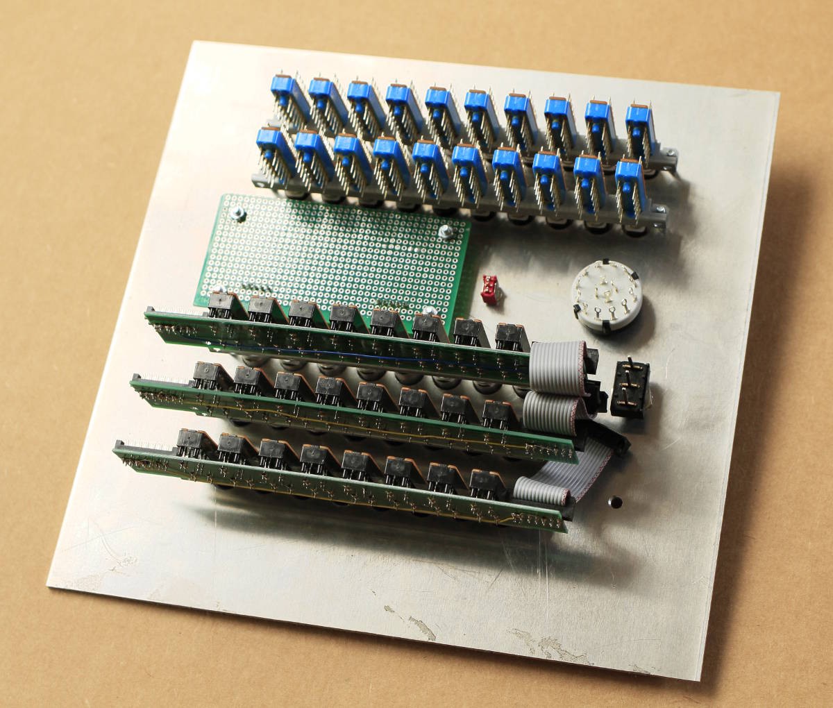
Now I have to find a PCB that can host 16× RES64...
20191118: I drop the idea of the RES60 latches because there must be a proper "instruction register". Program memory can also contain data that must be read by LDCL/LDCH and an early latch would make it harder later...
It also saves some of these precious relays.
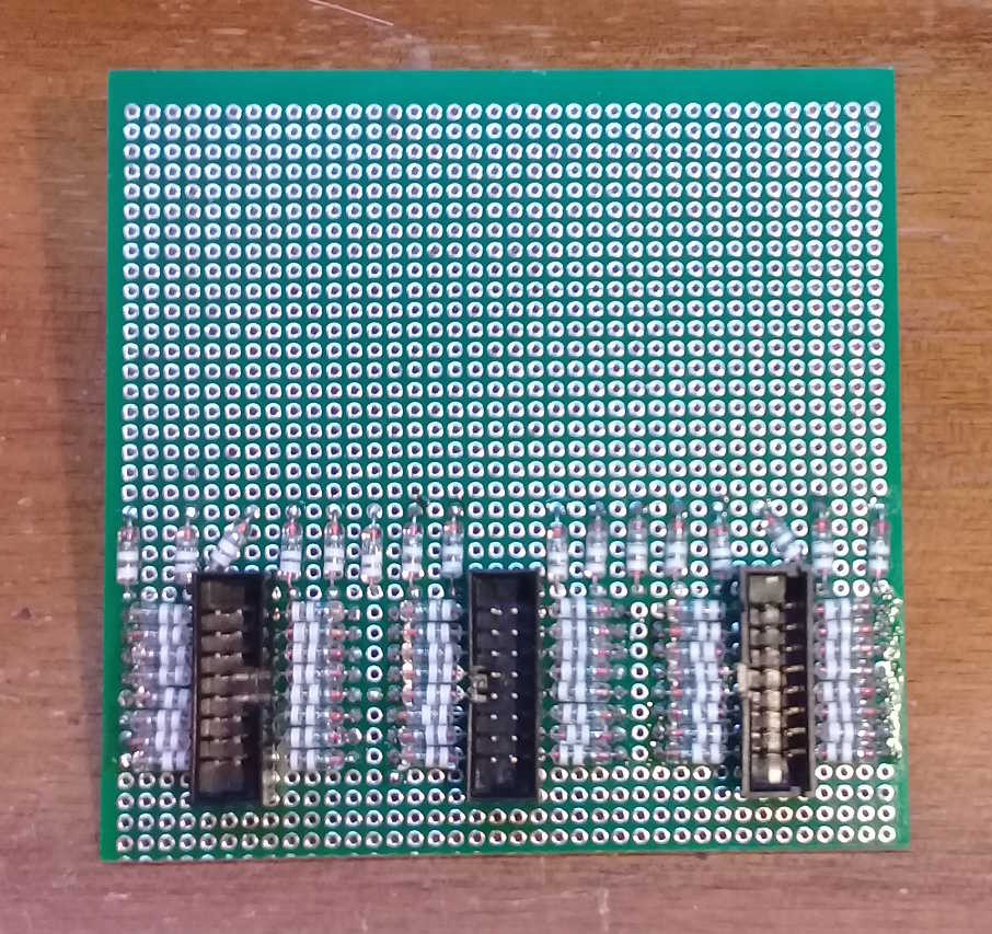
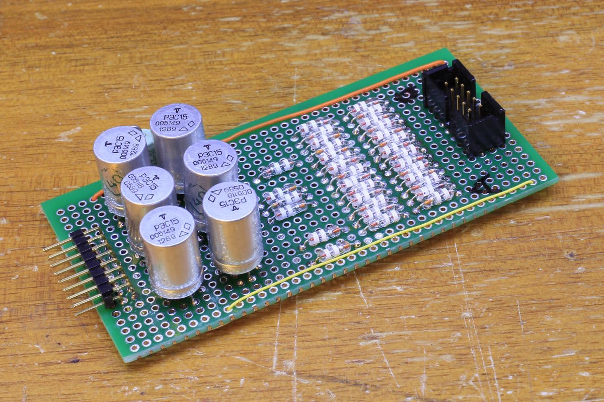
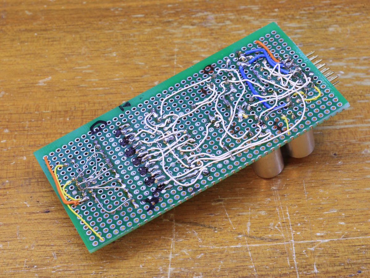
![]()
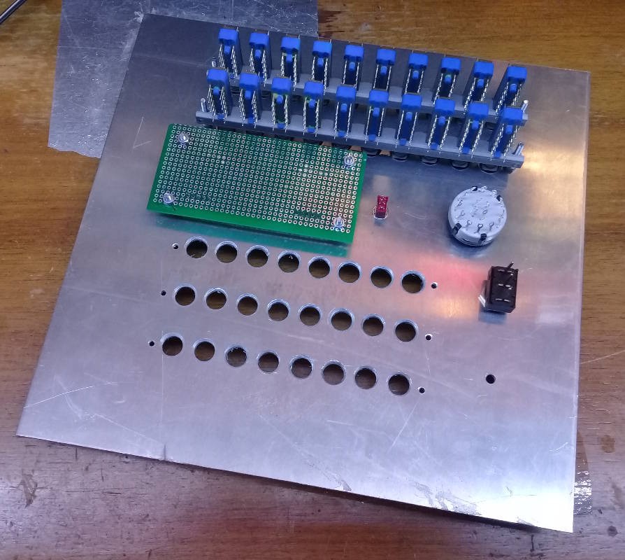
So I started building the hub board on a smaller board, with only 3 connectors and their 48 diodes. More diodes provide the latching for the RES64. The relays will not be placed yet because I need to bin/sort the whole lot and I have not received everything yet. The preliminary data is in the log First plots.
The relays will be placed on staggered positions on both sides of the board to save space, just like it will be for the register set.
Hopefully I'll have some room left in the corners for mounting holes...
-
RES64 > RES15 (somewhat)
10/25/2019 at 03:02 • 2 commentsI received 72× RES64A from Moldova and I'm pretty happy and lucky :-)
@Artem Kashkanov praised the RES55 he uses : the lower current and the higher hysteresis compared to RES15 would be great and I was eager to test something.
The log 86. Sensing relays explored the question of the reed relays and found that even cheap 12V relays from China have desired features for certain circuits of the YGREC8 : mainly as sensors/amplifiers because they require much less current for activation.
I just measured a RES64A and the reference I received is pretty awesome !
- Von : 4.3V
- Ion : 2.1mA
- Voff : 1.7V
The case is pretty bulky but this adds to the charm. With a suitable price, I'd get more of them and use the high hysteresis to build the register set as well.
Even at 2.5mA (worst case), the gain is really significant ! It is less than 1/10 the current required by the RES15 and the hysteresis is somewhat higher, which means : much more stability ! And no need to bin the parts !
Total current : 2.5 × 8 × 8 = 160mA max !
This considerably relaxes the constraints on the power supply, the ripple (and filtering capacitance) is much less and the whole is less sensitive to interferences...
However the supply voltage would be 4.3 + 1.7V = 6V and I'll have to find/design the proper power supply and transformer... But 6 × 0.16 = 1W max !
Now I have to find enough vintage Russian 2K resistors...
There is another change : the RES64 is SPST so it's only on or off... the RES15 is SPDT and can switch the output from +Vcc to -Vcc so it's pretty convenient for the output levels. A register set made of RES64 will require some sort of buffer (maybe another RES64 per bit, so I'll need 72 of them)
-
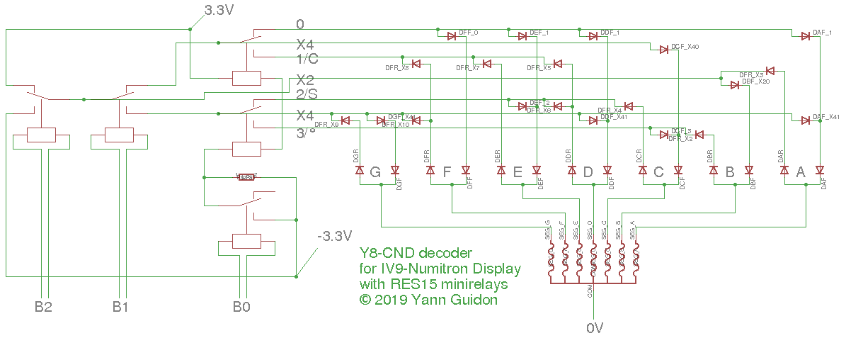
Condition codes : decoder & display
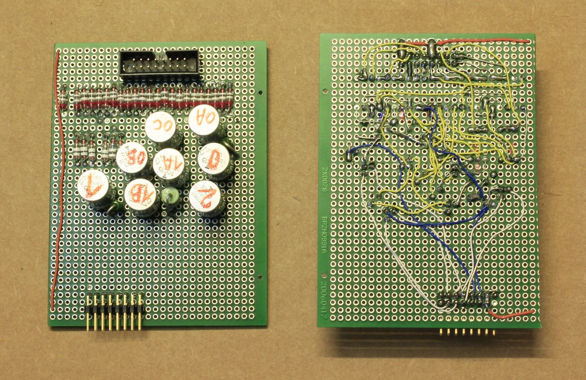
10/24/2019 at 23:41 • 0 commentsThis other module is now OK as well !
What a mess... There were a number of blunders but I managed to find and correct them all.
![]()
The component side is nice but the wire side is ... less nice.
![]()
I somehow managed to swap and invert some signals so it is not an exact copy of the schematics (shown below again for reference)
![]()
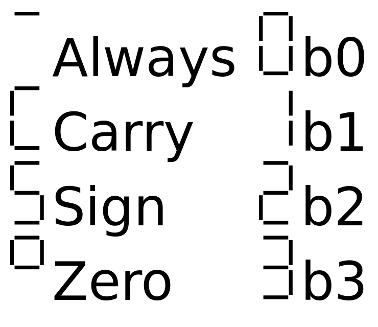
This circuit decodes 3 input bits to the following symbols on 7 segments :
![]()
A 4th bit is inverted with a relay to drive a small Glühbirnchen and signal inversion. Maybe I should also output the "NEVER" condition on the last signal of the connector...
The system is shown and operated in this short video :
I hope you enjoy hearing the relays' clicks :-)
Update :
I also added an auxiliary output to help signal the "NEVER" condition.
However the polarity is inverse (compared to the hexadecimal modules) and can't be displayed on the usual test module.
A reversed diode and a Glühbirnchen are enough but I'll see later how to better exploit this signal (in conjunction with the 4th "neg" bit).
-
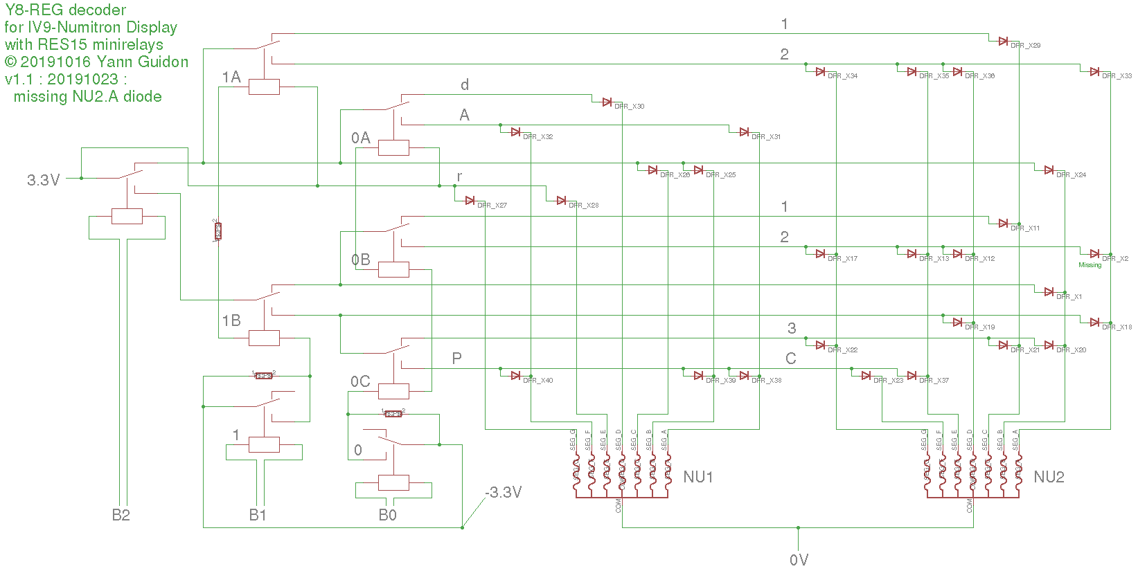
Register name display : OK
10/24/2019 at 17:45 • 0 commentsHi dear reader ;-)
Some pictures would probably please your eyes, I hope you enjoy the sight !
![]()
It was quite some work but the result is nice. The only gotcha was a forgotten diode/segment in the decoder at NU2.A:
![]()
Here is a video of one unit under test :
I reuse the same pinout and test board as the #Numitron Hexadecimal display module for convenience :-)
I'll have to do some "optical design" to prevent glare/reflections and keep the Numitrons readable, but this is for another time. As you see, I use a separate connector for modularity so I can design the front panel independently.
I'm already working on the condition display...
-
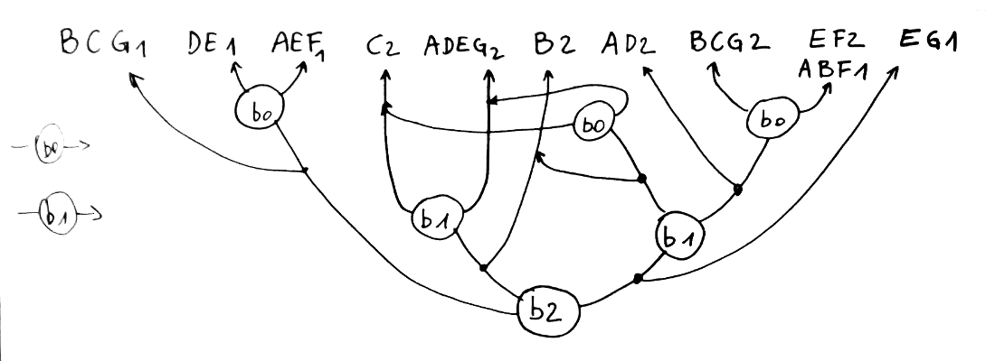
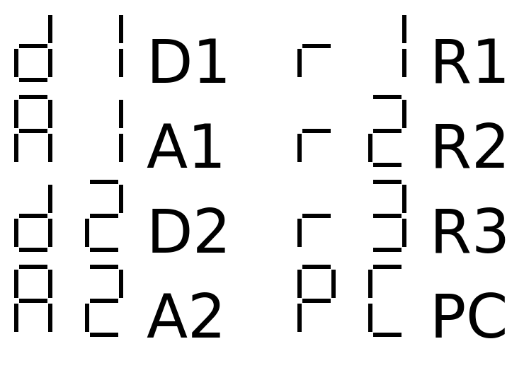
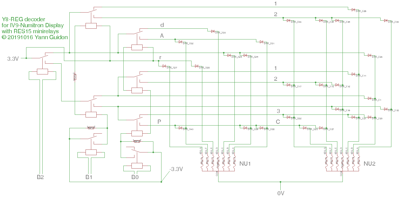
Decoding the register names
10/16/2019 at 02:06 • 0 commentsIn the log Don't go full Numitron ! Unless... OK whatever. I examine how to reuse the techniques developed in #Numitron Hexadecimal display module and apply them to decode all the fields of the Y8 instruction.
For the register name I came up with this diagram :
![]()
This decodes to the following symbols :
![]()
The segments E1 and G1 are always on (for A, d, r and P) so I modified the diagram a bit, later.
I didn't optimise the replicated 1 and 2 because it would make the relay side too complex for little gain (I only have to build 2 decoders). Here is the result :
![]()
To test the circuit, I have built a test device with a "standardised" 26-pins connector and 3 Numitrons. To inject data, I will reuse the connector and pinout of the existing Numitron hexadecimal modules.
Note : the module can be powered down by disconnecting the +3.3V power line. The diodes will prevent shadow segments anyway, even if another decoder is connected in parallel to the Numitron (for example to share the Imm4 and Reg formats).
-
Sensing relays
10/15/2019 at 00:28 • 2 commentsThe RES15 relay is nice but requires way too much current to operate, in particular in some circuits where low current is necessary : the DRAM sense circuit as well as the instruction sense circuit, because 16 bits multiply the coil current, that reaches a value that can't be reliable...
Another type of relay is required and @Artem Kashkanov suggested the RES55 : a reed-type relay with the typical fast operation and low operating current, though at a higher voltage.
I couldn't find a suitable lot of this reference on eBay but found 2 other things :
- RES-64A rated 9-11V : vintage, pretty bulky, only SPST but 2K ohm coil so it must be pretty sensitive
- 1A12 : miniature SIP chinese reed SPST relays, rated 12V, 1K ohm coil, very cheap
I just tested the 1A12 and I am impressed : the contact closes at about 5V (varies with the piece) and opens at about 3V, with a current under 2mA. With such a hysteresis and low power, it even becomes interesting to use them for the register set...
I still have to receive the RES-64A, which would look way better, and I'll have to compare it to the modern miniature version. However there is now a good solution to the problem I had before : I can switch 16 bits on, and draw at most 2×16=32mA, which will not strain the address decoder's contacts much.
Oh and I still have to design that automated relay tester...
-
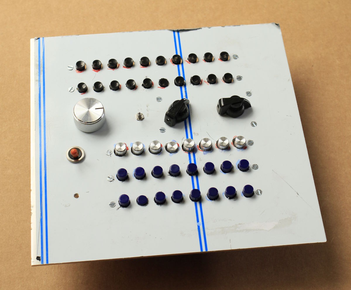
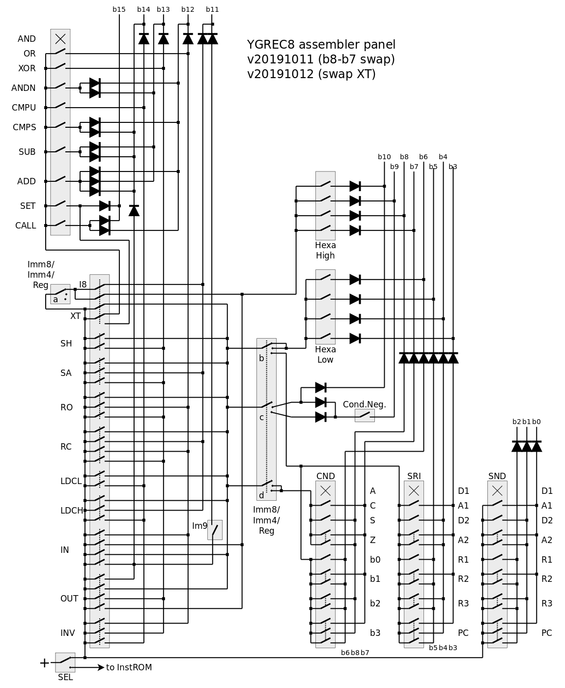
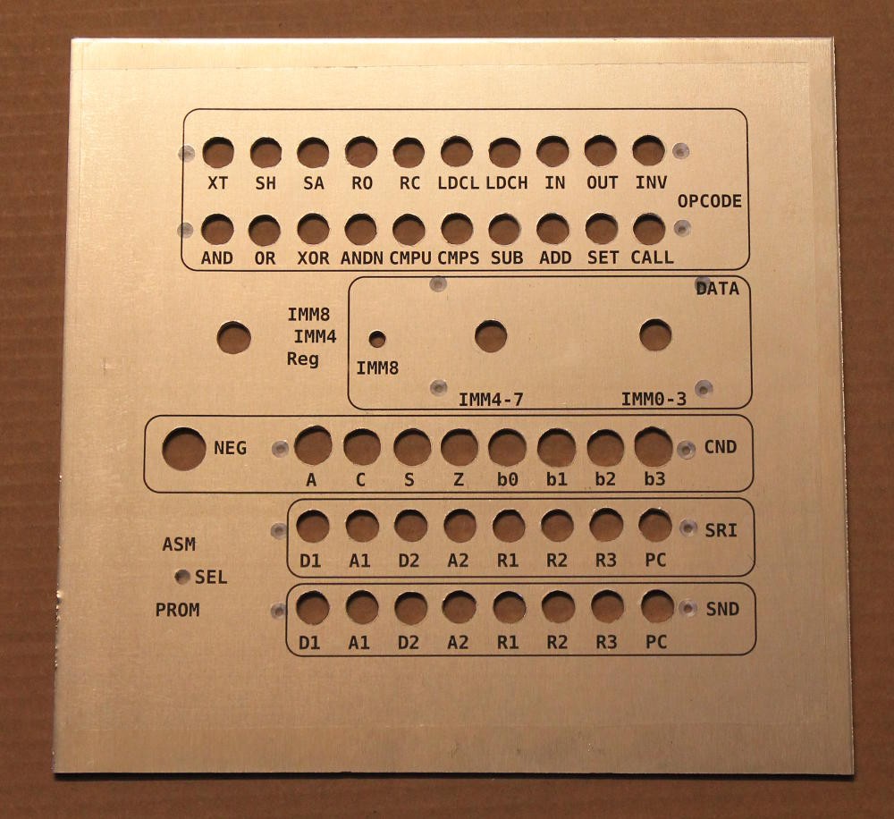
Assembler panel working
10/12/2019 at 23:23 • 0 commentsI made it !
I had to correct a couple of blunders (see the diagram below) and now the system woks (almost) as expected !
![]()
Not all the forbidden/impossible codes are prevented :
- IN and OUT seem to allow the IMM4 and REG modes, though the output binary code will be decoded "correctly"
- INV allows SND to be output
- probably some other obscure combinations are possible
However this panel is only one half of the ASM equation : the disassembler display will prevail over the buttons configuration.
This is why some markings are missing : when programming, look at the output and trust the display, don't stare at the buttons.
.
.
(I'll have to shoot a video...)
.
.
-
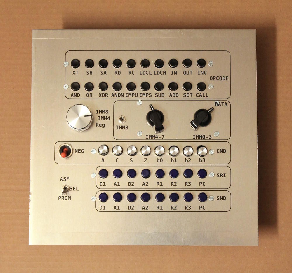
More progress with the assembler panel
10/06/2019 at 15:07 • 4 commentsIt took a long while, efforts, expenses, and a full disassembly of my laser printer but here it is !
![]()
The look/aspect is great ! I had some little issues with the size (maybe due to slight resizing somewhere) and there are a few hicups with some mounting screws.
However the toner ink sticks rather well to the vinyl sheet and glueing didn't leave bubbles. The alu face plate can remain (mostly) clean and it adds a lot to the ergonomics :-D
Locating the "right" plastic sheet took a while...
And here it is in all its glory !![]()
All the switches are soldered but the assembly/wiring is not complete, I need to add another board to really get all the signals together. So I created a small board with 16 Glühbirnchen to ease the tests :-)
-
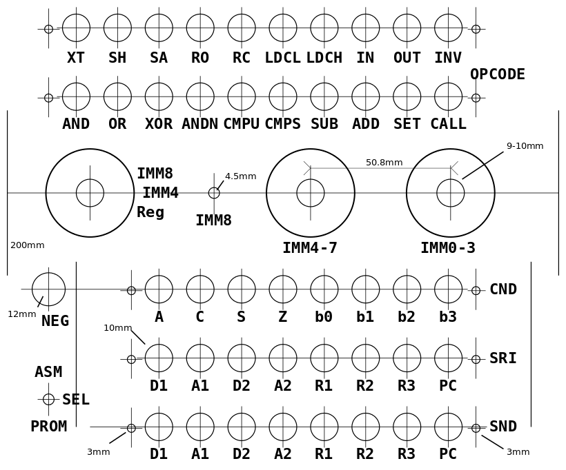
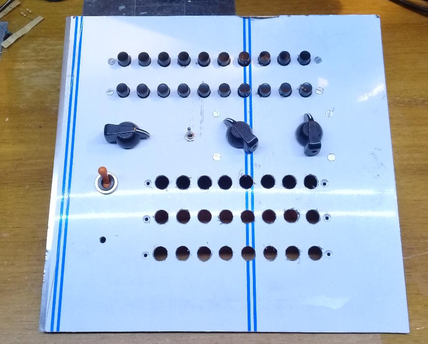
Progress with the assembler panel
09/29/2019 at 05:26 • 0 commentsI tried to fight procrastination and while it's fun to prepare, gather the parts and imagine things, implementing is still important, despite the higher efforts... I think I solved most of the issues so I decided it was about time for action, instead of starting yet another sub-project :-D
One part (the ROM/ASM switch) is still missing and might be delivered late but it is not essential and it can be added later. All the other switches are here so let's go !
![]()
I have uploaded the DIA files for the layout of the buttons and switches. They are laser-printed on normal paper, which is then glued (with a glue spray) on a suitable aluminium plate (found in my archives). So far the expense is about 8€ for the glue spray :-)
![]()
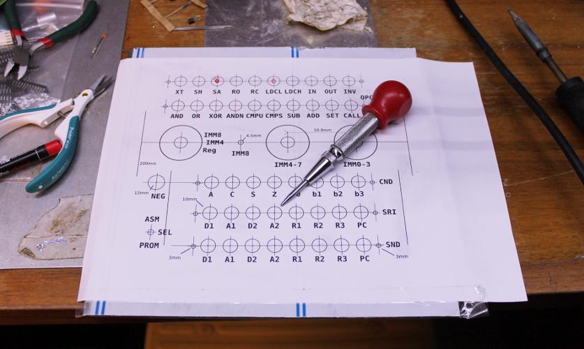
Once glued, the centre of each hole is punched to help later with the drilling.
Drilling took "some time" because of the required precision and odd diameters but my neighbour Alex greatly helped ! Thanks dude ;-)
Overall, the result is surprisingly satisfying and close to my expectations :-)
![]() The action of the buttons is great and I did my best to not make it too compact, which also helps for the wiring on the other side :
The action of the buttons is great and I did my best to not make it too compact, which also helps for the wiring on the other side :![]()
The two hex encoders don't have the appropriate nuts and can't be fastened to the alu plate, so I made a mezzanine PCB, which will later host diodes as well.
The 3 lower rows of buttons have some alignment issues and need filing and adjustments, that's more work but the rest was almost smooth :-)
Better pictures :![]()
![]()
Nothing is wired yet : I need a way to "laser print" the marks on the alu plate.
-
Project organisation
09/10/2019 at 23:24 • 0 commentsPeople are (rightfully) confused with this project, and I understand why: it's ambitious and covers many aspects at once.
For other projects, I have split the whole project into several sub-projects, for example into an architecture ( #YASEP Yet Another Small Embedded Processor) and various implementations ( #microYasep, #Discrete YASEP...). Even for the precursor ( #YGREC16 - YG's 16bits Relay Electric Computer/ #YGREC-РЭС15-bis) I created several sub-projects ( #YGREC-Si , #YGRECmos, #YGREC-ECL... ) that clearly separate the architecture from the various technologies I wanted to explore.
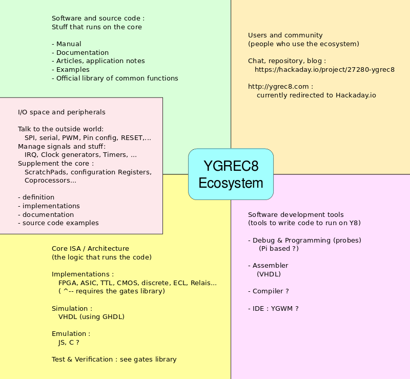
But designing a new microprocessor is more than defining an ISA and making the prototype work: it's a complex ecosystem that must be carefully crafted and every piece of the puzzle must fit right into place. I think that the following sketch give a taste of the ambition of the project :
![]()
In fact it's not so much different from the YASEP and F-CPU, except that I can go deep in the design of everything, thanks to the simplicity of the core.
The immediate use of Y8 would be as a softcore in FPGA projects where a tiny but easy-to-use and expandable microcontroller is required. However getting there also paves the way to more sophisticated cores and technologies...
I admit that at this moment, I focus mostly on the ASIC and relay implementations, which hold the whole project back and I need to progress on other fronts. However some tools (such as the #VHDL library of ProASIC3 gates) are in development and should be short-term only, but are very important for the rewrite of the core in VHDL.
Stay tuned...
YGREC8
A byte-wide stripped-down version of the YGREC16 architecture
 The action of the buttons is great and I did my best to not make it too compact, which also helps for the wiring on the other side :