Sadly, DFF (the normal gate that samples the input data when the clock rises) are silicon hogs. It will depend on your PDK and SCL of course but one DFF is two transparent latches (unless you use the Earle topology, which has been abandoned).
These DFF gates are essential and need to be used all over the place but many circuits do not require them, yet your HDL coding habits will lure you into implementing more and more. For example certain control/configuration registers, IO ports, and even the register set can be shrunk (which also draws less static power and saves silicon real estate)
Of course if you play with FPGA, the DFF are "free" and this won't make a difference, until you port to ASIC and your floorplan with explode: what was free now costs 4× or 6× more than a normal boolean gate.
4-phase clocking can be used for long pipelines (multipliers ?), if the circuit can be cut into 4 equal-time slices.
And this applies to "standard CMOS", as Domino logic rewrites all the rules (but you're unlikely to encounter this unless you work for the biggest companies)
Let's start with a little reminder of the instruction lifecycle.
Decode is when the instruction has been fetched and selected, stored in an instruction buffer or similar, and the fields are broken apart to decide what to do.
Emit is quite synonymous with Issue. It is when the instruction's parameters enter the execution pipeline to start the read op / operate / writeback dance.
Commit is when it is decided that there is no "going back", the instruction will keep its slot in the pipeline and will not be cancelled (think delayed slots or conditional moves as some examples).
Retirement is specific to Out-of-Order CPU core : the in-flight instructions are retired from the reordering buffer to restore program order and update the instruction pointer. It does not contribute to the operation but preserves control flow consistency. This is equivalent to commit, but pushed beyond the execution pipeline.
The semi-radical and first F-CPU architecture called FC0 used a principle borrowed from common sense and the CDC6600, called "Out Of Order Completion" : instructions are emitted and executed in order but since some take longer than others, they can writeback to registers in a different order than during decode. Other instructions can be scheduled by the programmer/compiler to use other resources until the late result becomes available. It usually requires a "scoreboard" that (if done correctly) uses much fewer resources than classic OOO. The performance is less aggressive though and depends on smart scheduling of the instructions. Which is a fair compromise for any RISC endeavour.
Of course, memory accesses can stall, trap and who knows what, so FC0 introduced weird load/store instructions that then became the fully architecture-visible address registers of the later YASEP and beyond. These "split" instructions decouple the memory units and shield the main blocks of the CPU (decode, execution and memory) from each other. This fits very well with OOOC.
To design the FC0's ISA, it has been decided that a decoded/emitted instruction can not be rewound back or cancelled/bubbled. This would create a nightmare of register renaming, issuing and retiring that might bring 20% of performance but increase the size by 100% at least, and testing/validation become worse.
Then there is the SPECTRE class of attacks that play on prefetchers, speculative execution and other dynamic states. FC0 came long before this was a major recognised threat, but the DEC people had already spotted the danger when designing the OOO Alpha 21264.
Furthermore, typical OOO cores require branch prediction because the pipeline depth is seriously increased, sometimes ridiculously so : an ALU operation would be one cycle among 7,10 or 13-cycle deep pipeline. For the same size you get two in-order-emit cores and twice the branch decision throughput without the hassles of a huge branch history table, you can even multithread/multiplex the threads.
All in all, if you want to have the best ever performance for a single thread, you'll pay the price in pure cost, surface, complexity, vulnerability... Of course this also shields the programs from whatever architectural idiosynchrasies and OOO cores can vary in any way possible with little loss of performance.
But if you want to KISS, stick to "Emit is Commit" : any instruction that enters the execution pipeline (operand read, operation, writeback) is valid and will complete with no chance of trap. This forces the ISA to make all instructions conditional to their execution being legal, and the operands to be ready: a scoreboard does that. FC0 also keeps hidden flags to tell the decoder that a read from memory to a register is complete, so the instruction decoder may stall.
This simplifies trap handling and pipeline flushes considerably since there is no specific pipeline flush mechanism, and the pipeline can remain shallow, which highly reduces the need for a branch predictor.
I think the "original sin" in the early 80s was the early RISC CPUs that included data cache lookup inside the pipeline, making it vulnerable to flushes upon page fault. Load/Store operations were efficient back in the day, until the balance between core and memory dramatically changed.
.
Here are some replies for Duane :
OOOC (à la CDC6600) can complete/writeback instructions out of order because the operands are all available and the result will update the scoreboard during writeback. This will then provide the operand for other dependent instruction, whatever the operation's latency : a typical example is ADD vs MUL, which allows some code scheduling tricks described at http://ygdes.com/dct_fc0/dct_fc0.html
(For now I will skip the issue of having to write several values back simultaneously in the register set)
OOOC does not care about the actual latency of the operation : we can simplify the system when all the latencies are fixed (like 1 cycle pour ADD, 4 for MUL...) but the scoreboard system can handle variable latencies, for example a word that must be fetched from L1, L2 or external bulk RAM. This also includes page table walks. But the PT lookup could trap.
.
Overall, if we apply the TTA (Transfer Triggered Architecture) principles,
Classic OOO performs the opcode "retire" at the end of a large buffer of in-flight instructions (with a HUGE dependency on the branch predictor's efficiency)
OOOC folds the "retire" part at the decode stage, and can solve branches way earlier
.
More about LOAD/STORE instructions:
Although the canonical MIPS archi makes them trivial, they are not at all. In fact their operation could almost be microcoded in the edge cases (RISC such as early MIPS and Alpha use actual privileged code for this).
More recently, OOO cores split the STORE instructions into 2 µops, one for the data dependency and another for the address dependency.
FC0 uses a split scheme where a LOAD or STORE instruction overlaps the next access. - The first part handles data writeback : the decoder checks that the pointer register is ready and has a valid flag, then (if it's ok) writes the destination register (or reads the source register) with the associated value. - The other half computes the address of the next operation and performs the checks (L1 cache available, page table entry found and valid...) which does not trap : it's a sort of "prefetch".
Overall, it "looks" like a classic load or store instructions but the opcodes can trap early, at decode time, if the previous load/store using that register has a problem. That was considered as a "reasonable compromise" to the compiler people who didn't want to go out of their comfort zone, yet this abides to the "Emit is Commit" mantra.
All of my later archis used pairs of address/data registers and dumped the load/store instructions altogether, considerably simplifying the execution and decoding units. The system is close to the CDC6600 except I don't use separate write and read registers (which may or may not be optimal, it's a separate discussion). The program starts with writing an address to the address register, triggering an address lookup and TLB check. The next instruction that will write or read the linked "data" register will be locked by the scoreboard until the situation is clear : the status of the data register will go from "pending" to "OK" or "Trap" so the decoder does not emit-and-commit the instruction that uses the result of the data register as an operand for a new operation for example.
"Emit Is Commit" also applies to other control instructions, such a IO or privileged operations. But LOAD/STORE is a pretty wicked case.
.
Note:
One exception to the rule is the UMIN/UMAX/SMIN/SMAX instructions where the 2 operands are subtracted and the ALU's carry output disables the writeback control signal. This is a small hardware change that replaces 2 instructions (and more cycles) with almost no side effect (except for the bypass logic)
.
Thanks to Duane Sand for forcing my foggy brain to make clearer explanations.
The title says it all but a deeper explanation will shine more light on it.
This is another point where I diverge from the Patterson & Hennessy canon, which emphasises the study of real-life code to see which opcodes are the most used. This was a major argument in the 80s when the RISC vs CISC debate raged, and we should not forget that at this time, most computers (microprocessor-based or not) were microprogrammed (let's exclude Cray's designs of course).
Reducing the instruction set complexity also reduces the weight of the microprogram, which has almost vanished by Y2K (if you forget the x86 of course). So today, when you create your own ISA, you look at the "Quantitative Approach"'s figures and should ask yourself :
Does this apply to me ?
Is it my relevant to my application or domain ?
What is the effect of the compiler ?
Haven't times changed since ?
P&H's RISC works (and their predecessors) have a very good point against microcode, which has been cemented during the last 40 years. But this argument has sometimes been taken to the extreme, creating weird feedback loops.
Let's take C: it was designed on a PDP-7 then PDP-11 and inherited some features of these platforms. In particular the absence of rotation operator. And there are only the AND/OR/XOR/NOT operators. So what did the RISC people do ? They found that none of their benchmarks (written in "portable" C) would include rotation or combined boolean operations. So the SPARC and MIPS didn't have one.
My point is : if you already have a barrel shifter, you can do rotation with a small additional work. The counter-argument is "it will slow down the whole pipeline for an operation that is barely used and can be emulated with 3 instructions" (if not 4). Now, when the codepath reaches the point where rotation is important, these 3 opcodes slow the tight loop down, increase the time and energy to move data around (in and out of the register set etc.) as well as the register pressure (to name a few).
OK maybe that was not the perfect example, let's look at the boolean operations: there is a whole world beyond AND, OR and XOR. Particularly if they are integrated in the ALU where the adder needs one operand to be inverted to perform SUB. This inverter (alread covered in other logs) can be reused to perform ANDN, ORN and XORN. A bit more fiddling gets you NAND and NOR, for almost no real penalty in clock frequency. And yet these are not implemented.
Intel brought ANDN with the Pentium MMX and the full ROP3 set in the latest Core generations so there is some merit to it right ?
But the common languages (and C at their roots) does not provide these operators, which must be inferred by the compiler, leading to the underuse of these opcodes.
These are only 2 examples but more exist. Thus
When an operation provides more options for marginal overhead, expose them at the opcode level. Languages and compilers may ignore them but when you need them, you'll be happy. This is why I provide ANDN with the YGREC8 and the whole ROP2 in the YASEP. The cost of these "extra features" is anecdotal and the times it will save your a$$ will be less remembered than when you miss them.
Because remember: it's a different case than the one against microcode. And don't let others tell you what you don't need.
This is not just so it could run FORTH almost natively.
This is a HUGE safety and security feature.
Plus it also helps performance by separating accesses to different memory regions, while restricting access to the control flow structure (reducing the attack surface).
The call stack should be almost inaccessible to the lay program.
More than one data stack is welcome but not necessary. And another type of stack would be for error handling.
If there is anything that fueled the RISC vs CISC debates over the decades, it's the status flags, and among them, the carry flag is an even hotter topic.
This flag has been a common feature of most architectures and MIPS slashed it. Considering that only ASM would support it, it made sense, in a way, because implementing it would not significantly improve the overall performance. After all it's a 32-bit architecture so multi-precision is not required, right ?
Looking at the shenanigans required to implement multi-precision additions on YGREC8 (5 instructions and 2 branches) and the end-around-carry in C for PEAC (or: "wrestling with GCC's intrinsics and compiler-specific macros"), the carry flag is not a done deal. The POWER architecture implements a sophisticated system to get around hardware limitations but nobody seems to have caught on it.
There is a big problem as well: the high-level languages. This can't be easily fixed because this side is so deeply entrenched that no solution is in sight. We end up with hand-coded libraries for multi-precision numbers (gmp ?), non-portable macros, weird intrinsics, platform-specific code...
Platform-wise, there is no easy solution but it is not hopeless.
Not all architectures need to avoid the carry flag, in particular microcontrollers or cores that will not grow to the point of using out-of-order.
For Y8, the opcode space is so short that I had to ditch the add-with-carry opcode. This is replaced by a 5-opcode macro (10 bytes instead of 2) whenever needed. We'll have to deal with it. (update : this and other issues made me add a "prefix" instruction, turning the RISC-like archi into a multicycle core)
The YASEP has a larger opcode space and includes add-with-carry and sub-with-borrow. This is very classic here.
The F-CPU however is a totally different beast. Not only can't it have a single carry flag (due to the split pipelines), but because it is an inherent SIMD architecture, several carries would be required. There, the idea is to use a normal register to hold the carry bit(s), using either a 2R1W form or a 2R2W form (ideally).
2R2W is conceptually best except for the need to write 2 values to the register set at the same time. Each partial carry gets its own place in the register in SIMD mode, and there is no bottleneck for the single carry flag at the decoding stage. The single opcode works in a single cycle. FC1 could write the extra data to another cluster. Eventually, the opcode could be a two-cycle instruction, first delivering the sum then the carry on the second cycle.
2R1W splits the operation results in 2 separate opcodes, while only one operation is performed. It is slower because 2 successive opcodes are required but it is an easy addition to any existing ISA. On the programming language side, an extra operator "carry" (probably @+ and @- ?) can do the trick.
There is no perfect solution. Each type of core requires a complex balance so as usual, you're the one who decides (and is to blame).
Log 27. Tagged registers talked about "hidden"/"restorable"/"implicit"/caching tags.
There is another type of register tag that is explicit and directly interacts with the ISA, the programs and their state. In this case, the goal is to move the ever-appearing size and SIMD flags of many instructions, to the register set.
This saves at least 3 bits from every instruction so this is a great win in general-purpose processors like #F-CPU. This is less an issue for YASEP and YGREC8 which only deal with single-size values.
However the side effects easily counter-balance this easy win. Trap behaviour must be clearly defined and consistency checks must be sprinkled all over the system.
A simple instruction/opcode like ADD then has many behaviours, depending on hidden values : integer or FP ? scalar or SIMD ? what size ?
The behaviour is not apparent from the opcode alone and we can't know which unit(s) to use at decoding time.
OTOH tagging the registers could be a "cheap and dirty way" to extend an ISA while reusing opcodes with mixed data.
Don't have instructions that can run only in certain "modes".
I know many CPU do it, even RISC-V, but I can't find a decent reason to accept this.
It's a slippery slope : you'll want to do more and more.
It's a waste of instruction coding space, which also reduces the overall coding efficiency.
It increases the decoder's complexity.
What does an instruction do that the Special Registers can't ?
Remember : Special Registers are where all the configuration, and protection, occurs, so there should be only two instructions that enforce "capabilities" : GET and PUT. They, and only they, clear the pipeline and ensure serialisation, trigger a trap/fault if the address falls in a forbidden range.
The SR space can grow while keeping the very same management opcodes. You don't need to change the decoder if you add features, it's all in the SR circuits.
My choice follows the classic SIMD Intel instructions, when 2 bits are available in the opcode (such as the #YGREC8) :
AND
OR
XOR
ANDN
The last one is combined with AND and OR to create a MUX2 function for example.
When 3 bits are available, like the #YASEP, I add the remaining ROP2 functions:
NAND
NOR
ORN
XORN
There are 16 combinations for 2-inputs gates, 8 of them are "degenerate" (output if 0 or 1, or A or B or /A or /B, or a swap of inputs for ANDN/ORN).
With the full 8 functions, any significant boolean calculation becomes possible and efficient. This is particularly useful for "lateral computations" such as #ANGOLA - A New Game Of Life Algorithm or even some particular implementations of crypto algos, where the LUT sequential lookups are replaced by parallel boolean computations.
When you start to design a computer, you usually start with rule 1. Use binary, 2s complement numbers (unless you're @SHAOS or @alice crush) but it's only the beginning. You have to choose a technology, which is a complex entangled web of compromises and constraints.
cost
speed
size
space
availability
power consumption
interfacing with other stuff
what's new/fun/enticing/trending
Of course,
if you use vacuum tubes, integrated circuits or FPGA, the rest is mostly moot due to their inherent properties.
I also assume you're not going anywhere near #Diode Resistor Logic either, though you might find inspiration here.
Relays have a great range of "topological expressiveness" that are worth a whole article.
In fact, from here on, I guess you'll use discrete (MOS)FET or BJTs and things get downhill from there.
Many Hackaday projects, and in particular the #Hackaday TTLers, love to explore and play with various ways to interconnect discrete transistors. It's just a notch below the thrill of designing an integrated circuit but way above that in the BMOW wow-factor. You can touch it, probe it, fix and patch it, show it off and impress...
Creating a logic gate is an art in itself (ask Harvey about it), which draws from both boolean arithmetic and small-signal analog design, and we can dig in the literature, in the past or in the present, to find inspiration. Where each "logic family" differs is what they can express and how they perform each function. The range of possible functions is a sort of expressiveness, and this also deeply influences your higher-level design, as well as design methodology.
This page is important because it gives you a taste of how miserable you will feel, once you get a few working gates. For example, if too few inputs are possible, the final circuit will be slower because of logic fan-in restrictions: for logic reduction, a 2-tree uses more stages than a 3-tree, and a 4-tree is faster, but might each gate might be slower, so you must find a balance somewhere. One typical example is how you design a XOR gate: it might cripple your critical datapath and speed if your logic family is too limited.
The basic gates provide NOR and/or NAND, which I call "first order gates" because there is one level of inversion. Along with the MUX2, these are the "most basic gates" from which you can build all other circuits, but MUX2 is cheating because it contains both inversions, OR and AND. Building a computer with them is possible, but still a challenge ! You have to turn everything into a sequence of NOR or NANDs. This is why "expressiveness" is so important for architects and circuit designers : some families offer a wider range of gates that make life easier, critical datapaths shorter and circuits simpler.
Another choice or constraint is your ability or willingness to use complementary transistors. If all you have, or can get, is a single type, then you are more limited in the possible topologies and you are forced to perform more boolean trickery with the few possible gates. OTOH if you can source both P and N types, you can exploit both NOR and NAND, or combine them in creative ways that could reduce both complexity and power.
But mostly you end up with NANDs and/or NORs... you have to choose carefully !
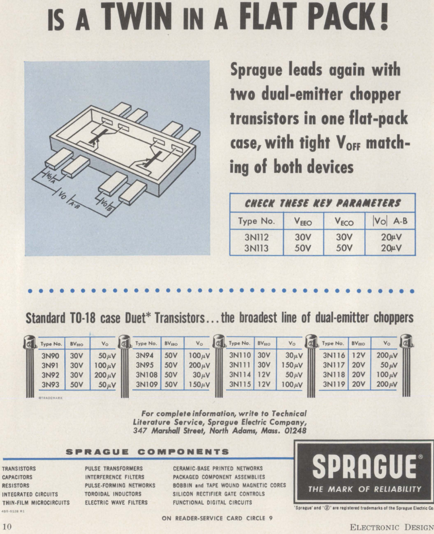
Chances are you'll want to try your hand with a proven and reputed family : TTL, the one and trueTransistor-to-Transistor Logic. One transistor per input and one for the output sounds reasonable and the basic gate is the NAND, such as the 74x00.You notice the weird transistor, which briefly existed in discrete form half a century ago. You can substitute a pair of classical transistors (tripoles) for each of them, which is mostly irrelevant in a digital design (unless your parts are really badly binned)
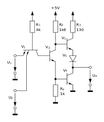
You can't go wrong with such a classic but soon you'll be trying to get more performance with Baker clamps or speedup capacitors. Oh and you can't find discrete transistors with multiple emitters. In the end, the speed will also be limited by R2 because the pull-up transistor has to fight the load's RC. Decrease R2 and your speed is enhanced at the cost of the dissipated power, or saturation problems. If you want to go even faster, you must use totem-pole or push-pull output stages and your parts count skyrockets. It looks so much easier inside an IC where you can add transistors and collectors at will.You now have 3 transistors for the output yet you can still only do NANDs...
Since you're highly unlikely to find discrete parts with multiple collectors, you're not going to use Integrated Injection Logic either, despite its low power and interesting properties. In theory, you could go for 1V supply voltage or such but it is going to be pretty noise sensitive, so it isn't your first choice when building transistor computers which are going to be rather big and have long signal traces, and keeping trace impedances low by creatively
adding termination resistors would be going to be ...difficult. Again, it's only for the IC guys and it was quickly obsoleted by CMOS. But it had to be mentioned, just in case somebody else wanted to have fun or needed to be pedantically exhaustive (who ? me ?).
A little bit less exotic and more interesting is the #CBJT Logic logic family with a pretty good power/speed ratio and it can do NAND and NOR (AND and OR require an extra inverter). It is reminiscent of CMOS but with BJTs. However the very very tight PSU margin, around 1V, can make it difficult. Go above 1.2V and the current increases dangerously, you might even fry everything. That's some sort of extreme sports and those who get inverters working then have to deal with the actual challenge : get multiple inputs to work ! 2 inputs is not easy but you won't go far in real CPU design with less than 3 inputs. Then you have to deal with weird capacitive effects. This is where the promising topology crumbles and compared to other families, it might not be that fast. George tried to solve some of the problems but I'm still waiting for an actual implementation with real parts because circuitjs is far from perfect for simulations.
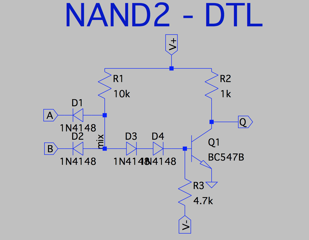
Back to simplicity : you may want to trade input transistors for diodes and save room and costs with DTL: Diode-Transistor Logic. Look at many projects around here, such as Pavel's, Alan's or Mat's. It's simple, it's slow, it's not too fussy about the power supply, it's all NANDs. You can even swap some parts for LEDs, such as Tim's #LCPU - A CPU in LED-Transistor-Logic (LTL) ! It's good to get started but your system won't easily exceed a few MHz of operating frequency.
Don't forget the speedup capacitor to short D3-D4.
You could use Schottky diodes like LL101 (1ns). There are faster Schottky diodes, and even 2 diodes in a three pin SMD package (that's going to be quite compact).
Add a Schottky clamp to the output transistor, it makes the gate faster, which also makes the gate output less sensitive to variations of the load.
Put a 56k resistor or such in parallel to the Schottky diode, or else your gate inputs might be getting a hysteresis which increases with frequency
Keep in mind that DTL piles up quite a bit of capacitance when wiring some gate inputs together.
In fact, as you want to go faster, you'll have gates that have more parts than ECL and you'll slowly drift into TTL territory. And you're still stuck to NANDs. But it gets you started...
If DTL is still too modern or fast for you, just fall back to plain old RTL: Resistor-Transistor Logic, like they did back in the 50s and 60s. But this is pretty close to DCTL (Direct-Coupled Transistor Logic, a sort of DTL with less fuss, as used by Cray in the CDC6600 in the mid-60s) and with some care, DCTL can get pretty fast even with old parts: about 5ns per gate can be reached. The parts count is reasonable but this time, you're stuck to only NORs.You must also have one version of each gate for each fanout, or allow the output pull-up resistor to be changed. It's not too fussy but you still have to care about the saturation.
While we're still on the Cray chapter, the next interesting family is ECL: at first intimidating, "non-saturating logic" has several qualities, among which speed is the most known. On top of that, the basic gate can do both NOR and OR, because the output is complementary, which helps a lot with complex boolean networks. The basic topology can be extended by "dotting" and cascading, easing the design of latches and arbitrary boolean gates. ECL can go faaast and our amateur tools are often the limits. Power is another major concern : each gate draws at least 2mA, regardless of the state (that's 10mW @5V). This simplifies filtering but heat management is a famous drawback. @Tim added a new twist to the story with #LED Coupled Logic (LCL), where gates that only need the inverting output can save several parts, with the substitution of a few diodes in series. It's alluring (fewer parts, still fast) but you end up back to "only NOR" domain, and with a probably similar speed as the above DCTL, you still consume more power (this must be tested and verified though). Willmore said this : As you seem to have discovered as well, RTL and DTL have a lot of drawbakcs and aren’t easier to use than ECL (and having the option of
every signal being differential gives free inversion). Anyway, ECL is worth a try, if only because it's one of the most "expressive" families. This flexibility provides more boolean functions per discrete part. The problem with ECL is line distribution and line termination, and getting this right would take some more years of experimentation, as well as some serious lab tools...
NMOS/PMOS was the first successful non-bipolar technology, it is easy to build with discrete parts, the Megaprocessor is a famous example. It's good for beginners but it suffers from the same "pull-up" issue as RTL/DTL/DCTL and even ECL: the speed is limited by the output resistor. Worse: the cheap discrete MOS parts have significant gate capacitance. Most implementations use NMOS because discrete PMOS is significantly more expensive, so no mix&match and funky topologies here. Conclusion: you're still stuck to NORs.
CMOS is the king on silicon today, but is hard to build out of discrete parts. Several attempts have been documented but no significant circuit has been implemented. This is because commercially-available MOSFETs have their "bulk" tied to their "source" and pass-logic is much harder. Even the BS170/2N7002 are designed for medium power switching, and their gate capacitance is significant. However "pure CMOS" is highly expressive, many topologies easily provide AND/OR/NOT combinations and are a primary aspect of ASIC design.
Note that if you are not concerned with raw speed, and you're willing to deal with saturation and weird levels, you can play with less advertised aspects of transistors to create some shortcuts and extend your "expressiveness":
Bipolar Junction Transistors can be seen as ANDN gates. This can be useful in certain cases and it is the basis for the classic 2-transistors XOR gate, but it requires "regeneration" (an output buffer, often inverting)
Pass logic is also possible : it's common for MOS, but a BJT can also act as a logic pass gate. It's ugly, but it can sometimes work...
However these "analog tricks" break the principle of a "logic family" where every member can be connected to the others.
. .
The conclusion of this exposé is simple:
Apart from ECL which offers some flexibility, most discrete logic families are restricted to NAND or NOR gates.
You have to adapt your logic design, architecture and physical parameters to the family you choose, and learn to break most boolean circuits into NORs or NANDs, it's a skill that is learned like a language.
This also means that if you can express your architecture as a collection of NOR gates, you are then free to implement it with several types of logic gates, which you can choose with more freedom. In fact, I found only recently that NOR is the more natural choice for many families than NAND:
NAND is the natural gate of TTL and DTL
NOR is natural for ECL, RTL, DCTL, NMOS...
You can twist and tweak the rules if you get access to complementary parts (as with IBM's "current steering logic" which was the precursor to ECL) but then the design would become too specialised and less portable.
Each is optimised for a specific purpose and things get nasty when they are mixed.
mix data and program memory, and you get a lot of security troubles.
mix data and special memory-mapped registers, and you kill your system that must recognise IO regions and addresses, as well as ordering and write-through/writeback/grouped/caching attributes
mix data ram and registers and it becomes ridiculously slow (TI tried this last with the TMS9900 and you see what happened)
... you get the idea.
...
Update 20240625:
That was a starting point. I now consider it "bad" to mix que control/return stack with the data space, and the latter is split in private and public areas.
 Yann Guidon / YGDES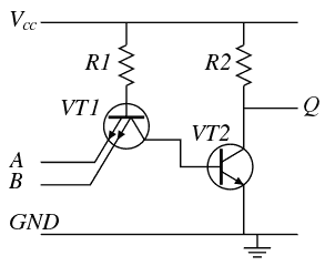
 You can even swap some parts for LEDs, such as Tim's
 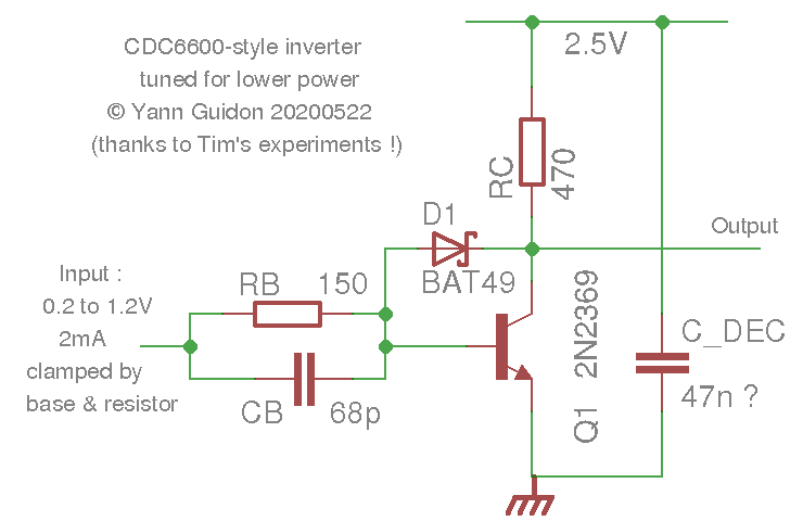 You must also have one version of each gate for each fanout, or allow the output pull-up resistor to be changed. It's not too fussy but you still have to care about the saturation.