Jithin
-
Calibrating the uC ADC for maximum accuracy
08/03/2015 at 20:38 • 0 commentsUPDATE(11-Aug)
First, the results of the calibration!
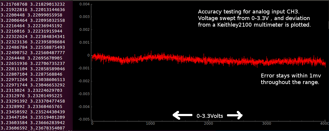
Random values are input to CH1, and CH3 of the vLabtool, and are simultaneously monitored via a KEITHLEY2100 DMM in order to highlight the accuracy, and noise levels of the different input channels. The DMM seems to add noise to the voltage source, and this is highlighted towards end of the video, wherein one can see that disconnecting the DMM improves the signal quality.
![]()
Sample test results for CH3. a 0-3.3V sweep was generated with a 12-bit DAC, and the errors were plotted
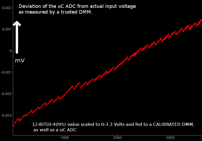
------------------------------------------------------------------------------------------------------------------------------------When it comes to digitizing analog levels, a number of factors prevent the output codes of the ADC from corresponding perfectly with the input voltage. Even if one somehow reduces noise levels to far below the resolution of the ADC, non-linearity issues as shown in the following image will persist. And these are inherent to ADCs.
![]()
For obtaining the data shown in the above picture, things were kept simple, and no input buffers/gain stages were used.
The output of a DAC was fed directly to an analog input, and the same voltage was also monitored using a calibrated 24-bit voltmeter.
Therefore, if the reference voltage of the ADC (3.3v) does not change, this pattern should be easily repeatable. In order to ensure that, the vLabtool uses a 3.3V voltage reference (REF196) which will stay consistent to within a few ppm over a wide temperature range. The Vref does however, have an initial offset up to 10mV which can be trusted to not drift more than the specified accuracy.
How does one calibrate the uC ADC?
A) The easiest way would be to record the deviations for each input code, and save them in a lookup table. Since the resolution of the ADC is only 12-bits, you'll have a lookup table with 4096 entries. If each entry is a byte, you'll need 4kB of storage.
* In the picture shown , the resolution appears to be much better than 12-bits at 0-3.3V (theoretical resolution = 3300./4096 mV) , and this is the result of oversampling .
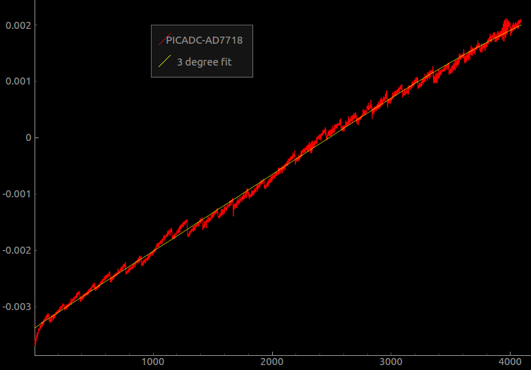
B) Another approach would be to simply fit the curve with a finite polynomial, and use the equation for calibration. However, the arbitrary non-linear staircase pattern has proven to be very hard to approximate to an equation.
Here's a polynomial fit of the above. A second order polynomial was generated using numpy.polyfit and numpy.poly1d.
![]()
What one could do , is store the fitting polynomial, as well as the deviations from the fitting polynomial.
And a two step calibration can then be applied to obtain a pretty accurate 12-bit ADC performance from your uC.
Will one have to store calibration tables for each analog input (most uC have multiple analog inputs)?
Not likely. Each input is usually routed to the same analog to digital convertor internally via a multiplexer (refer to the datasheet).
So in summary, only one table will have to be stored per ADC, and polynomial fitting functions will be required for each analog input in case you're using opamp buffers or other components which introduce predictable slopes and offsets.
What does this mean for the vLabtool?
The vLabtool has several analog inputs with various voltage ranges (+/-16V, +/-3.3V , 0-3V 0-9V ... ) , but after associated analog circuitry ( hopefully all will have only smooth variations from the actual ) , the signals end up at the same ADC. For two-channel, and four-channel capture routines, a total of four sample and hold capacitors are present, and these take a snapshot of the voltage which are then digitized one by one by the same ADC.
Therefore, the approach I have decided to follow, is to store the deviations for the ADC in a 4KB space in the flash memory, as well as polynomial coefficients for each of the various analog inputs.
Preliminary results -
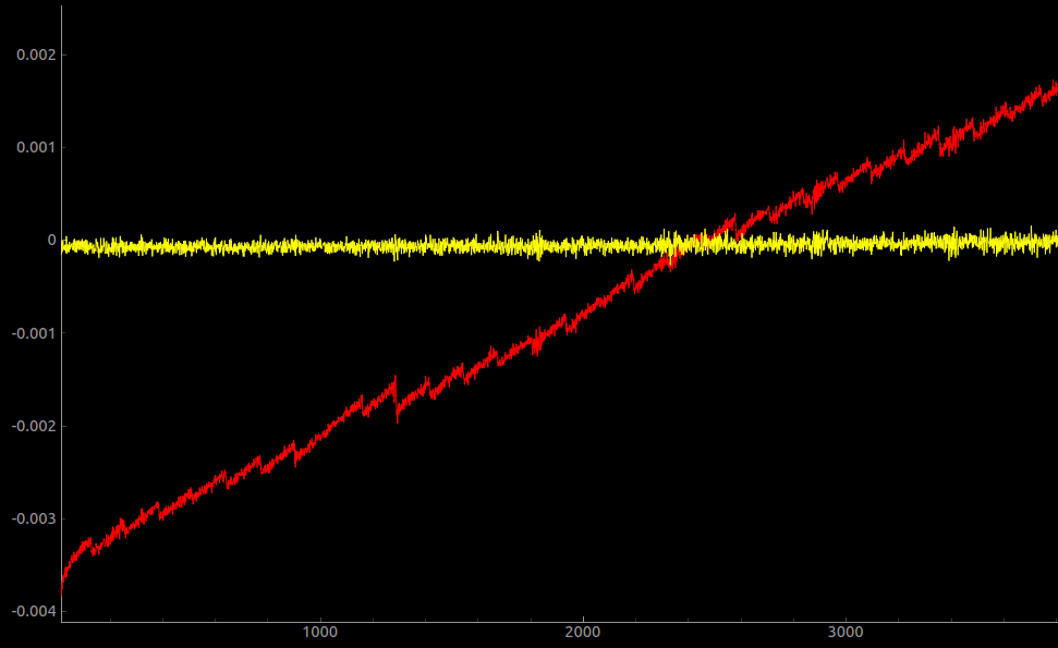
![]()
The Red trace represents the deviation of the ADC from the actual input voltage over a 0-3.3V range [ the non-linearities at the ends of the spectrum are not shown]
After the calibration table is applied, one ends up with the yellow trace whose maximum deviation from the actual value stays within 250 micro volts throughout the usable range of the ADC!
If the user requires better resolution and accuracy , they can always choose an add-on board that best fits their needs. The one used as a DMM for the above results was an AD7718 which was calibrated against a KEITHLEY 2100 DMM. The add-on PCB used highly-linear op-amps as buffers, and a REF196 voltage reference. The add-on board has been documented here, and the automated calibration process is here
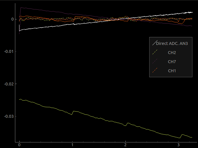
Calibrating all inputs together, and storing values to flash...
![]()
The white trace is data measured from an unbuffered, unaltered analog input , and represents the deviation from the actual value. The sawtooth nature of this curve is the non-linearity of the ADC itself, and will be subtracted from all subsequent readings from the other channels. After this correction, the slopes and offsets of each channel will be stored to flash along with the INL lookup table.
In the figure, the continuous lines represent errors of the uncalibrated inputs, and the dotted lines are generated by applying the two step calibration. Unipolar(0-3.3V) inputs are accurate to less than 200uV, and bipolar inputs (+/-16.5V) are accurate to less than 1 mV after calibration.
if you're wondering why the steps are much wider for CH2, and CH1 (green and orange traces ), it's because the steps are characteristic of the ADC, and these inputs can accept voltages between -16.5V and 16.5V . These voltages are then scaled and shifted into a 0-3.3V range, following which the actual digitization takes place. So a 0-3.3V range for CH1 / CH2 is actually something like 1.65V to 1.97V for a direct analog input like AN3(the white trace) . The step widths will match if you scale by a factor of ten.
UPDATE(11-aug)
Calibrated three units for the Best Product category yesterday, and managed to test the performance against a KEITHLEY2100 multimeter.![]()
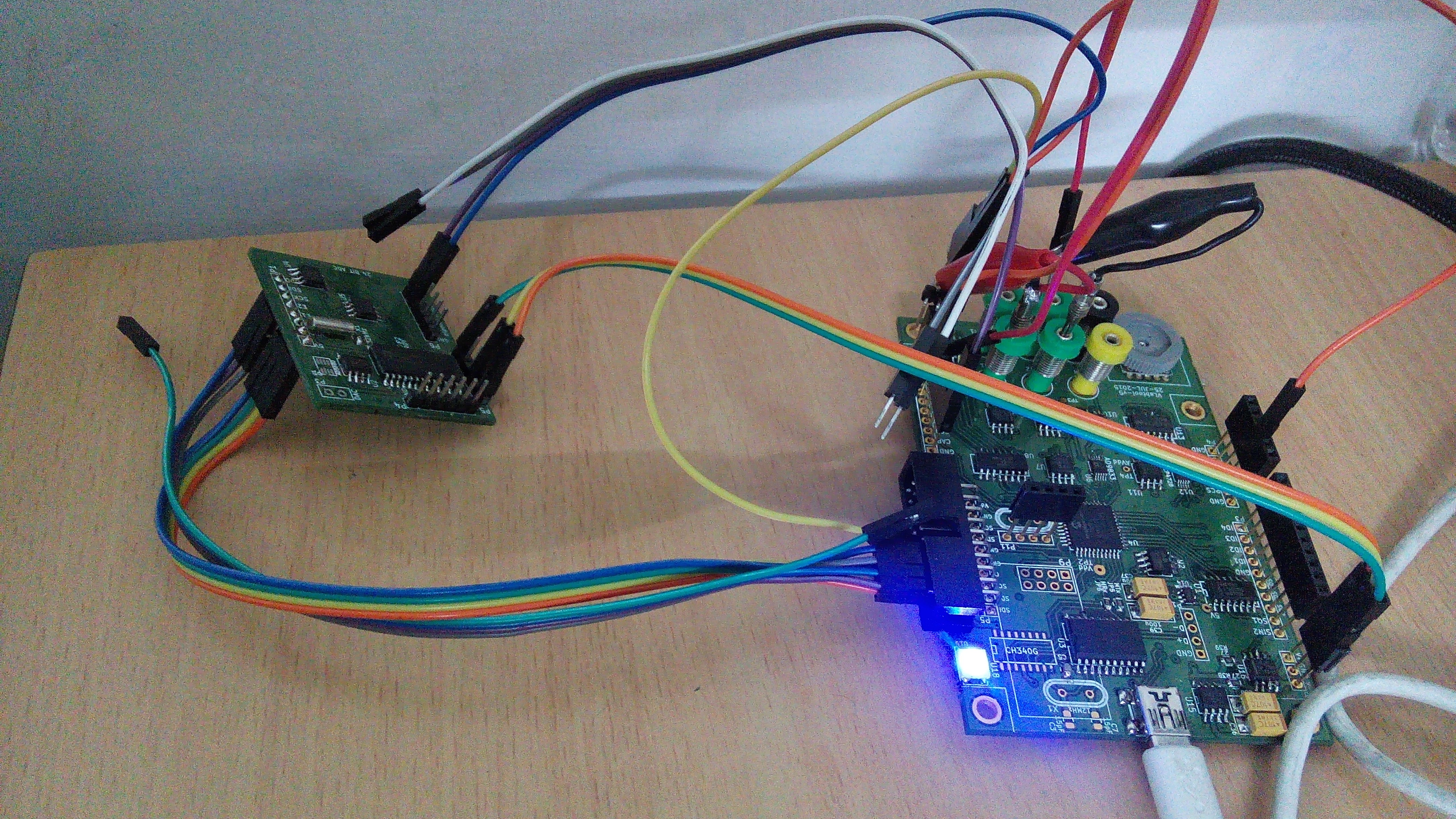
The calibration rig that was used. A custom PCB with an AD7718 24-bit ADC was first built and calibrated against a 6 digit DMM. It was then connected to the SPI portion of the expansion slot of the vLabtool, and used for the calibration process.
The process itself involved sweeping the output of a 0-3.3V DAC and feeding it to inputs CH1,CH2,CH3,CH4, AN3 and the AD7718.
AN3 is directly connected to the uC, and is used to obtain the INL of the ADC. The slopes and offsets of the other channels are calculated after subtracting the INL. The AD7718 serves as the 'actual' value readout.
The calibrated units were then tested against the Keithley2100 connected via USB, and interfaced using python-usbtmc. The test results and video are right at the top of this log -
Building Blocks: 15KHz standalone sine wave generator
08/01/2015 at 19:49 • 0 commentsIn an effort to keep costs low, the vLabtool only has one high resolution DDS sine wave generator incorporated onto the base board. However, certain electronics experiments(such as Amplitude modulation) require two waveforms.
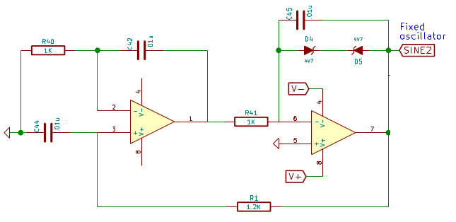
Therefore, a fixed frequency quadrature oscillator was added at the cost of an op-amp and a few passive components. The output waveform is bipolar, with a fixed amplitude.
![]()
This fairly common circuit generates a sine wave and a cosine at the same frequency. D4,D5 are 4v7 zener diodes.
-
Building Blocks: 28-bit sine/triangle wave generator
08/01/2015 at 12:01 • 0 commentsA waveform generator is a must for studying a variety of electronic phenomena such as resonant frequencies, filter characteristics, etc. , and the vLabtool includes a 28-bit DDS( 0.03 Hz resolution at 16MHz clock.) with manual amplitude control from +/-20mV to +/-4V.
The DDS(Direct Digital Synthesis) Approach to waveform generation involves a pre-programmed lookup table containing the amplitudes of the waveform to be generated. The processor then loops continuously through this table, and feeds each amplitude to a DAC, resulting in an analog waveform being generated at the output.
![]()
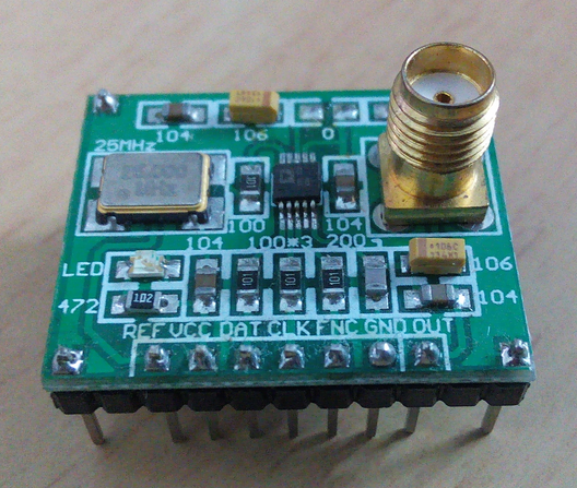
Initially, I ordered a couple these breakout boards for the AD9833 DDS. Once the communication protocols and usability were confirmed, it was added to the base board. The output of this breakout is 0.6v p2p (DC blocked with a capacitor).
Additional circuitry required to make a usable output.
- The amplitude of the AD9833 is fixed at 0V - 0.6V for the sine and triangular waves. This felt rather restrictive . Adding a level shifter, and manual gain control results in a bipolar output which can be adjusted from +/-10mV to +/-4V.
Frequency control
- Two 28-bit frequency registers are present on this IC. This is aimed at applications like Frequency Shift Keying. Once both frequencies have been loaded, one can quickly toggle between the two. The maximum clock frequency is 25MHz , and this allows generating waveforms from 0MHz up to 12.5MHz(If you're okay with 2 points per waveform). On the vLabtool, the DDS is driven with a 16MHz clock generated by the PIC24E . 16MHz,28-bit equals 0.03Hz resolution. Neat looking frequencies can be seen up to 2MHz. Beyond this, the scarcity of points will force using another analog filter.
- A 12-bit phase register is also present, and this can be used to set a fixed phase difference between two AD9833 ICs running off the same clock, and outputting the same frequency( or a harmonic ). The phase registers have been used on the Python Powered Scientific Instrumentation Tool since it has two AD9833s on the base board itself. Phase control won't be useful on the vLabtool unless an Add-on board with another AD9833 is used. Keeping this in mind, the 16MHz clock of the AD9833 is also routed to the 20-pin expansion slot.
![]()
This is the portion of the schematic that deals with the AD9833. The gain control slider is a 50K dial potentiometer.
Choosing an appropriate DC blocking capacitor is essential for achieving constant amplitude throughout the frequency range. I actually experienced this when I accidentally used 0.1uF instead of the 10uF. Since the vLabtool also has an oscilloscope, it was used to record the output for frequencies spanning the intended range. The output curves were fitted using Scipy, and the extracted amplitudes were plotted against the corresponding frequency.
![]()
Figure: ERRONEOUS frequency response curve of the DDS resulting from a misplaced capacitor! . Ignore the blue trace, it's not relevant here.
Replacing the 0.1u with the right value(10uF) gave an extremely flat amplitude response at 4V starting from 5Hz.
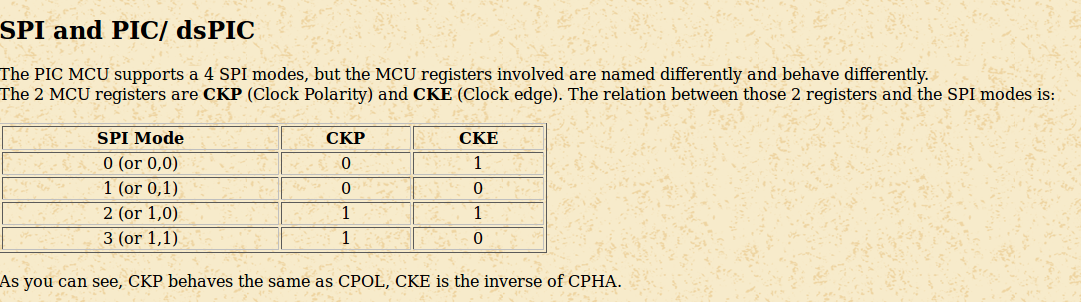
The SPI input of the AD9833 is very picky when it comes to modes. Both CKE, and CKP must be set to 1. Accidentally pushing values with wrong mode settings causes the IC to not respond until a hard reset. All this has been taken care of in the firmware. In case you're not familiar with CKE, CKP terminology, here's a map (taken from here).
![]()
-
Artist's impression of finished product
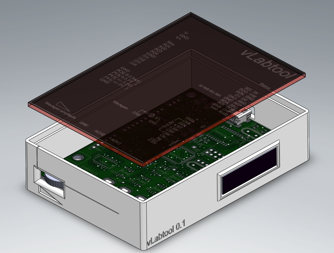
08/01/2015 at 10:56 • 3 commentsSo far I've designed a 3D enclosure using SolidWorks. The bottom will be 3D printed for now, and any errors can be rectified before going for an injection mould. The top plate will be laser cut and engraved in translucent acrylic, and added .
![]()
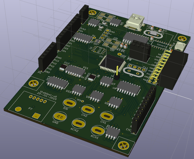
Figure:3D rendering of the PCB designed with KiCAD.
A SolidWorks render will have to do as an 'artist's' impression
Here is an exploded view of the designed case. It would've been great to be able to use the 3D generated objects from KiCAD, but it seemed impossible to use them in a SolidWORKS assembly. Instead, I took a screenshot of the PCB, and overlaid it on a 65x95 part with similar thickness. The overlay allows me to roughly determine the position of objects without referring to KiCAD, or measuring manually. AUX jack shown was a quick sketch-extrude-cut job.
![]()
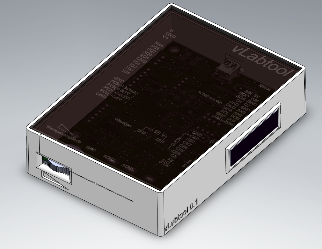
I really wish the kicad 3D output had played nice with SolidWorks. Now you'll have to picture the fully populated circuit board yourself. And you've already seen the 3D printed box on the main page anyway.
![]()
Here's the Splash screen for the App framework. The PNG is transparent.
Was created with GIMP.![]()
-
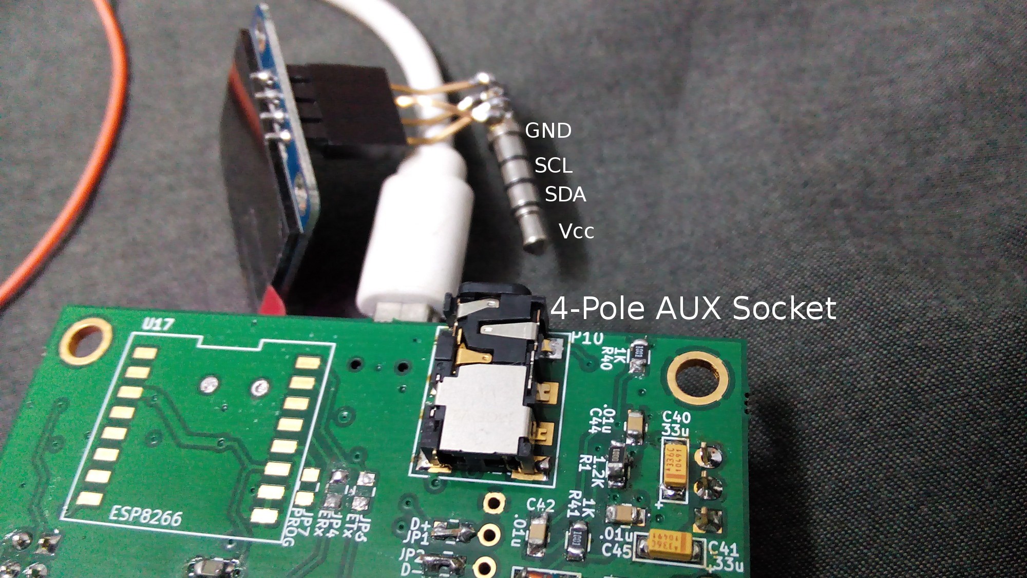
4-Pole 3.5mm socket for sensors that speak I2C
07/26/2015 at 21:19 • 0 comments![]()
Having to Plug in numerous wires in a particular order each time is an unnecessary hassle as well as a risk. In case of sensors that speak I2C , four connections (Vcc,GND,SCL,SDA) need to be made. The Clock and Data lines can e shared over multiple devices.
Using a 4-pole socket has numerous advantages
- It eliminates the need to make multiple connections for one device, and also rules out the possibility of errors and mishaps.
- Since these cables are already a mass market product, good quality ones can be procured at affordable rates.
- 4-pole splitters can be designed in order to Plug and play multiple sensors [However, The wireless nodes may also be considered here if one can live with a 3mS round trip delay].
![]()
At this point, I2C lines are available on the 20-pin expansion slot, a 4-pin berg pin on the center of the top panel, and over the 4-pole 3.5mm socket
-
Controlling Daisy Chained Addressable LEDs
07/26/2015 at 11:09 • 0 commentsOne of the pins from the expansion slot carries signals to drive daisy chained WS2812B RGB LEDs (Certain Neopixels from Adafruit use this model ). Each RGB LED supports 24-bit color(16-million shades) and they can be addressed using a simple python command that accepts a 2D array containing color info for each LED.
A demo app was written using the ColorPicker button that's part of the PyQtGraph toolkit that's used extensively with the vLabtool. The button launches a QColorPicker Widget for each LED in the chain, and the colors are set using
#Set colors red, green, and cyan on LEDs 1,2,3 I.WS2812B( [ [255,0,0],[0,255,0],[0,255,255] ] ) -
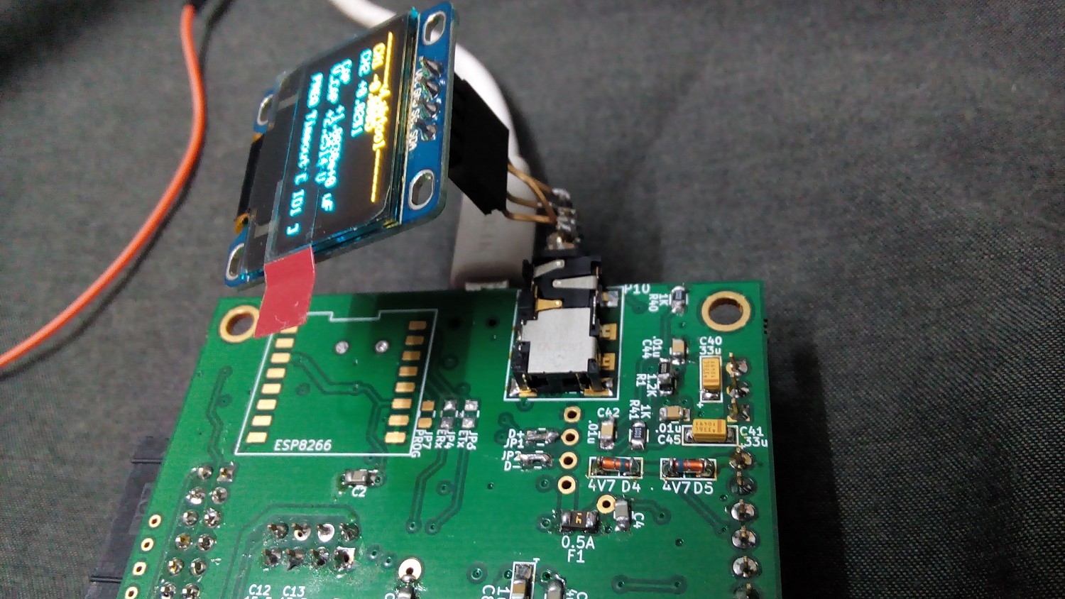
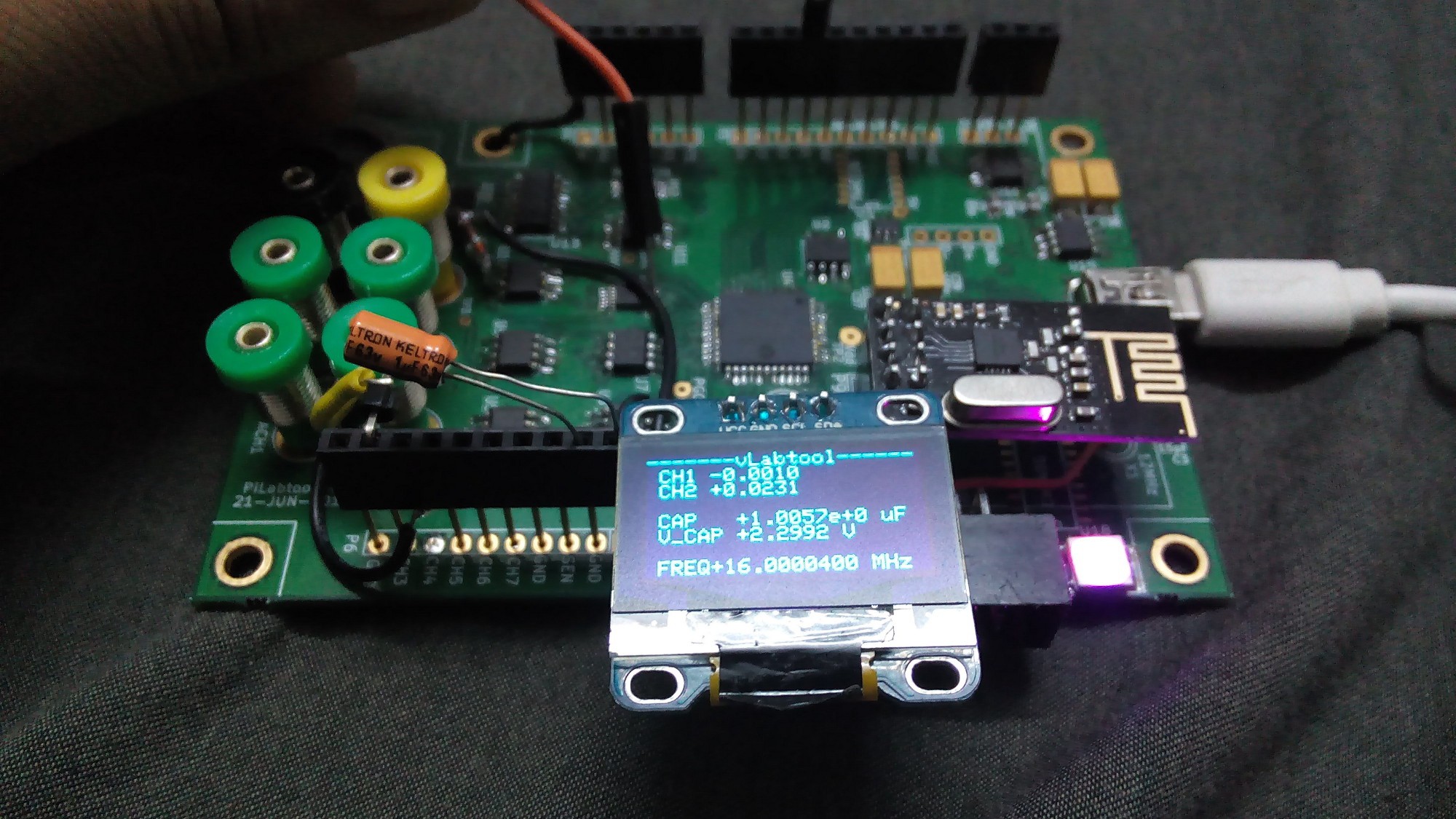
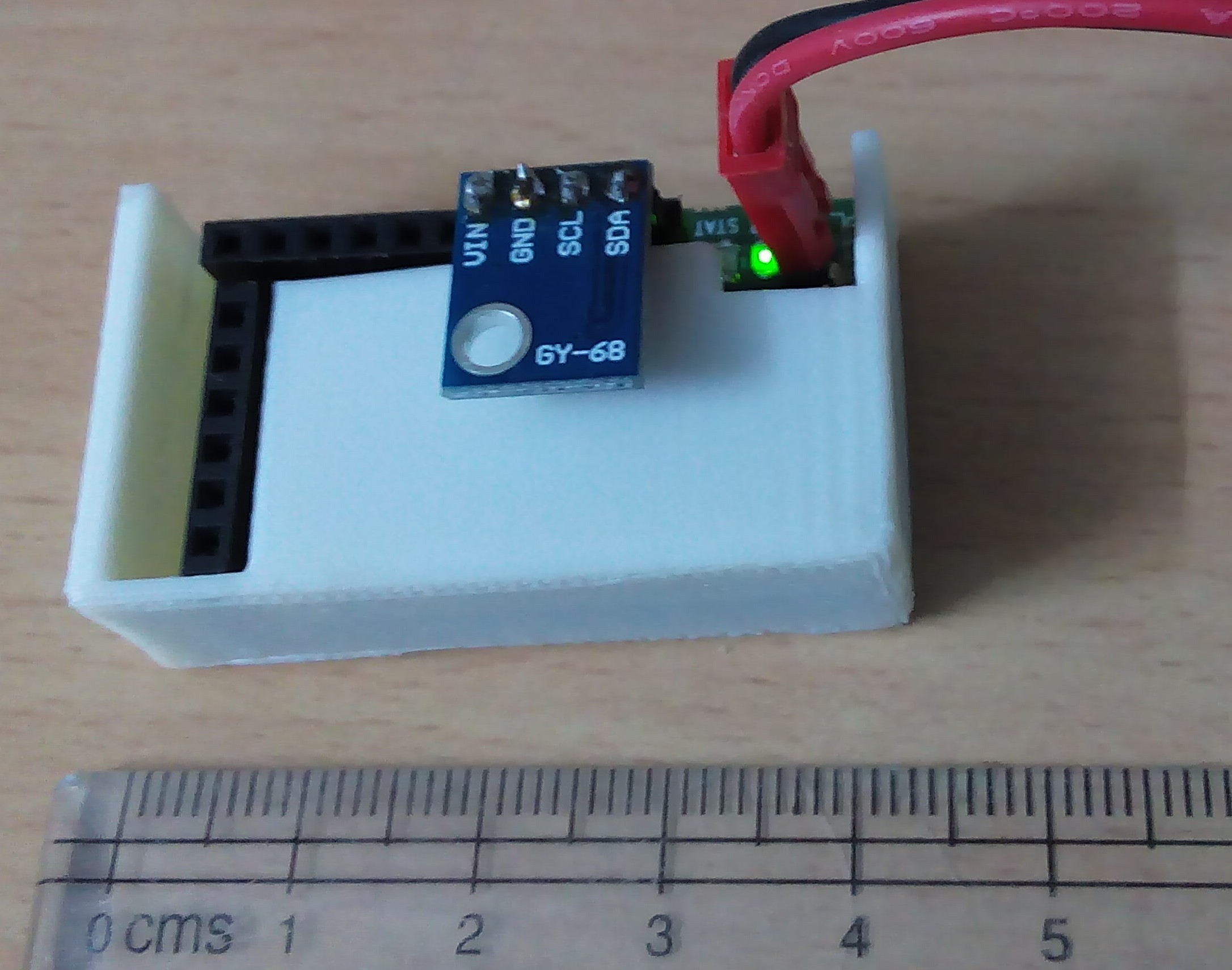
Standalone Mode using a 128x64 OLED
07/26/2015 at 10:12 • 0 commentsIn keeping with the modular design that enables costs to be kept to a minimum without compromising on capabilities, a standalone mode of operation is being added to the firmware.
This will display a few basic measurements such as capacitances, voltages, frequencies etc on an ssd1306(128x64) OLED if it is detected on the I2C port when the device powers up. The device can be run off of batteries or other power sources.
Once it receives data from the PC, it will automatically exit the standalone mode and a remote/hard reset will be required to restore it.
![]()
The Picture Above shows the present state of development of the standalone mode.
Polynomial based calibrations are not applied , and instead nominal values for references are used.
CH1,CH2 are floating, and are displaying a few fluctuating readings. The capacitance of 1uF capacitor is calculated using constant voltage charging mode, and the potential developed across it at the end of the charge cycle is also shown. If a diode is plugged in instead of a capacitor, this voltage approximately represents the barrier potential.The frequency of the clock fed to the AD9833 DDS is also measured. However, since the clock source is correlated to the 12MHz TCXO that is also used as a reference for the frequency counter by means of a PLL, the readout may have an error of up to 2.5ppm as stated in the datasheet of the FOX924b 12MHz TCXO.
The display projecting out awkwardly isn't a good solution, so a centrally placed four pin I2C header has been added to the next layout sent for fabrication. -
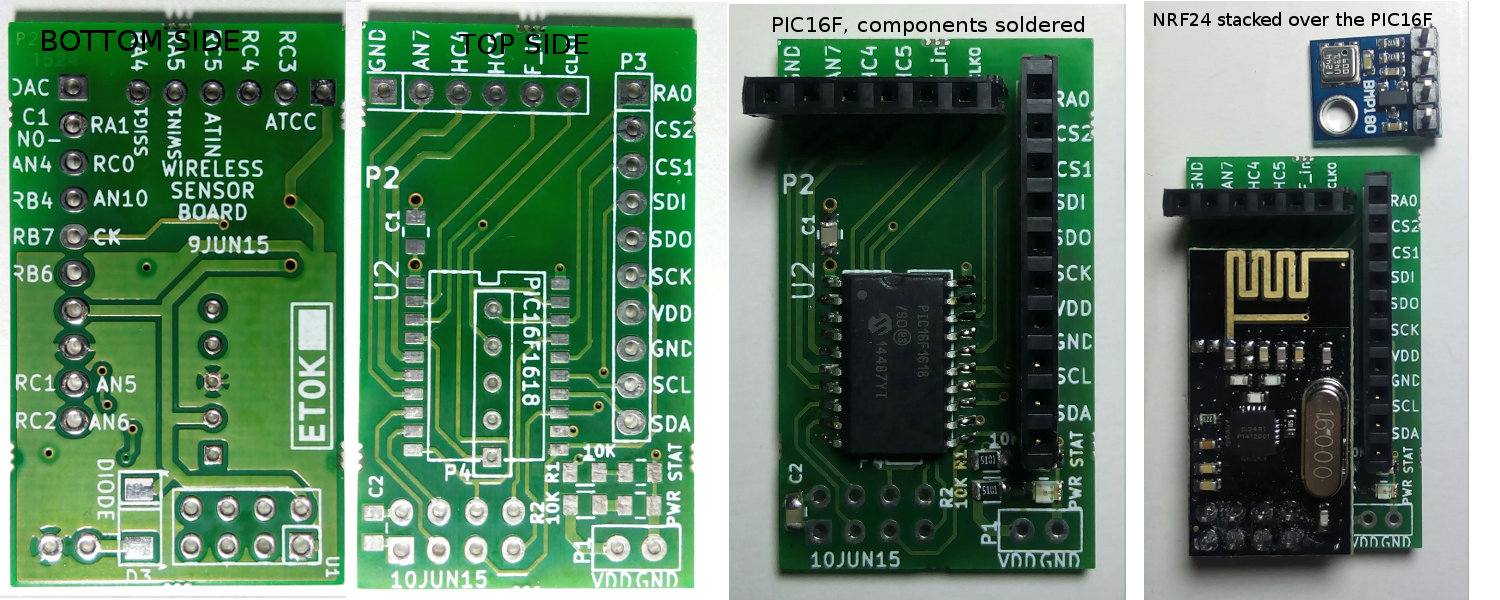
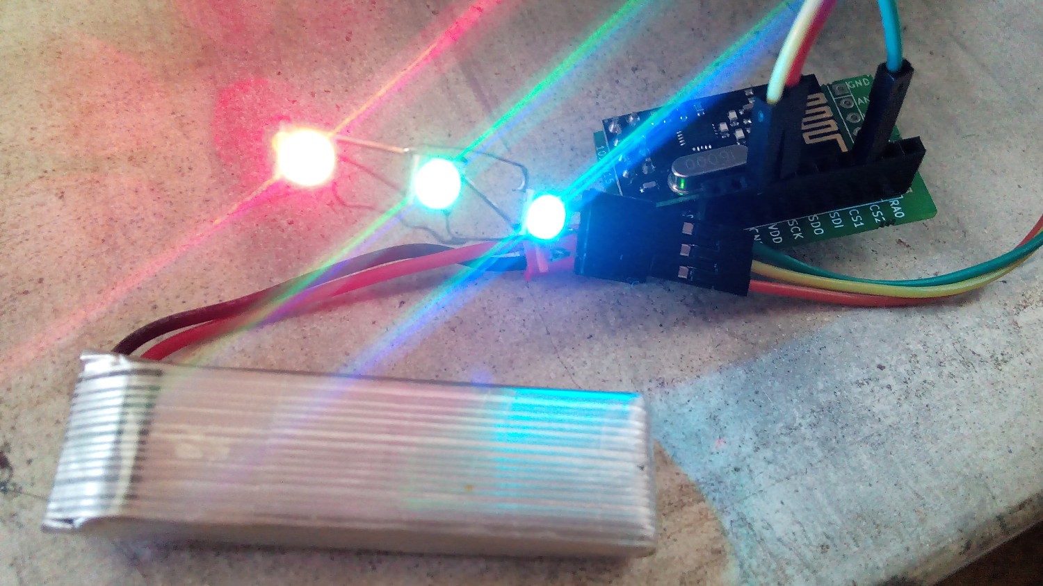
NRF24L01+ based wireless nodes
06/29/2015 at 13:51 • 0 commentsThe vLabtool has a dedicated wireless transceiver on-board. Slave nodes consist of a PIC16F+NRF24L01+ with unique 3-byte addresses.
Theoretically, up to 2**24 nodes can be controlled from one vLabtool.
KiCAD Design files on Github.
Each Node is currently capable of the following:- Speak to an I2C device that is supported on the Python side of things ( Not complicated at all. This is simply a python class contained in the SENSORS submodule of the vLabtool package. Users can easily add their own )
- Scan for I2C devices.
- Read voltages on various analog inputs.- Control daisy chain of WS2812B addressable LEDs
- R/W to NRF24 registers
- Broadcast Mode: In addition to their unique receive addresses, all the nodes have a common receive pipe. Any packets sent to this address will be picked up by all the nodes simultaneously, and will not be acknowledged to prevent collisions. Big things have been planned with this functionality.
- 8 - bit DAC
- Digital output
![]()
![]()
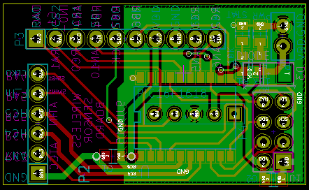
The layout is minimal
![]()
Basic functions have been broken out into berg strips. Digital functions include SPI/I2C/EUSART ports. Several inputs can also serve as analog inputs connected to a 10-bit ADC. There is also an 8MHz clock generator, and an 8-bit DAC. For now I've marked the default functions of the pins on the PCB wherever applicable.
Should've thought of adding a boost regulator for battery powered applications.I'll make the next prototype using the PIC24E since it has separate I2C and SPI ports in addition to a wide array of other peripherals.
In addition to the basic functions, the PIC16F has several interesting peripherals such as angular timers(http://ww1.microchip.com/downloads/en/DeviceDoc/30010090A.pdf), hardware PID etc. These may soon come in handy for implementing science demos/experiments.
![]()
3-D printed case for basic protection.
-
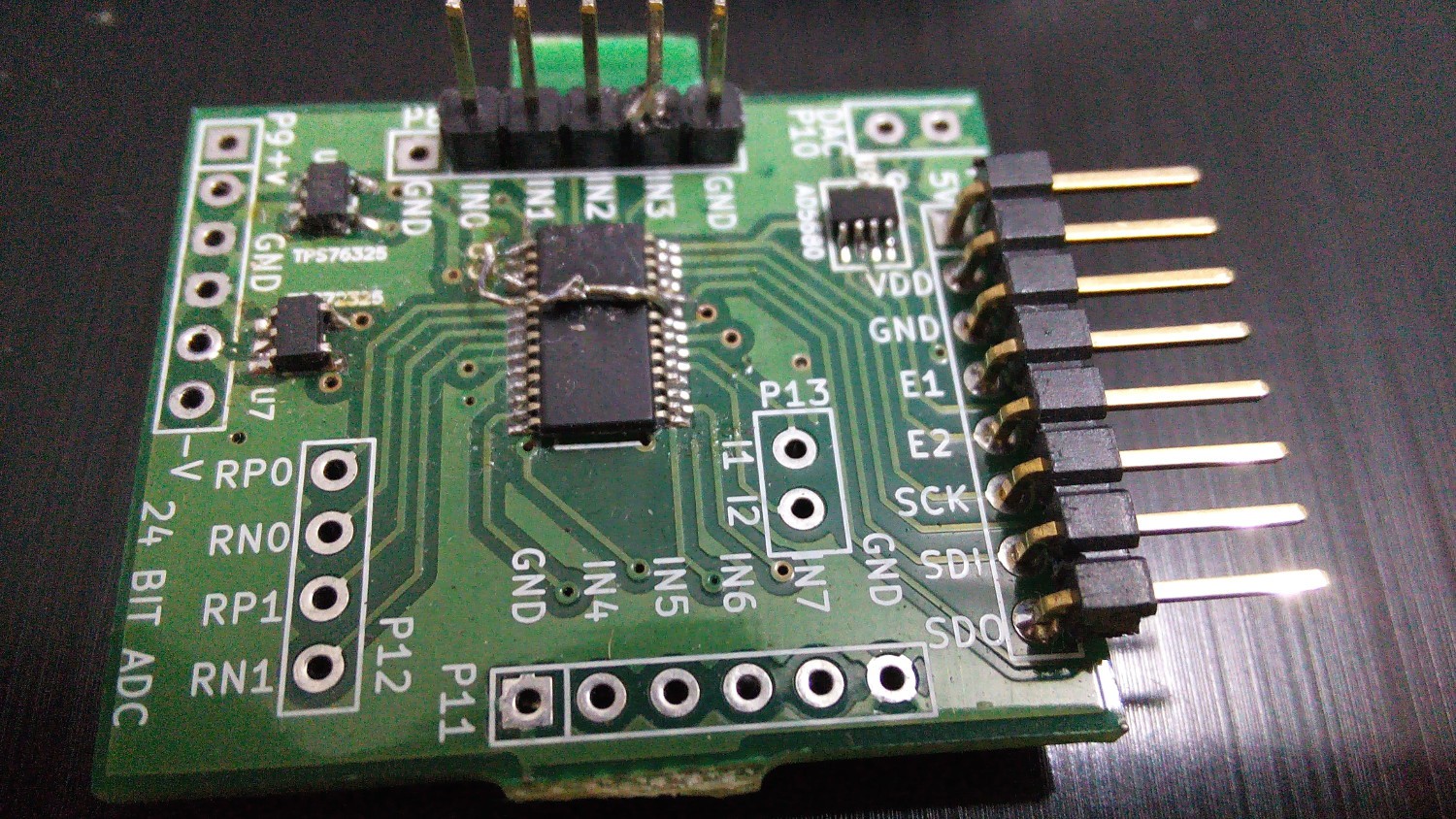
Add-on board: 24-bit ADC, 18-bit DAC
06/28/2015 at 22:21 • 0 comments![]()
This was a breakout board built for trying out the ADS1248 24-bit ADC as well as the AD5680 18-bit DAC. The final version should include opto-isolation and a standard 20-pin header compatible directly with the expansion slot on the base board among other things.
+2.5, -2.5 volt regulators ( TPS76325, TPS72325 ) are present in order to provide reference voltages for the ADC.
In order to get data from the ADC using a simple python script, the SPI as well as the power supply connections must be made to the base board. Following which, carefully perusing the datasheet will let us construct Python functions such as
def writeRegister(self,regname,bytes):
	I.SPI.start(csn) #lowers Chip select
	reply=[]
	reply.append(I.SPI.send8(0x40|regname))
	if len(bytes):
		reply.append(I.SPI.send8(len(bytes)-1))
		for a in bytes:
			reply.append(I.SPI.send8(a))
	I.SPI.stop(csn) #raise chip select
	return reply
This board has not been fully tested , and I expect the built in excitation current sources will come in very handy for measuring voltage drops across resistive loads such as RTDs and load cells.
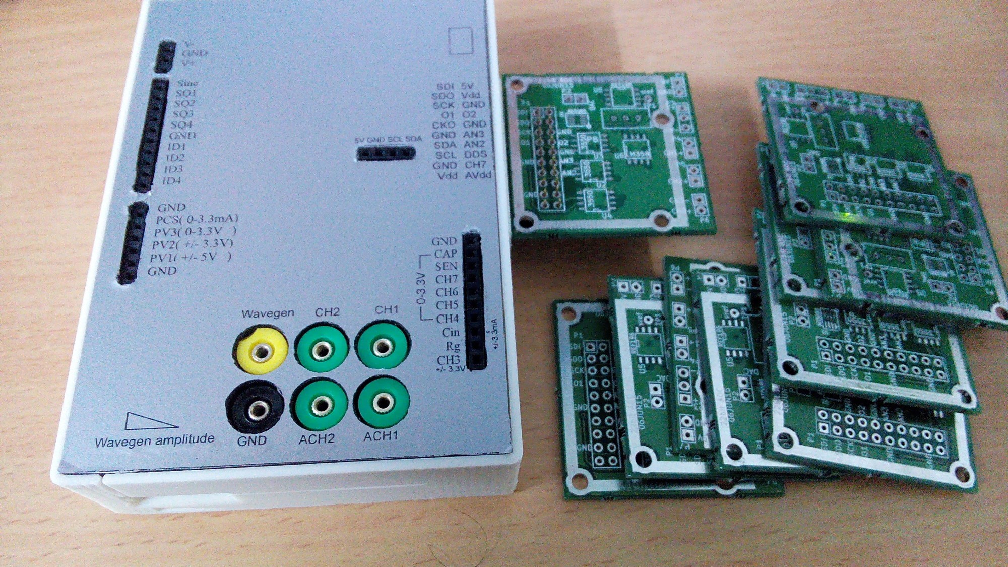
A 22-BIT ADC board with three MCP3550 on board. Two of these have level shifted inputs, while the third is a direct in.
A ref196 has been placed as the voltage reference IC.![]()
A Versatile Labtool
A cost effective, multi-pronged data acquisition tool to turn your computer into a workbench for science and electronics experiments.