Close
0%
0%

PCB /SMT MAKER LAB @ Home

This project outlines how to do advanced PCB making at home with proper tooling. Tooling includes a laminator and hobby laser.

Similar projects worth following
There are many approaches to making PCBs, but as we move toward more surface mount prototyping and more compact boards with small details our processes need to be refined and quality control upgraded. EM Compliance and ROHS standards are also driving how we produce and document our prototypes for down stream cost effective manufacturing. IoT designs may require good RF/VHF/UHF PCB characteristics as well. SMT reduces parasitic LCR components.

This project = optimizations for PCB making & cutting @ Home
I am an I.Eng with CISCO and M.I.T. certifications in I.C.T. & Electronics and I have been a maker a very long time now..

Optional: http://hackaday.com/2016/09/21/creating-a-pcb-in-everyth
SMD solder tut.:https://www.youtube.com/watch?v=hoLf8gvvXXU&feature=youtu.be

This approach to PCB making continues to employ toner transfer methods. The steps are as follows:

CAD DESIGN tips.

1) Design your PCB layout and add text 'silk screen' notations in the copper layer next to components if possible. I have found the EAGLE CAD vector font with 12% weight at a minimum size of .04" to .05" works well with this process. While you can add an extra toner transfer & a white foiling pass (post etching) for 'genuine' silk screening, I find it not warranted unless the PCB is single sided and you want to annotate the non copper clad side.

2) When pouring copper fills, ensure an isolation of 16 mil or more to achieve reliable toner transfer & foil transfer. 12 mil is possible but you will have to inspect and touch up with an Xacto knife for any bridging before etching.

3) Double sided boards need vias usually, I suggest upsizing the square pad to 0.031" diameter holes and .056" pad size for easy via location & assembly later. No more missed vias when soldering!

4) Locating machine screw mounting holes (6-32) requires a 0.125" drill and I suggest you add a .023" auto diameter round pad at the drill centre to mark the drill point in copper. I often use these at the PCB corners to help register/align both layers of toner transfer.

5) Always mark Pin 1 of any IC's with an asterisk in copper. Also always mark the anode of any diodes and capacitors with a '+' in copper. I also mark common SOT-23-3 transistors with a P or a N for PNP or NPN. This makes assembly much simpler as well as debugging. Note that the SPARKFUN lib has these SOT23-3 pad profiles made so that you can rout a 12 mil trace underneath an SOT23-3 transistor! That is quite helpful at times! I generally stay with 0805 SMT parts so I can rout a 12 mil trace underneath them as well. 12 mil traces can rout between 0.1" pitch thru hole parts such as IC's or headers as well.

6) Test points....most commonly I use a 2 pin, 0.1" pitch male header pad as a test point. This allows me to solder in a bare wire looped thru the PCB to make a loop on one or BOTH sides, if required, to 'hook' a 'scope probe or use DMM alligator clip.The wire loop is usually stiff wire from leaded resistor, capacitor or LED trimmings.

7) High current fills/traces: Augment high current, thick traces or fills with solder braid ...the used braid cuttings work fine, so I keep them on hand. This approach can also reduce the inductance of a trace such as a GATE drive for an FET to reduce 'ringing' or EMI issues.

8) As a manufacturing tip: I modified the standard 3 pin thru hole potentiometer pinout into a 4 hole version. The wiper then can use either of 2 holes . This permits substituting different potentiometers with different pinouts and takes advantage of manufacturer 'sales' or price breaks as often happens @ NEWARK. In the pics in this project you can find such pinouts in use. Note the 4 pin thru hole POT pinout with the connected centre holes just right of the LM317 pinout ; 1/4 width from the top right corner of this pic.-------------------------------------v
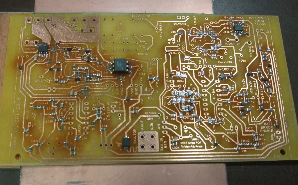
9) For double sided boards I always try to have a large ground plane fill/pour to mitigate ground resistance, ground inductance, and simply using vias to access a ground point. If you can't have a ground plane, use thick .024" or larger ground traces and star grounds if you have mixed mode analog/digital signals and switching currents to drive relays and such like. If you note the double looped 12 mil trace next to the large SMA SMT diode at the bottom of the image, that creates a free on board fusible link for any high current shorts in addition to on board PTC thermistor protection.

PCB electromagnetic compliance and electrical noise issues are outside the scope of this project but are related so here is a recent link that can assist. http://www.allaboutcircuits.com/technical-articles/clean-power-for-every-ic-part-1-understanding-bypass-capacitors/

See the Build instructions below the pics = making PCBs.

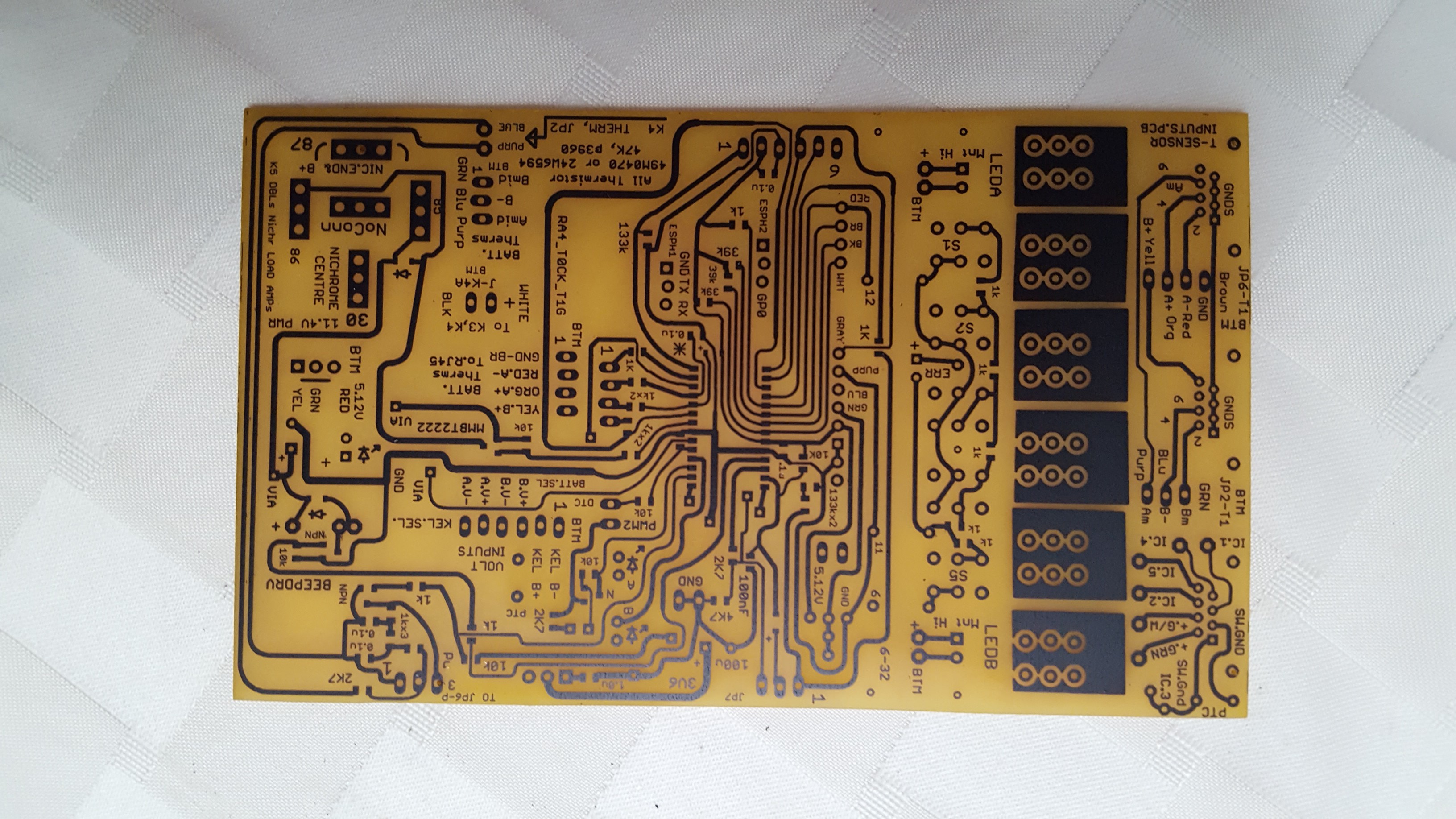
1-Toner transfer print.jpg

From generic toner cartidge HP1102W printer, 346°F transfer temp - 10z copper , double sided - 1.6mm FR1 PCB.

JPEG Image - 1.38 MB - 02/29/2016 at 05:13

Preview

2- Punch Registration to copper.jpg

Using a Krazy glue cap 'punch'

JPEG Image - 1.70 MB - 02/29/2016 at 05:13

Preview

2a-Registration_holes_drilled.jpg

Used the Proxxon Press for this - 0.8mm bit.

JPEG Image - 940.44 kB - 02/29/2016 at 05:15

Preview

2b-Copper-post220grit.jpg

Nice surface finish to grip toner.

JPEG Image - 1008.13 kB - 02/29/2016 at 05:14

Preview

2c-Iso-copper cleanup.jpg

Isopropyl alcohol wipes (70 to 99%) with a good paper towel is fine.

JPEG Image - 1.06 MB - 02/29/2016 at 05:14

Preview

View all 23 files

  • 1 × FR1 copper clad boards, double or single sided. FR4 for RF work, but can't be laser cut. Phenolic PCBS suitable for scoring and snapping or possibly laser cutting.
  • 1 × Craft foil used instead of Green TRF PCB making foil as a cheaper more available material with more colors. Search 'Heat Toner Foil Laser' on Ebay.
  • 1 × Dremel tool & press with carbide tipped drill bits-assorted sizes 0.5mm- 3 mm Thru hole components and machine screw holes.
  • 1 × Optional 6-32 or 4-40 Tap for machine screw holes in PCBs.
  • 1 × Toner Transfer paper- the Yellow stuff. Search 'Toner Transfer paper' on Ebay ...the yellow stuff!

View all 13 components

  • Double Sided using fresh HP toner @ 360F

    mosaicmerc10/27/2017 at 03:10 0 comments

    Did a test with a bit more heat with a fresh OEM HP toner cart for the 1102W printer.

    Very solid transfer and etch, no pin holing in the fills , did not use the extra foiling step. 5.5" x 3.25"PCB with SOIC part (28 pin) in centre and 0805 SMT parts.

    Also on ALIEXPRESS search for M0.9*2.5 Copper Hollow Rivet , to make  handling vias simple.

  • PCB slicing dust vacuum

    mosaicmerc04/12/2016 at 17:33 2 comments

    Well, PCB dust is an issue with the diamond cutting blade on the mini table saw . But it is so good at shaping and trimming PCBs that I upgraded the operation with a mini vacuum. An

    ArmorAll AA255 ...from Amazon, $39 for 2.5Gallon capacity.

    Now the mini saw sits in it's close fitting original box with a round hole in the side of the box for the flex vacuum hose to snug in. Works a treat, the dust is pulled in via the negative pressure in the box. The vacuum is also very good at cleaning up the swarf from the Dremel or Proxxon drill cuttings & grindings. It has serious suction, that includes metal cuttings!

  • PROXXON drill press upgrade

    mosaicmerc02/27/2016 at 19:51 0 comments

    Well I caved and purchased a mid tier Proxxon rotary tool and matching drill press and mini vise. I already had acquired a Proxxon KT 70 compound X-Y table before which works with the press as well.

    This tool is far more stable, with minimal run out compared to the Dremel 395 and 'plastic' press arrangement I had used to date. Plus it can do 20K RPM and has an independent speed control and on/off switch , which is better than the Dremel's unified control. I don't expect much broken carbide bits now.

    I modded the minivise to lock onto the press slide bar for precision work on small parts. 1, 6-32 x 1.5" screw was required.

    As with the Dremel I installed a 'back light' for illuminating etched PCB through holes. Basically a Jumbo super bright white LED running off an old Nokia 5V charger & a 220 ohm series dropping resistor.

    Note the pics in the upload area.

  • PCB slicing

    mosaicmerc01/20/2016 at 09:07 0 comments

    Well, my days of scribing and snapping PCBs are now over. Was a bit inaccurate and FR1 boards have a nasty chance of splitting.

    With this 4" table saw (portable desktop) unit:

    http://www.amazon.com/gp/product/B00AEZ70AO?psc=1&redirect=true&ref_=oh_aui_detailpage_o00_s00

    I can get precision, repeatable cuts at the cost of about 1/16" of PCB 'loss' when using the diamond blade as supplied. The cut is smooth and precise.

    Cutting with the toothed 'wood' blade also works but isn't as clean, causes copper swarf and about 3/32" of PCB is 'lost'.

    Highly recommend it! Blade swap in about 2 minutes with a pair of spanners or sliding wrenches.

    I cut the box it came in down to about 3" tall to place the whole unit inside and 'contain' all the 'dust' & 'dross' from the cuts....barely any back splash of dust that way.. I plan to make a custom variable 'fence' with my laser cutter. But a couple of small G clamps and a bit of 1/4" alum. channel is good for a quick adjustable fence at any time.

    Now I can make custom fit RF cavity filters using PCB material....how's that for a hack?

  • Full Spectrum 40 W 5th gen' hack' fix

    mosaicmerc12/03/2015 at 17:00 0 comments

    For those of you using this laser, you'd note that the you tube alignment videos for the optics/ mirrors don't emphasize that centering the beam in the lens as important.

    Well in vector cutting, it is important as noted here:

    http://www.buildlog.net/blog/2013/05/why-are-my-laser-cut-edges-not-straight/

    Although I had a perfect mirror alignment of the beam I still had this angled vector cutting problem....as the beam wasn't quite centered.

    I had to

    1) Adjust the nut and screw axle arrangement on the top roller pair to 'push' the z-axis top towards the front of the laser machine. this straightened up the sloped cutting parallel to the gantry.

    2) Drill a NEW pair of 1/8" holes for the laser lens assy to attach to the Z-axis vertical adjustment, shifting the lens assy to the left by 1/4" relative to the mirror above it. This located the laser beam in the centre of the lens.

    3) Drill and tap a pair of holes on the mirror above the lens to provide a 4 point mounting instead of a 3 point mounting for better mirror adjustment control. This proved to be not essential with the other mods in place.

    4) Loosen the 3 silver hex screws holding the mirror block (above the lens) to the roller transport mechanism and 'twist' the whole z axis (incl mirror & lens) about 2 degrees clockwise, then retighten the 3 screws onto the roller transport. These screws are located under the top rollers facing the laser tube. The clockwise twist works if the slopes of the cuts perpendicular to the gantry go from left to right. Twist the other way if your slopes are right to left.

    Items 2,3,4 straightened up the cuts perpendicular to the gantry.

    The end result is near square cuts thru 1/4" thick acrylic on all 4 sides and better beam penetration for the same power setting.

    They called it a "hobby" laser for a good reason it seems. You can improve it's precision & results with a bit of effort.

  • Thinking 3D additive PCB thoughts

    mosaicmerc10/05/2015 at 01:07 0 comments

    Having automated the doublesided PCB making, I find myself having to interconnect several boards using wire to board components and headers for more complex systems.

    Using the same tools to make the double sided board with more leverage on the 40W laser cutter i believe I can design doublesided boards in layered stacks. Building multilayered prototypes in an additive fashion.

    Now arduino type stackable modules come to mind, but for true high density systems I am looking at 1/32" thick FR1 PCBs or even flex PCBs which are etched in a manner to permit the 40W laser to cut the base material as required.

    Then sidestepping the 0.1" pitch headers, the boards are designed to mate together so that components on the bottom of one do not align with the components on the sandwiching boards. By etching properly and then laser cutting notches for components, it's possible for the boards to lay flat on each other with no spacing!. Using the same stencil cutting technique we can have insulating 'separators' between these sandwiched smt boards. Vias can be soldered in stages as the boards are layered, even blind vias are possible.

    Now this approach can potentially give a higher component density than regular multilayered boards as components can actually be 'embedded' inside a board sandwiched by multiple layers with other components stacked above embedded components in it once the intervening board layers offset the embedded component's height.

    Consider a sandwich of 4 layers of 1/32" PCBs, then SMT components on the inner side of layer 1 can well be buried completely by layer 4, permitting more components on layer 4 to occupy the same location displaced vertically. Again, insulating laser cut transparencies provide inter-layer isolation as required. By using layer separator insulating material such as acetate transparencies, mylar or kapton sheets (laser cut with required slots/holes) it may be possible to place solder paste dots on different copper layers to create bond points between successive layers to be reflowed after the layer stacking is complete!

    The out come of all of this could be a device perhaps 1/2" thick with up to 12 layers of double sided copperclad 1/32" material plus separators and several layers of stacked embedded components. All DIY @ Home, using the techniques described and the on hand tooling!

    Faraday cage effects, reduced EMI minimal board inductance, reduced signal latency for high speed digital processing and minimal form factors are all benefits. This brings electronic micro manufacturing a bit closer to home with micro prototyping capabilities!

View all 6 project logs

  • 1
    Step 1

    Fabricating Single & Double Sided SMT PCBS.

    1) Stick the Toner transfer paper (TTF) onto a sheet of regular paper at the top edge for easy printer feed & crinkle free printing. I use painter's/masking tape for the job.

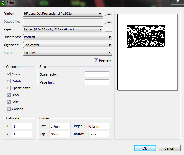
    When printing from EAGLECAD add a 40mm top offset to accommodate the painter's tape offset and print 1:1 scale, black, solid with top layer mirrored, pads, vias and dimensions active.

  • 2
    Step 2

    2) Remove the print and inspect it, if you hold it up to a back light you will probably see porosity in the copper pours or thick traces. Do not touch the printed surface or you can flake the toner. Cut out the print leaving about a (5mm) border around the perimeter to permit securing onto the copper clad board. Border cut does not need to be precise or perfectly straight.

    If you're doing a double sided board, Change the EagleCAD top layer setting to bottom layer (blue) and disable the mirror option in the print pop up. Print on fresh TTF for the bottom layer.

  • 3
    Step 3

    Go to step 4 for single sided boards.

    For double sided boards with thru hole parts: Place a TTF print face up on the board and align to take strips of painter's tape along the 5mm border. Secure with bits of tape on the sides. Now use a large safety pin or the pin cap from a Krazy Glue tube, carefully press a pinpoint punch mark in the centre of any thru hole pads near the corners of the layout so the copper clad is marked. I usually add custom pad/vias just for this purpose, perimeter machine screw locations are good as well. Once you have 3 or 4 corners marked, carefully remove the TTF print and use a regular 'bobby' pin to pass thru each punched hole in the TTF. Now take the other TTF layer print and carefully punch thru the SAME pads with the bobby pin. I use a bit of backing cardboard to do this easily. It is important to punch the centres of all the pads you choose. Using a 0.8mm drill, carefully drill the registration punch marks you made on the copper clad. Offset mistakes here will be problematic later on when drilling the PCB for thru hole parts.=> Alignment/registration of thru hole components on both layers will be compromised. If you have NO thru hole components, the problem is minor. Unless an RF PC require aligned microstrips.

View all 13 instructions

Enjoy this project?

Share

Discussions

mosaicmerc wrote 05/25/2016 at 21:32 point

Yes, I hear brother Toner is fused at a higher  temp. I use a sanding stone block (hardware item for prepping cement plastered concrete walls before painting) to deburr edges occasionally but it's not really req'd often with the diamond cutting disc I use. Thanks for the observations!

  Are you sure? yes | no

Kevin Kessler wrote 05/25/2016 at 20:39 point

I use a similar method to create my PCBs, except I have to use UV photosensitive PCBs, because my Brother printer's ink just won't do the toner transfer method.  It's more expensive, but I'm pretty happy with the quality.  

One thing you might want to look into in the future is automating the drilling of the through holes.  I use a ShapeOko CNC dremel thing, and I just convert the Excellon drill file from Eagle to gcode using some free software, and the CNC does the rest.  When I make a double sided board, I drill the holes first, and use them to align the traces on both sides.  I also use the ShapeOko to mill out the PCB to size, instead of using some kind of saw.  I've found that cutting the PCB leaves a little burr around the edge which prevented the transparency with the PCB traces from sitting flat on the blank PCB.  This caused a little blur in the image transfer which caused etching problems at times.

  Are you sure? yes | no

mosaicmerc wrote 05/30/2017 at 19:17 point

Seems the Nomad 883 Pro CNC unit has 1 mil repeat-ability compared to 5 mil for the ShapeOkO. Nomad is a nice unit suitable for PCB making as well as many other things. I suspect they named it after the Nomad A.I. Starship Battle controller from STARTREK ToS.

  Are you sure? yes | no

Similar Projects

Does this project spark your interest?

Become a member to follow this project and never miss any updates