-
Teardown of a real watch
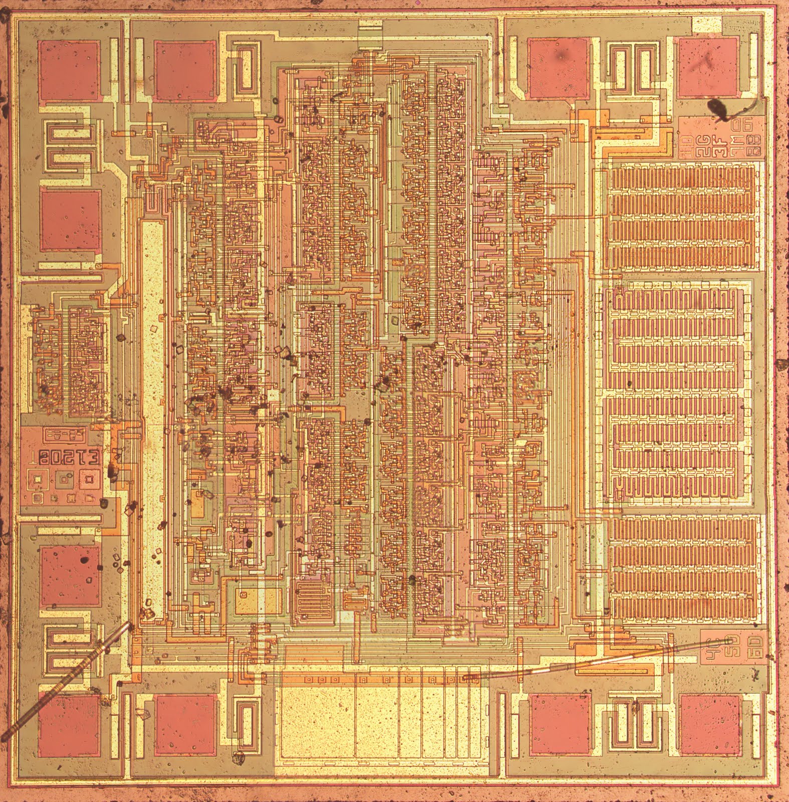
06/07/2018 at 23:28 • 0 commentsAnd a beautiful die shot !
![]()
(see https://electronupdate.blogspot.com/2018/06/digital-watch-teardown-integrated.html )
-
Small signal, high impedance amplifier
01/08/2017 at 09:54 • 17 commentsOne roadblock in this project is the oscillator circuit.
The oscillator oscillates rather well (if you accept the long power-up time) but the log Complete 18KHz source shows that there are some problems with the amplifier.
The single-MOSFET oscillator is very very sensitive to outside influences. The 10x probe doesn't affect it too much with the low capacitance and the 10M impendance but the gate of a MOSFET is something else, particularly the BS170 with 20 to 40pF that is coupled to whatever is in the circuit. So far the whole module doesn't work.
In the previous related log, I suggested a differential pair, which is a very interesting topology that I also study for #Germanium ECL and other BJT-based projects. I have found a very interesting description at https://en.wikibooks.org/wiki/Circuit_Idea/Revealing_the_Truth_about_ECL_Circuits that brings some more ideas to the table.
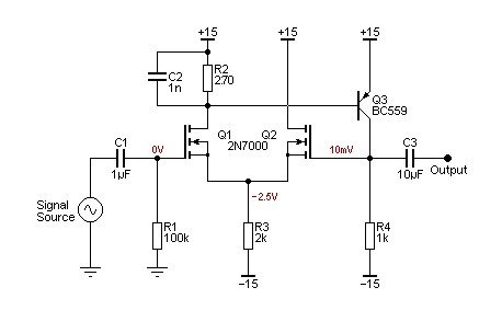
An interesting circuit:
Figure 13A - 'Ideal' Voltage Follower Using MOSFETs(courtesy of Elliott Sound Products)
but the feedback transistor should be a N or P-FET instead of PNP. I'm not sure how I will manage that.
Another chance find (it took a few days to realise) is inpired by the "tetrode" MOSFETs, such as the BS1012 (that's another story for later). While searching for informations about them, I found this page : http://www.radio-electronics.com/info/data/semicond/fet-field-effect-transistor/dual-gate-mosfet.php
"In effect, the dual gate MOSFET operation can be considered the same as two MOSFET devices in series. Both gates affect the overall MOSFET operation and hence the output."
I see this as a single-die AND gate but there is more to this part !
"The cascade amplifier helps overcome the Miller effect where capacitance is present between the input and output stages. Although the Miller effect can relate to any impedance between the input and output, normally the most critical is capacitance. This capacitance can lead to an increase in the level of input capacitance experienced and in high frequency (e.g. VHF & UHF) amplifiers it can also lead to instability.
The effect is overcome by using a cascade amplifier using a single dual gate FET. In this configuration, biasing the drain-side gate at constant potential reduces the gain loss caused by Miller effect. The effects of capacitive coupling between the input and output are virtually eliminated."
Reduced Miller effect ? That's interesting ! But what about coupling with other nodes ?
"Effectively a cascade amplifier is a two-stage amplifier formed from a trans-conductance amplifier which is followed by a current buffer. This provides a high level of input-output isolation, high input impedance, high output impedance, higher gain or higher bandwidth when compared to a single stage amplifier. "
Now this is interesting and gives a clue about how to design an equivalent circuit !
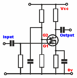
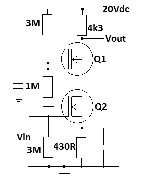
Another explanation at http://electronics.stackexchange.com/questions/69300/how-does-a-dual-gate-mosfet-reduce-miller-effect provides this diagram:
![]()
The voltages and resistor values must be changed and experimentally tested...
There is one interesting conclusion to draw for the "high impedance amplifier" case : there are at least 2 transitors
- in series (for the trans-conductance case shown above)
- in parallel (for the differential pair)
That's two topologies that I have to test and compare !
-
More minimodules
12/15/2016 at 18:51 • 0 commentsHopefully, I'll have a first system in June 2017. I hope to build it with the kids of CercleJ, where I teach electronics to teens.
The subject of this log is : let's also design square-inch sized modules that perform boolean logic, like "discrete gates", but instead of just soldering a LS/HC chip, I simply put BS170/BS250. I imagine the following gates :
- (N)AND
- (N)OR
- X(N)OR
- debounce
- (any idea ?)
This would let the kids play with logic circuits they have built themselves, instead of using a "ready made black box". We could play with the counters and all their configurations, for example.
Note that all the circuits provide both positive and negative levels, both for "practical" reasons and for directly driving the 10TFF modules.
-
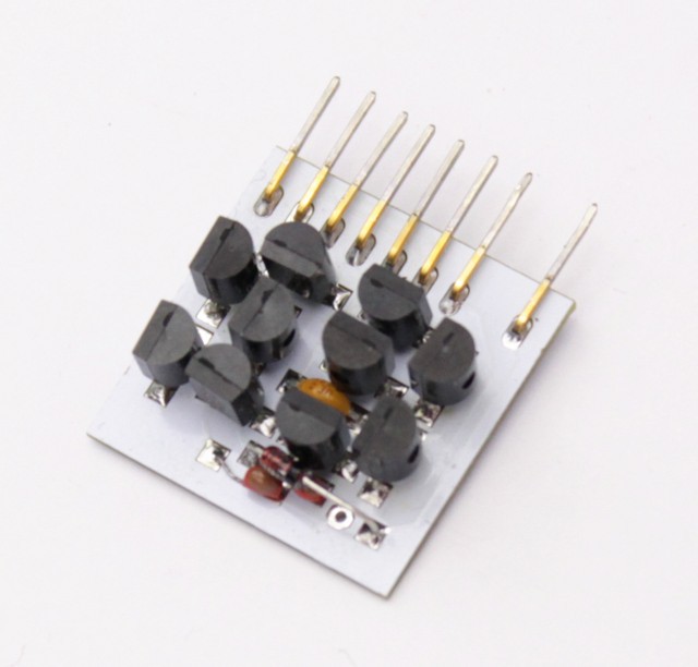
10TFF-v2 received !
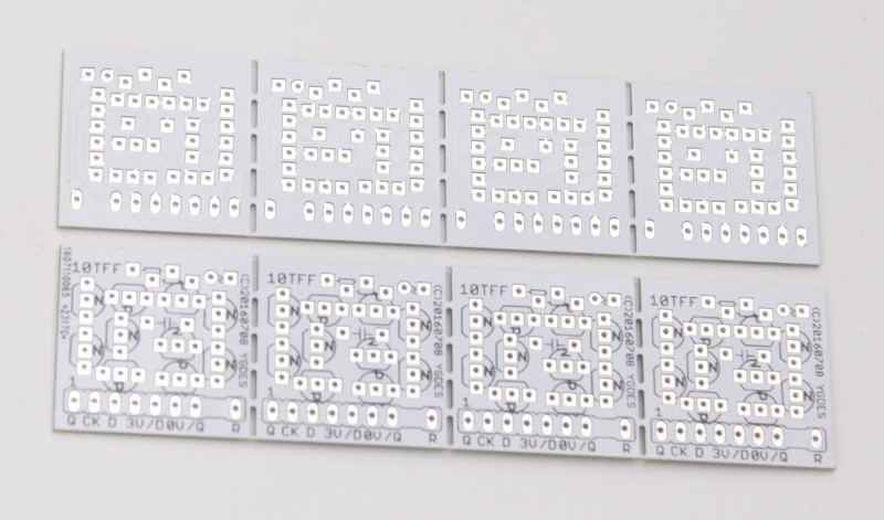
08/03/2016 at 18:01 • 4 commentsOnce again I got a great result with the batch I submitted to DirtyPCB. This time I chose a larger PCB (100×100mm) to test my idea of a universal module. I could fit 8 10TFF modules in one half of the PCB surface.
Now I have to solder a few and test them :-)
update 20160804:It appears that the distance between the pads of the axial capacitor is too short. I modify the component in Eagle to widen the gap and reduce the force on the pins.
The other weird thing is that both types of transistors have a reversed pinout. The BS170s are non-conform and this time, I try the 2N7000 with its reversed pinout. It becomes too complex to plug all the parts in reverse so for this test, I soldered the parts on the other side of the PCB. The outlines still match the parts but on the other side...
Another little change is the resistors values : this time I try with 120K, which should reduce power consumption AND operating frequency, for the slower parts of the clock.
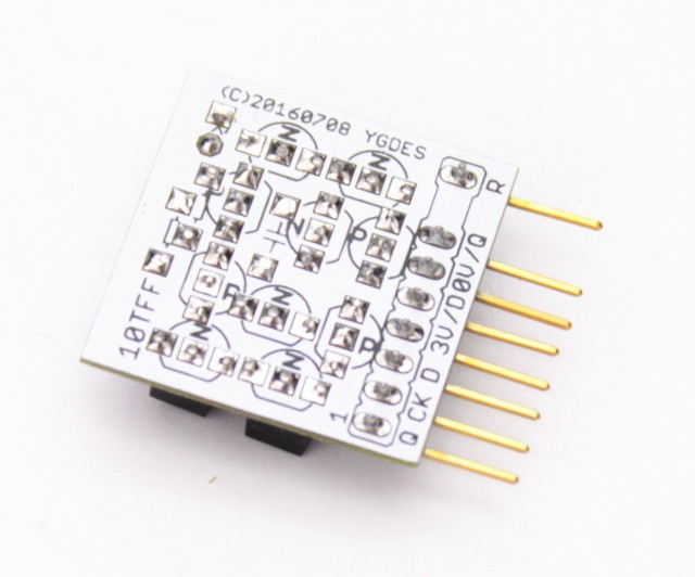
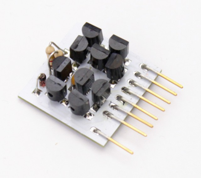
Here is a pretty "usual" module :
This one is a bit special because the 1N60 diode is connected to the other resistor and resets the latch to the opposite value:
Only one is required in the whole system but it's good to test it. Indeed, I should start to implement and test the mod3, mod5 and mod6 counters...
-
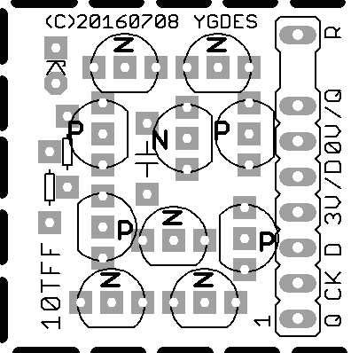
10TFF module v2
07/08/2016 at 07:55 • 0 commentsI just submitted a new PCB job for the 2nd version of the 10TFF module.
![]()
I found a short in the precedent version, fortunately I could submit a correction :-)
I also found a solution to the reset problem. The 24H board has a 3-stages 1-hot shift register instead of a 6-stages Johnson counter. There are 2 differences: the outputs are swapped for the Johnson counter and the 1-hot has one 10TFF reset to state 1. Swapping is determined by jumpers on the HMS boards but reset to 1 has been a bit tricky. The solution is simple in the end: one 10TFF module has specific wiring of the diode, which is connected to the complementary signal. The module is already too crowded to allow the modification but it's easy to rewire just one of the modules with a short wire.
The swapping of the 3-stages shift register will be selected with solder pads.
-
Complete 18KHz source
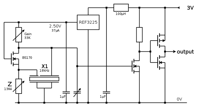
05/29/2016 at 22:39 • 0 commentsThe complete 18KHz clock source is there :
![]()
Now I must
- Build the prototype
- validate all the parts' values (easy)
- verify the frequency and tune oscillator to the best possible precision (but my Rb source fried and my DDS is far from alive :-( )
- place & route the PCB
- find a temperature controlled oven/freezer to plot the stability
Update (20160531): With the given resistor values and the REF3225, the oscillator starts within 30s, before fine-tuning !
However the output swing of the oscillator is too low (0.5V-1.5V) to properly trigger the first amplification stage. This is solved with a P-channel MOSFET instead of a N-channel :-)
Update (20160629) : the P-MOSFET works much better than the N-MOSFET but... new problems appear. I get really weird waveforms and interactions with the oscillator, some unexpected nasty (capacitive) coupling must be at work.
The ideal solution would be a JFET but this is "not kosher" for this project, I have to manage amplification with a very high input impendance and low input capacitance.
In the #Active scope probe with no dedicated power supply project, I evaluate differential amplifiers but they use JFET at the input and probably draw more than the 37µA of the primary oscillator.
How can I shield the primary osc. from the gate capacitance of the amplifier ? @K.C. Lee suggested in a previous log (https://hackaday.io/project/9376-yet-another-discrete-clock/log/32117-crystal-oscillator-with-complementary-mosfets) to add a 100K series resistor.
The bias is another issue : what is best for the oscillator is not best for the amplifying stage. A capacitive coupler is required, driving a self-biased NOT gate (P & N-MOSFET). Additional resistors at both sources might further shield from capacitances... The first stage will end up with 4 resistors, 2 FET and 1 capacitor. The coupling capacitor must be around 1nF, which gives a RC time of about 100µs, or 10KHz.
The NOT gate could be preceded by a common-drain amplifier (?) or one of the circuits described in this "booster" article.
Sorry, no drawing yet because (oh well, don't get me started)
-
Prescaler mod 5
05/28/2016 at 08:40 • 2 commentsThe "KCL structure" (covered there) is such a nice, regular circuit but it requires a mod 5 prescaler to convert the 18KHz source to 3600Hz. I have tried to make such prescaler but I was not satisfied.
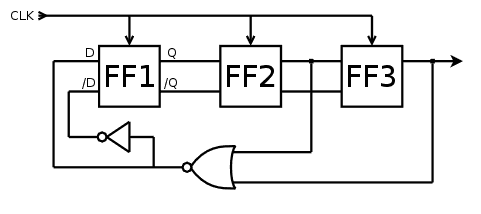
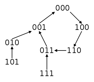
5 is such an "inbetween" number, just after 4 (which requires 2 FlipFlops) and 6 (which requires 3 FF but is very easy to do with a Johnson counter). The previous approach with a reset adds nagging timing issues. So I went back to the sketchbook and made a few diagrams. I ended up with the following circuit with 3 10TFF and one NOR gate (with complementary output).
![]()
This is not an absolutely minimal circuit, when counting transistors, but it's simple and totally synchronous, which reduces problems and debugging at high speed. No reset is needed, which also simplifies the design, and it gracefully recovers from errors.
This is actually a "modified Johnson counter", I started with a mod 6 counter and removed one state.
1 2 3
0 0 0 #0
1 0 0 #1
1 1 0 #2
1 1 1 #3 => removed
0 1 1 #4
0 0 1 #5
The new succession of states becomes:
1 2 3
0 0 0 #0
1 0 0 #1
1 1 0 #2
0 1 1 #3
0 0 1 #4
Now notice that the state 1 is added in FF1 only when FF2 and FF3 are 0. Yes, it's a NOR gate !Drawing the complete state machine gives the following diagram:
![]()
The absence of forbidden state (as in a LFSR) or subcycles of lower size makes a RESET input useless.
Implementing a NOR gate requires 2 P-FET and 2 N-FET, the inverter adds another complementary pair so the "cost" is 6 transistors. It's not the absolute best solution but I think it's so elegant that I adopted it :-)
-
Power supply for the quartz oscillator
05/27/2016 at 01:54 • 0 commentsThe new oscillator works well but it is quite sensitive to the power supply's voltage. A change of 0.1V requires the trimmers to be re-tuned.
A very good voltage regulator is necessary to preserve the frequency accuracy. This is the only exception to the "no IC" rule I've set myself.
Initially I have chosen 2.5V because there is 0.5V of margin from the 3V input supply and it's easy to obtain with the LM4041-ADJ shunt regulator (a pair of resistors of identical values increase the 1.25V output to 2.5V). The goal is to have a stable, temperature-independent voltage for the oscillator to reduce long-term drift. But it's not so easy in practice.
The LM4041 needs 60µA and draws more from the shunt operation. This is getting ridiculous because the oscillator draws less than 40µA. Overall, the power consumption is more than doubled!
One solution is to use a voltage regulator in SOT23, for example, though these chips are designed to handle more current, while absolute voltage accuracy is a second thought. I should instead use a micropower 2.5V voltage reference !
Digging in my old collection of samples (they were gathered to experiment with voltmeter accuracy) I find the following parts:
- REF3125 (Thank you TI!)
- REF3225 (Thank you TI!)
- MCP1525 (Thank you Microchip!)
- MAX6002 (Thank you Maxim !)
Speaking of current, the 3 first references are rated around 100µA, which is more than the LM4041 alone, but without the hassles of calculating the series resistor of the LM4041, which risks drawing even more current when badly chosen, so this is equivalent. There is no risk of losing regulation, if the input voltage drops dangerously low, and the current draw is almost constant.
The MAX6002 has a 100ppm/°C tempco, which is too much, despite the lowest current needs (45µA). I only have 2 samples so I can't go far and it's ruled out. Same for the bigger brother MAX6102 (only 1 sample left) with a bit more stability but more current as well (90-120µA)
The MCP1525 draws about 100µA (90µA typ. according to the datasheet, around 80µA@3V@25°C). The tempco is better (27ppm typ. at full temperature range) and I got 5 samples, I can go further than with Maxim.
The REF3125 has more samples left (7) and has better drift performance (15 ppm/°C max, 5ppm typ at ambient temperature). Noise characteristics are important too : 48 μV RMS from f = 10 Hz to 10 kHz but we'll talk about it later. Quiescent current is announced around 100µA (typ.@25°C). Sounds good.
Now the more recent REF3225 has 10 samples left, maybe because in the past I might have been afraid of the SOT23-6 package. It's still drawing around 100µA but the drift is typically 4ppm/°C. This is stable ! It seems that this is the winner.
If you have better suggestions, please contact me and/or send me samples!
Noise is another thing. Voltage references are noisy. I learned it the hard way, for an audio project, but here, I'm not doing a VHF, ultra-low-jitter oscillator. As long as the frequency is stable over the long term, I'm fine.
So, filter or no filter ? The power supply/input must be filtered with a LC cell to prevent switching noise from disturbing the clock. The output however is something else. I am tempted to over-filter it but this might not be the most efficient approach. The noise might actually help the oscillator to startup faster and the reference might react to the changes in load, which could actually help.
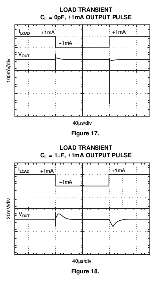
Looking at Fig.17 and Fig.18 of the REF3225's datasheet, I'm tempted to add a small capacitive load to make a long enough "bump" that helps with the startup.
![]()
On the contrary, without capacitor, the change in load will make a very short spike that will not bring some rebound to the quartz.
I'm thinking about this because the goal is to startup faster, if needed with the help of an external device or button. I still have to experiment with a shorting MOSFET.
It must be noted that these parts work with light or even no load. It shouldn't be a problem to draw only 37µA, unlike other larger regulators.
- REF3125 (Thank you TI!)
-
Success ! a minimalist, single-MOSFET quartz oscillator !
05/26/2016 at 21:10 • 4 commentsMy quest is finally over !
I didn't believe it when I wrote Impendance matching for crystal oscillators but I had to try it and it worked !
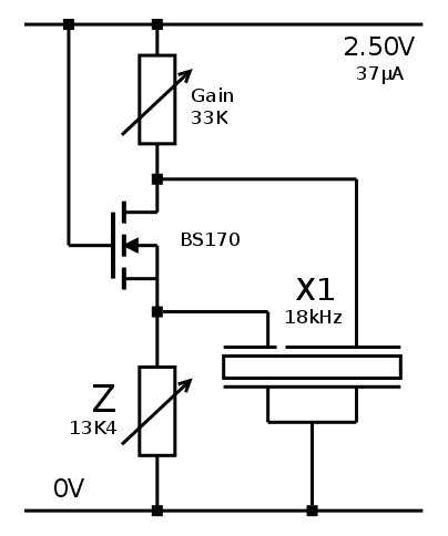
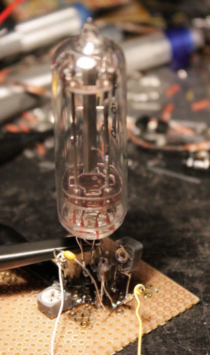
![]()
This circuit fits all my requirements:
- works at low voltage, below 3V, so I can use a micropower voltage regulator
- low power (I just measured it : 37µA only, less than 100µW !)
- minimal parts count : beside the crystal resonator, only a MOSFET and a couple of adjustable resistors (to be changed when voltage is modified)
Yes, only 3 additional parts (not counting the decoupling capacitor), my precedent theory seems to work !The downsides are a) slow/lazy startup and b) 3rd harmonics but they are not critical flaws.
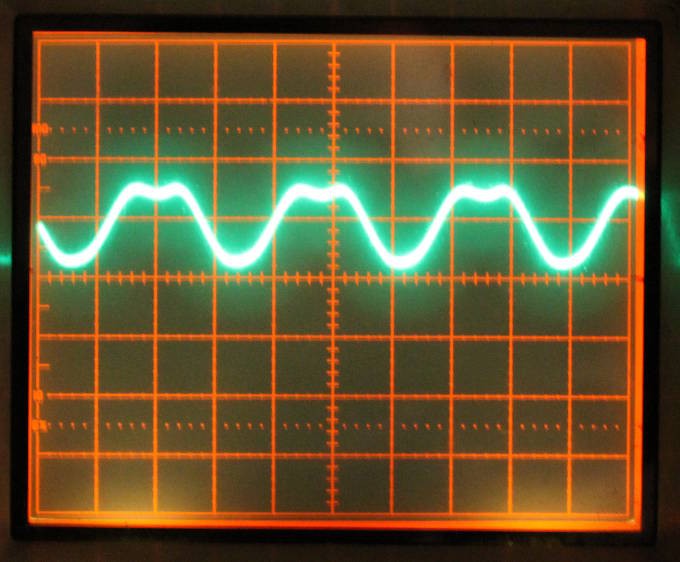
(trace: 1V/div)The resistors need some tuning to adjust the waveform amplitude and offset but nothing too hard thanks to a simple 'scope. I don't see how to reduce the 3rd harmonics but I don't care much now.
I wish I knew a better way to start the oscillation than tapping it.
TODO:
- Test with 2N7000
- Tune to exactly 18000.00Hz
- Design a proper output stage/buffer
- Something something
- Profit ?
-
Impendance matching for crystal oscillators
05/26/2016 at 01:35 • 7 commentsI think I understand better now.
Many of my failed attempts are due to another condition that I didn't check, and which comes from one fundamental difference between MOSFET and BJT : there is no current going through the gate.
There are two "working" BJT circuits that use a pair of transistors and one in particular works great, even with "lazy" PNP such as the OC70: the "capacitor-coupled amplifier":
![]() In It just works I reported that the circuit works very well but in Another MOSFET oscillator I saw that it's not possible to translate it directly to MOSFET.
In It just works I reported that the circuit works very well but in Another MOSFET oscillator I saw that it's not possible to translate it directly to MOSFET.I now see what was wrong with my attempts : the BJT oscillator lets signal/current flow through the crystal, thanks to the current path from base to emitter. When I use MOSFETs, something is missing, the "driver" transistor "shakes" on pin of the crystal but the other pin is floating and can't let the equivalent LC network oscillate. No energy is input because the other pin is floating and no energy goes out.
More important : the equivalent resistance, the impedance, is critical to allow the oscillations. All the crystal oscillators I've tried start to oscillate, or oscillate better, when one of the resistances is at a very particular value. It's the impendance matching part of the equation.
In the classic Pierce oscillator with inverter, the impendance is set with a series resistor and the two "parallel" capacitors. The last capacitor (connected to the inverter's input) is the critical one, which connects the signal to the ground so the crystal doesn't dangle in the void. My error becomes pretty apparent in the log Crystal oscillator with complementary MOSFETs where the capacitor is missing, the crystal pin is virtually dangling with no return path for the current !
So now, one design parameter or constraint is : the resonating element is not only the crystal, but also a resistor in series with the crystal.
- One of the parts is connected to a stable voltage, such as ground (ideally) or Vcc.
- The other end is connected to the "driver" transistor's output
- The middle point is where the "sense" gets the signal.
Let's add that the circuit must work under 3V and use a minimal number of parts, the new trick is to integrate the series resistor in the biasing network of the transistors. Naturally this leads to funky circuits with common gate or common drain configurations.
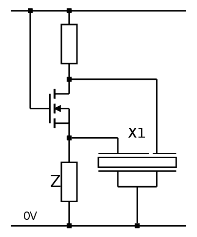
However common drain configurations have a voltage gain less than one. I somehow came up with this strange common-gate configuration:
![]()
(erratum: the crystal is wired in reverse... Sleep or hack, but don't do both)
(yes, I understand now that this can't work as is but it's a start)
According to some sources, the common gate configuration is a non-inverting voltage amplifier. The input comes from the source, where the Z resistor (impendance matching) is tied to the ground. X1 is also connected to the drain, which is the output node.
I'm not sure at all that it will work but it could... and if it doesn't, I can still try with cross-coupled pairs. Actually, Z also gets current when the MOSFET is conducting, which increases the input and "degenerates" the output. The driving strength would be lower than the typical common source, which also amplifies the current.
Since there is only one transistor (not a complementary pair), the working voltage would be in the 2-3V ballpark, depending on the resistor values.
OMG OMG OMG IT WORKS
Yet Another (Discrete) Clock
I HAD to finally do this basic "exercice de style" in digital electronics, using some hundreds of transistors and diodes...
 Yann Guidon / YGDES

 In
In 