SHAOS
SHAOS-
Board NEDONAND-16
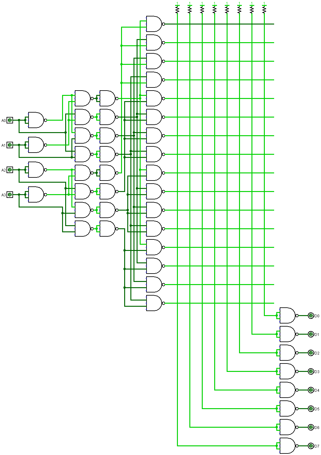
03/06/2016 at 23:01 • 1 commentThis board is 1st one for NEDONAND project that was done in pcb-application from gEDA, because of its size (all previous board met free Eagle size limitations). This is 16-byte ROM for NEDONAND:
![]()
In every intersection above a diode could be put and it will drive that bit of those line down if this line is active (grounded) - so board should have 16 16-pin SIP sockets in order to make this ROM "re-programmable" manually:
![]()
4-bit address is going in through 4 header on the left and output is 12-pin header up with common memory interface that I will use for all memory boards for NEDONAND:
1) GND - ground
2) D0 - output bit 0
3) D1 - output bit 1
4) D2 - output bit 2
5) D3 - output bit 3
6) D4 - output bit 4
7) D5 - output bit 5
8) D6 - output bit 6
9) D7 - output bit 7
10) /RD (connected to LED in case of NEDONAND-16)
11) /CS (not connected in case of NEDONAND-16)
12) VCC - power +5V
Board had received from OSHPark and successfully tested - now it's also shared there...
-
Revised board NEDONAND-4
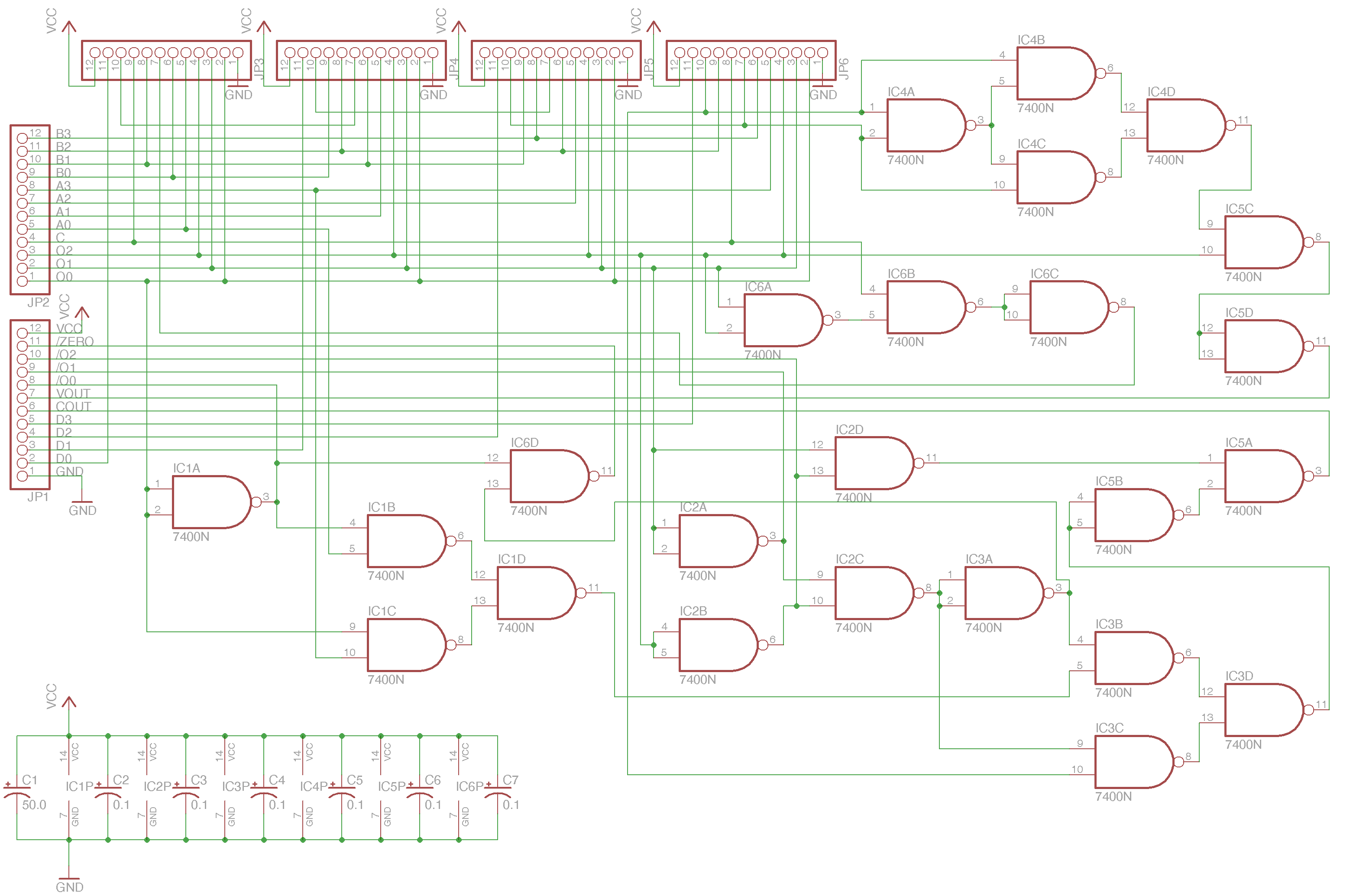
03/01/2016 at 09:16 • 0 commentsFixed some issues in previously shared NEDONAND-4 board:
![]()
Recreated in Eagle:
![]()
And ordered through OSHPark:
![]()
Pin description:
1.1) GND - ground 1.2) D0 - output data bit 0 1.3) D1 - output data bit 1 1.4) D2 - output data bit 2 1.5) D3 - output data bit 3 1.6) COUT - output of carry/borrow 1.7) VOUT - output of overflow 1.8) /O0 - inverted O0 (just in case) 1.9) /O1 - inverted O1 (just in case) 1.10) /O2 - inverted O2 (just in case) 1.11) /ZERO - "0" if operation is 000 1.12) VCC - power +5V 2.1) O0 - operation input bit 0 2.2) O1 - operation input bit 1 2.3) O2 - operation input bit 2 2.4) C - carry/borrow input 2.5) A0 - first argument bit 0 2.6) A1 - first argument bit 1 2.7) A2 - first argument bit 2 2.8) A3 - first argument bit 3 2.9) B0 - second argument bit 0 2.10) B1 - second argument bit 1 2.11) B2 - second argument bit 2 2.12) B3 - second argument bit 3 -
Board NEDONAND-9
02/28/2016 at 19:21 • 0 commentsNEDONAND-9 is 9-input AND gate build from four 74F00 chips (16 NAND-gates):
![]()
Eagle version of it:
![]()
Board already ordered through OSHPark (will be shared after testing):
![]()
Pins: GND,A,B,C,D,E,F,G,H,I,AND,VCC (from right to left)
-
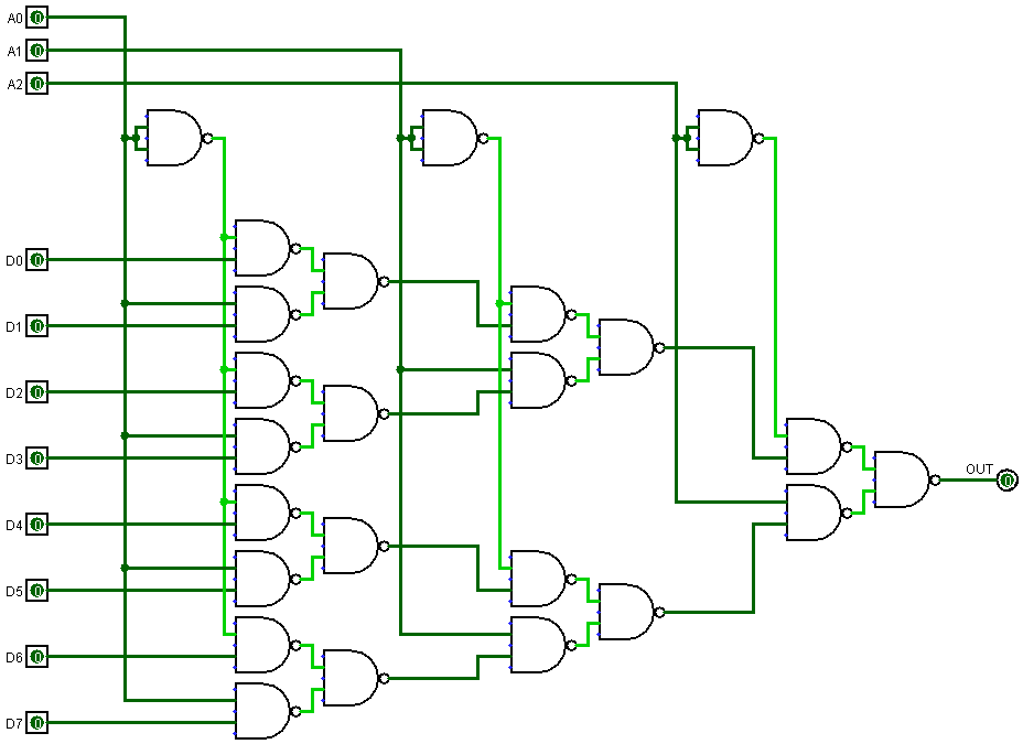
Board NEDONAND-8
02/28/2016 at 13:05 • 0 commentsNEDONAND-8 is one multiplexer 8:1 controlled by 3 address inputs - see "mux8" in nedonand.circ:
![]()
Eagle v5.12 circuit replicates the same approach:
![]()
And it's already ordered through OSHPark (but not yet shared there because I need to test it first):
![]()
Pins description:
1) GND - ground
2) I0 - input if A=0
3) I1 - input if A=1
4) I2 - input if A=2
5) I3 - input if A=3
6) I4 - input if A=4
7) I5 - input if A=5
8) I6 - input if A=6
9) I7 - input if A=7
10)OUT - output of multiplexer
11)NC - not connected
12)VCC - power +5V
13)GND - another ground
14)A0 - bit 0 of address
15)A1 - bit 1 of address
16)A2 - bit 2 of address
-
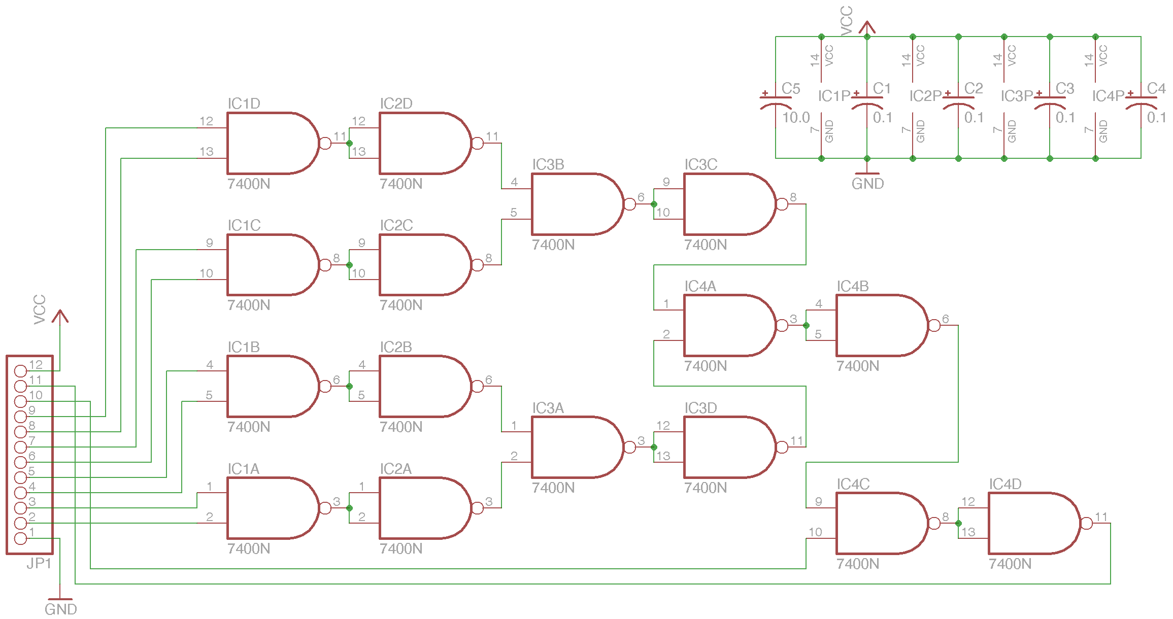
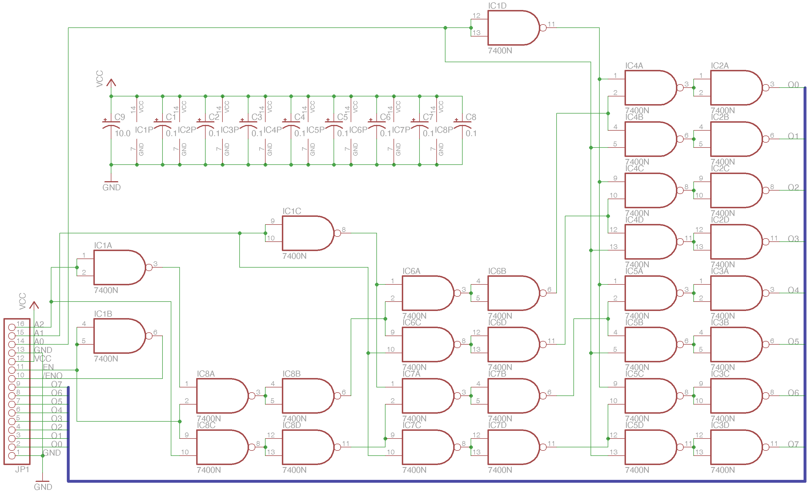
Board NEDONAND-7
02/28/2016 at 06:41 • 0 commentsBoard NEDONAND-7 implements demultiplexer 1:8 with active "1":
![]()
Input EN is also inverted and going out as /ENO for cascading. Board was already ordered through OSHPark:
![]()
Pins description:
1) GND - ground 2) O0 - output "1" if EN="1" and A=0 3) O1 - output "1" if EN="1" and A=1 4) O2 - output "1" if EN="1" and A=2 5) O3 - output "1" if EN="1" and A=3 6) O4 - output "1" if EN="1" and A=4 7) O5 - output "1" if EN="1" and A=5 8) O6 - output "1" if EN="1" and A=6 9) O7 - output "1" if EN="1" and A=7 10)/ENO - output of inverted EN 11)EN - enable input (must be "1" to demultiplex) 12)VCC - power +5V 13)GND - another ground 14)A0 - bit 0 of address 15)A1 - bit 1 of address 16)A2 - bit 2 of address -
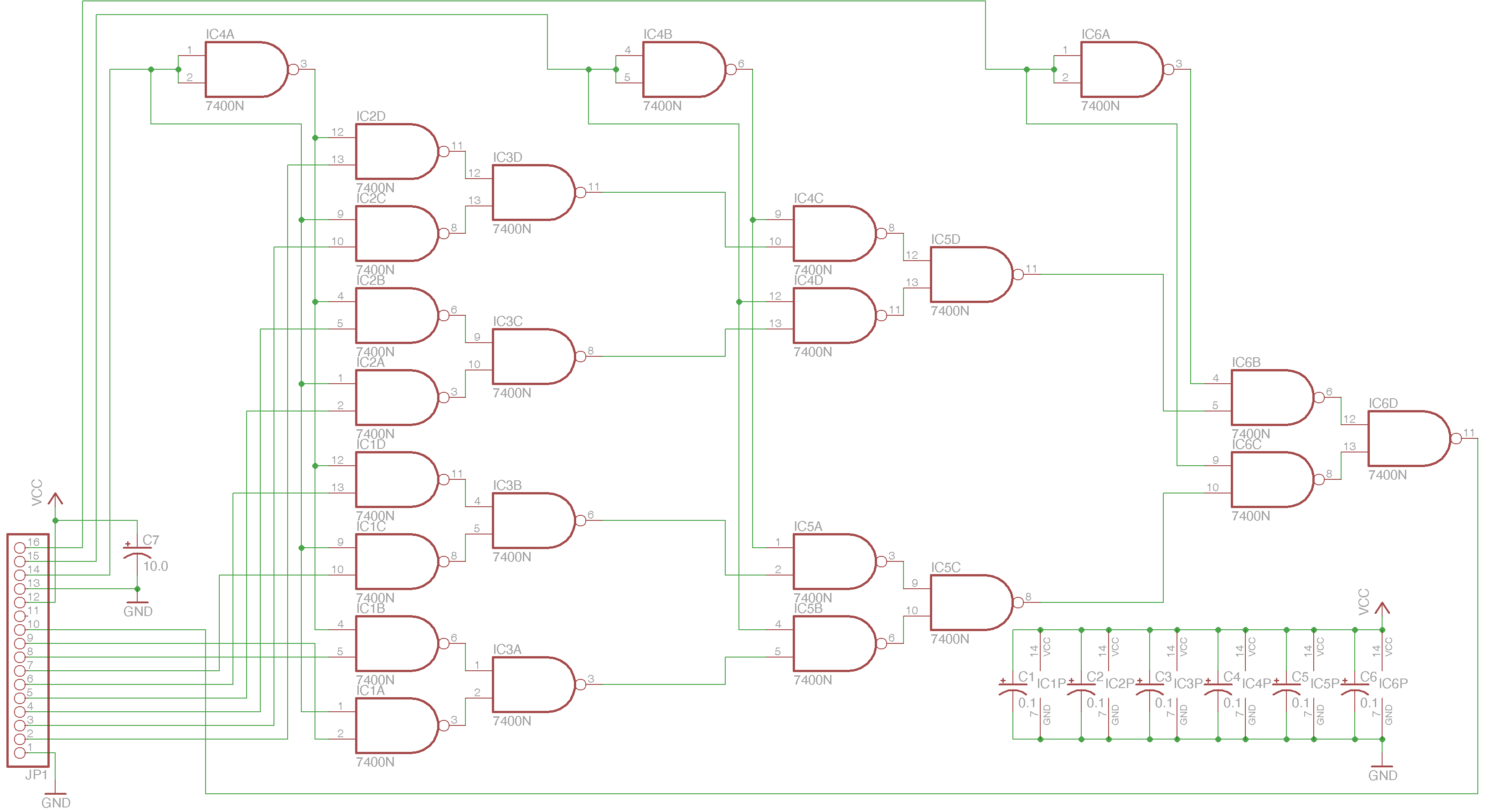
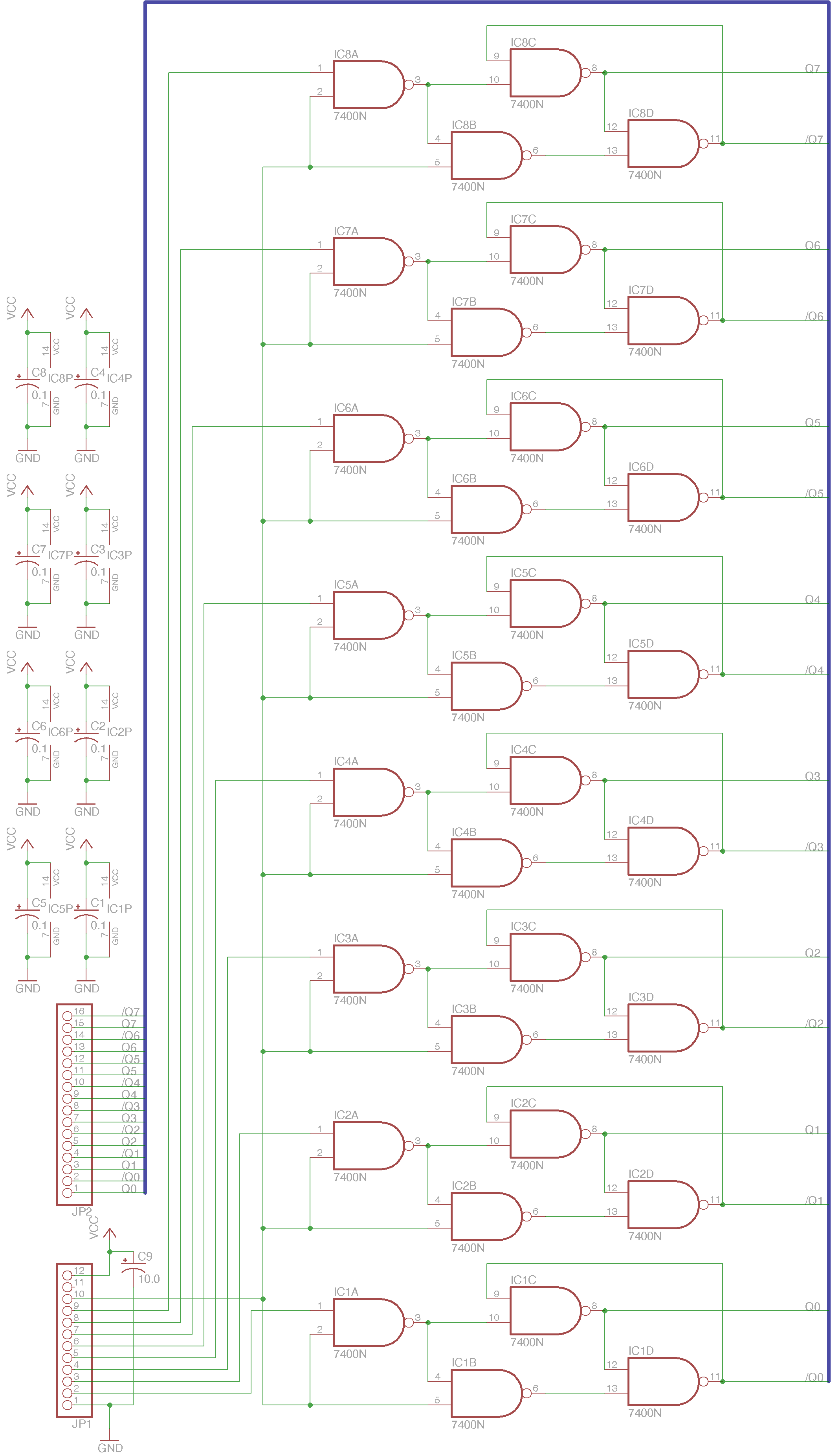
Board NEDONAND-6
02/28/2016 at 01:28 • 0 commentsNEDONAND-6 is 8 multiplexers 2:1 with common control (straight select and inverted select):
![]()
Board already ordered through OSHPark:
![]()
Pins description:
1.1) GND - ground
1.2) O0 - output of multiplexer 0
1.3) O1 - output of multiplexer 1
1.4) O2 - output of multiplexer 2
1.5) O3 - output of multiplexer 3
1.6) O4 - output of multiplexer 4
1.7) O5 - output of multiplexer 5
1.8) O6 - output of multiplexer 6
1.9) O7 - output of multiplexer 7
1.10)SEL - straight select
1.11)/SEL - inverted select
1.12)VCC - power +5V

2.1) A0 - input A of multiplexer 0
2.2) B0 - input B of multiplexer 0
2.3) A1 - input A of multiplexer 1
2.4) B1 - input B of multiplexer 1
2.5) A2 - input A of multiplexer 2
2.6) B2 - input B of multiplexer 2
2.7) A3 - input A of multiplexer 3
2.8) B3 - input B of multiplexer 3
2.9) A4 - input A of multiplexer 4
2.10)B4 - input B of multiplexer 4
2.11)A5 - input A of multiplexer 5
2.12)B5 - input B of multiplexer 5
2.13)A6 - input A of multiplexer 6
2.14)B6 - input B of multiplexer 6
2.15)A7 - input A of multiplexer 7
2.16)B7 - input B of multiplexer 7
It could be connected together with NEDONAND-5 to get 8-bit register with controlled inversion on outputs (useful for register T).
-
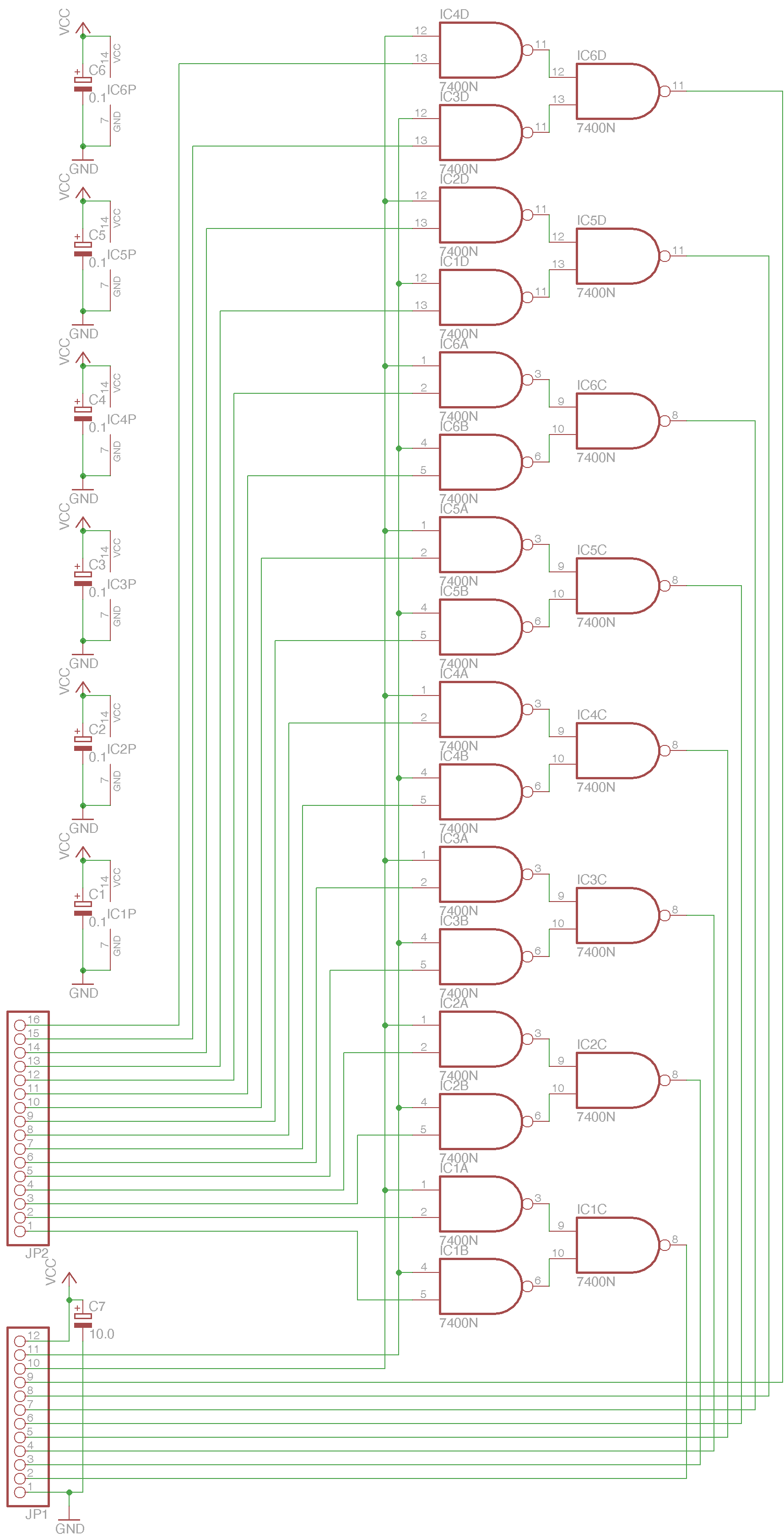
Board NEDONAND-5
02/27/2016 at 05:44 • 0 commentsThis is 5th board for NEDONAND - 8-bit register (transparent latch) with active "1" strobe with 8 straight outputs and 8 inverted outputs:
![]()
Board will be produced by OSHPark:
![]()
Pin description:
1.1) GND - ground
1.2) D0 - input bit 0
1.3) D1 - input bit 1
1.4) D2 - input bit 2
1.5) D3 - input bit 3
1.6) D4 - input bit 4
1.7) D5 - input bit 5
1.8) D6 - input bit 6
1.9) D7 - input bit 7
1.10) STB - strobe (active "1")
1.11) NC  - not connected
1.12) VCC - power +5V
2.1) Q0 - output stored bit 0
2.2) /Q0 - output inverted stored bit 0
2.3) Q1 - output stored bit 1
2.4) /Q1 - output inverted stored bit 1
2.5) Q2 - output stored bit 2
2.6) /Q2 - output inverted stored bit 2
2.7) Q3 - output stored bit 3
2.8) /Q3 - output inverted stored bit 3
2.9) Q4 - output stored bit 4
2.10) /Q4 - output inverted stored bit 4
2.11) Q5 - output stored bit 5
2.12) /Q5 - output inverted stored bit 5
2.13) Q6 - output stored bit 6
2.14) /Q6 - output inverted stored bit 6
2.15) Q7 - output stored bit 7
2.16) /Q7 - output inverted stored bit 7
This board will be used to implement NEDONAND registers A,B,C,D,E and T (temporary register) - one board per register. -
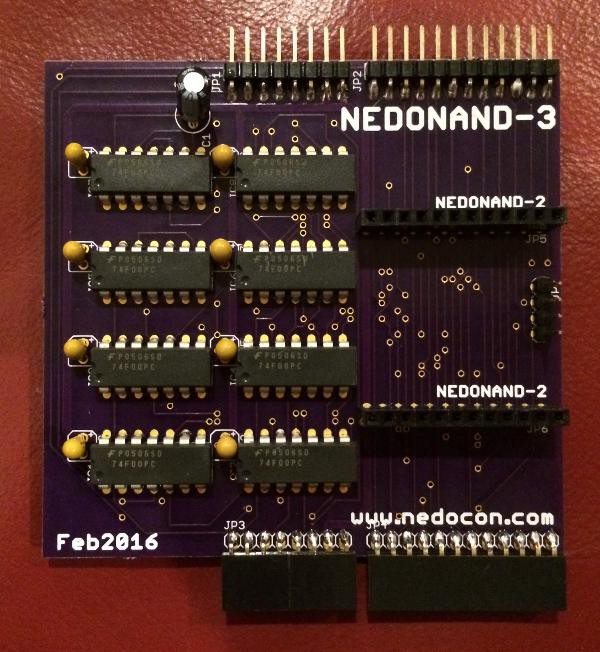
Test NEDONAND-3 with 2 boards NEDONAND-2
02/25/2016 at 14:43 • 3 commentsNEDONAND-3 is 4-bit synchronous counter with parallel load and asynchronous clear similar to 74161 chip:
![]()
This is assembled one:
![]()
This how it looks with connected two NEDONAND-2 boards (dual edge-controlled D-triggers):
![]()
So it's 26 chips 74F00 implementing a single 74161 ;)
BTW it's eating about 130 mA constantly,,,
-
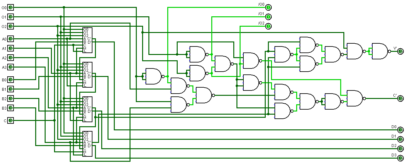
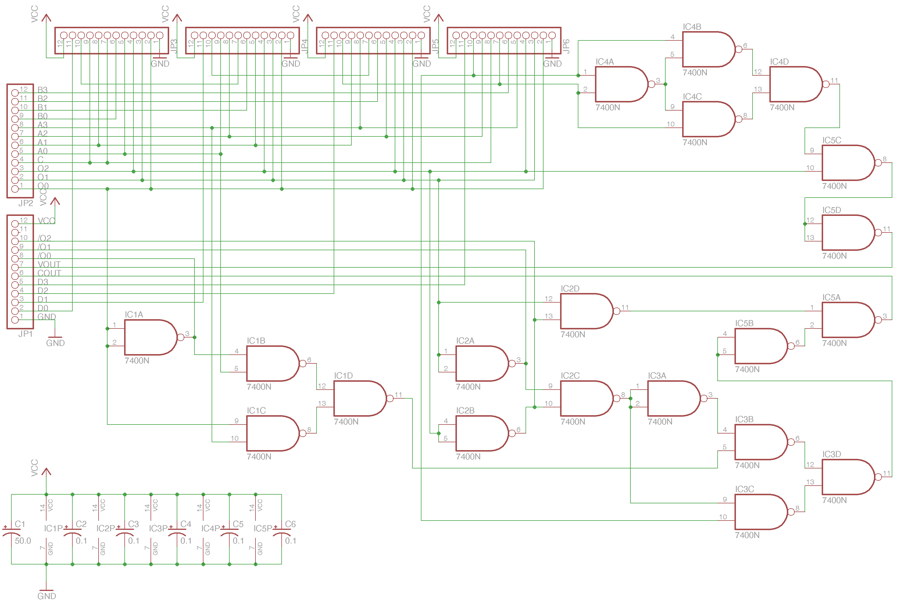
Board NEDONAND-4
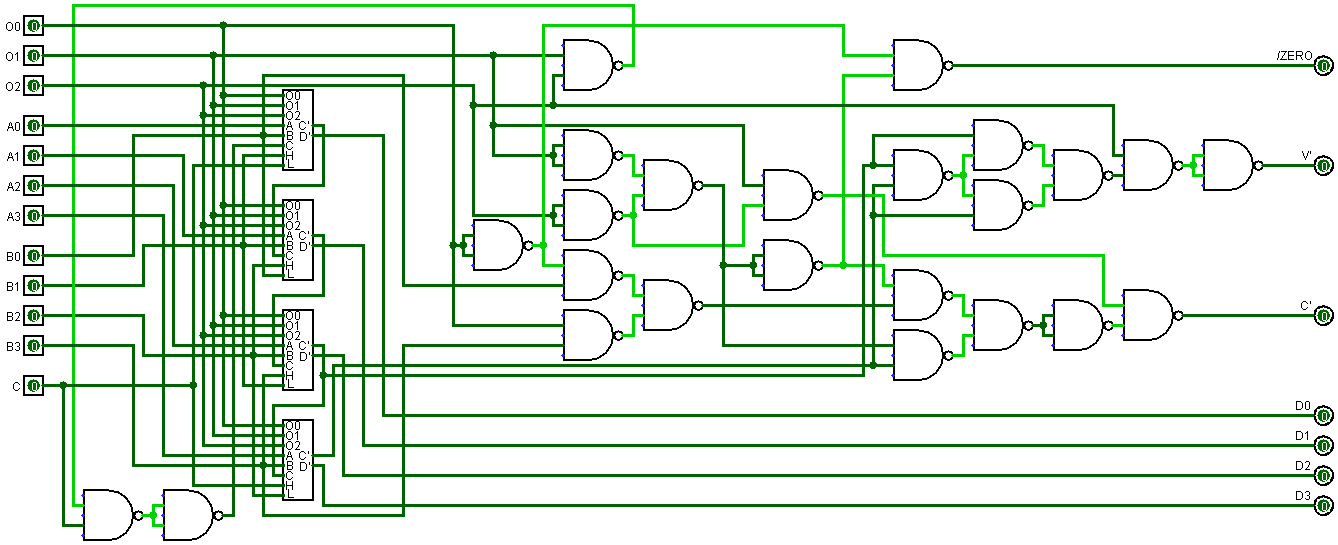
02/25/2016 at 06:04 • 1 commentI extended a little 4-bit ALU circuit to give V (overflow) output only in case of add/subtract operations:
![]()
Eagle design implementing this called NEDONAND-4 (and it uses four NEDONAND-1 boards):
![]()
Pin descriptions:
1.1) GND - ground
1.2) D0 - output data bit 0
1.3) D1 - output data bit 1
1.4) D2 - output data bit 2
1.5) D3 - output data bit 3
1.6) COUT - output of carry/borrow
1.7) VOUT - output of overflow
1.8) /O0 - inverted O0 (just in case)
1.9) /O1 - inverted O1 (just in case)
1.10) /O2 - inverted O2 (just in case)
1.11) NC - not connected
1.12) VCC - power +5V

2.1) O0 - operation input bit 0
2.2) O1 - operation input bit 1
2.3) O2 - operation input bit 2
2.4) C - carry/borrow input
2.5) A0 - first argument bit 0
2.6) A1 - first argument bit 1
2.7) A2 - first argument bit 2
2.8) A3 - first argument bit 3
2.9) B0 - second argument bit 0
2.10) B1 - second argument bit 1
2.11) B2 - second argument bit 2
2.12) B3 - second argument bit 3
Board for NEDONAND-4 was already ordered on OSHPark:
![]()
P.S. This design was revised !!!
-
Lets code a little
02/24/2016 at 05:57 • 2 commentsNEDONAND may directly addres 2Kbytes of program memory (8 bits in register G and 3 bits in register F - total 11). These are ways to jump in the code:
1) call first 64 bytes of the program memory with 8-byte steps (1 byte):
10000xxx (0=xxx - RST xxx)
2) jump to the beginning of the current 256-byte page (1 byte):10111000 (G=0)
3) jump inside of the 1st half of the current 256-byte page (2 bytes):
0xxxxxxx (A=0xxxxxxx)
10111001 (G=A)
4) jump inside of the 2nd half of the current 256-byte page (3 bytes):
0xxxxxxx (A=0xxxxxxx)
10001001 (A=~A - invert A)
10111001 (G=A)
5) jump to the beginning of arbitrary 256-byte page (3 bytes):
00000xxx (A=00000xxx)
10110001 (F=A)
10111000 (G=0)
6) jump inside of the 1st half of arbitrary 256-byte page (4 bytes):00000xxx (A=00000xxx) 00110001 (F=A) 0yyyyyyy (A=0yyyyyyy) 00111001 (G=A)
7) jump inside of the 2nd half of arbitrary 256-byte page (5 bytes):
00000xxx (A=00000xxx)
10110001 (F=A)
0yyyyyyy (A=0yyyyyyy)
10001001 (A=~A - invert A)
10111001 (G=A)
Note: value for inversion should be calculated by assembler as 255-A (where A=128...255)
NEDONAND homebrew computer
NEDONAND is 8-bit homebrew computer entirely built out of many 74F00 chips (2-input NAND gates)