E. N. Hering
-
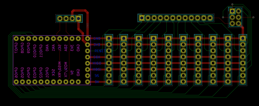
The backbone.
09/13/2016 at 01:24 • 0 comments![]()
This is the first version of the system backbone. The MCU modules will be plugged to this PCB. The MCU module footprint present on the board is there to receive the communications module, which calls each of the plugged modules, sending or receiving data depending on the module function. In this board is also present a ISP connector to program each module separately and a 12 pin header that will connect the ISP reset to the RESET of the module that will be programmed. Finally, a 4 pin connector is also present, connecting the COM module with the wifi transceiver, via a serial connection. All this information in only one paragraph sounds confusing, I know. If you have questions, please ask. As always, comments are welcome.
-
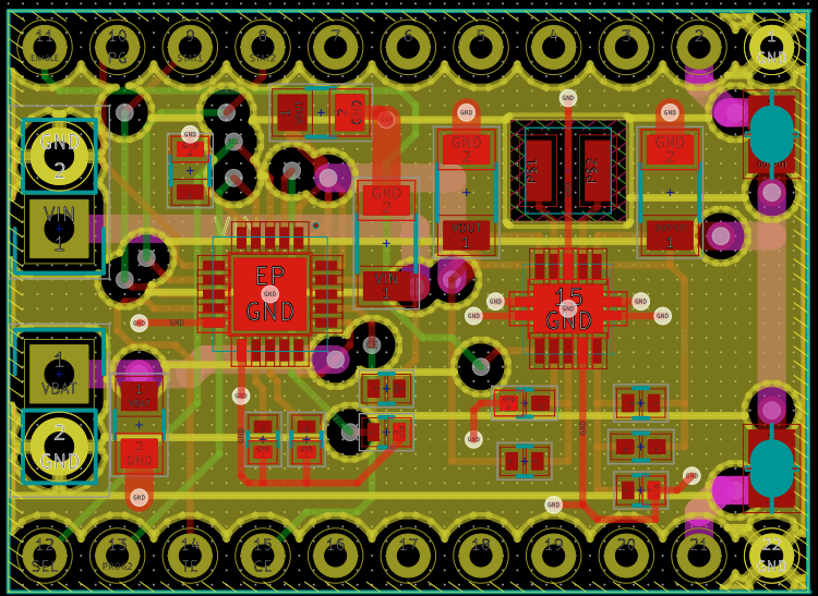
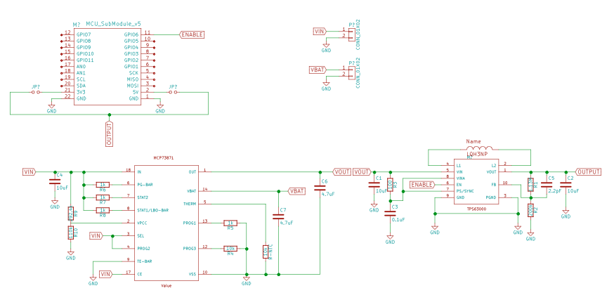
Power supply submodule.
09/12/2016 at 02:40 • 0 comments![]()
This is a candidate for the power supply submodule. Its diagram is here:
![]()
Comments are welcome.
-
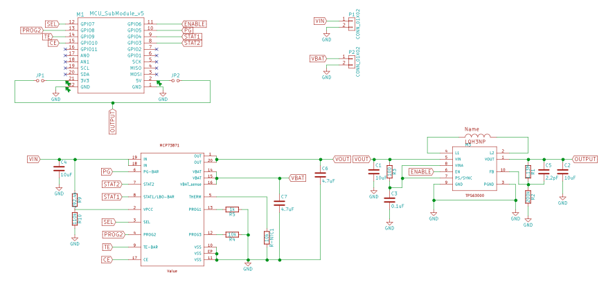
PS Correction.
09/11/2016 at 01:55 • 0 comments![]()
This PS schematic is better. It includes the control lines PG, STAT1 and STAT2 on the submodule connections. This PS is also a LiPo charger. It should be able to switch seamlessly between output power (VIN) and battery power (VBAT), charging the battery when VIN is present.
-
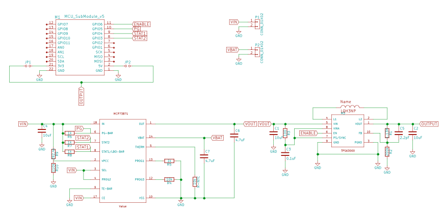
Power Supply submodule.
09/11/2016 at 01:40 • 0 comments![]()
This is the power supply. In the new version (v5) it will be placed in a submodule and connected to a MCU module. The MCU will be able to monitor and control the PS. Please comment.
-
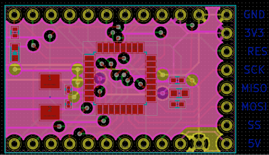
New MCU module.
09/10/2016 at 18:24 • 1 comment![]()
Ok. This is the new MCU board, populated with an ATMega328P. It follows the v5 standard. Please comment.
-
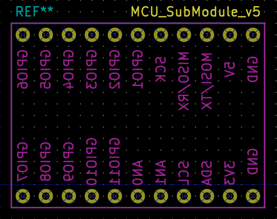
New MCU submodule standard
09/08/2016 at 15:21 • 0 comments![]()
And this is the new candidate for the submodule standard v5. All submodule components must fit inside it and use the upper and lower connections to connect to the MCU module. Please comment.
-
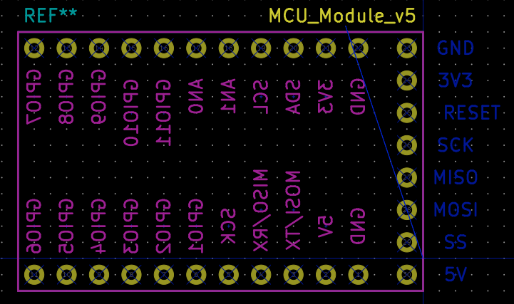
New MCU module standard
09/08/2016 at 14:49 • 0 comments![]()
This is my candidate for a new standard for the MCU module. A 5V pin was added to the right connections, which are plugged to the main bus. The upper and lower connections were rearranged, organising the pins in groups per function and making it easier to change the ATMega328P MCU for another one, while keeping the connection standard to the submodules. This module is one pin larger than the last one. Please comment.
-
Pausing everything
07/02/2016 at 21:59 • 0 commentsHi everybody!
I'm pausing the development of this project for a while. My daughter will be born in the next days and I've been dedicating all my time to the event. In the meantime, please visit the project website: www.labvant.com where you can find most of the information. I'm also keeping an IRC channel open to chat with everyone interested in pushing the development further.
-
The project name is not good.
05/20/2016 at 10:59 • 0 commentsCan you help me finding a better one?
-
Website update
05/17/2016 at 20:45 • 0 commentsThe labvant.com website has been updated. A new repository has been created for each module. A new repo dedicated to the firmware has also been created. I'll start moving the files from my private repo to the new locations tonight.
Modular Unmanned Vehicle Controller
(former YAUVeC - Yet Another Unmanned Vehicle Controller)