Close
0%
0%

AMBAP: A Modest Bitslice Architecture Proposal

Trying to unify and simplify a minimal architecture for various implementation technologies...

Similar projects worth following
A modest proposal for a simple, scalable, easy to implement bitslice architecture.
Can be used with relays, germanium or silicium transistor, DTL, DCTL, TTL, CBJT, ECL, CMOS...
Each slice implements all the necessary functions of a datapath, its distinctive feature is that the register set is merged with the selectors and the ALU. The control (decode and sequence) unit is still separated from this single-bit datapath, leaving the instruction format unconstrained.
The complexity of each slice is easy to estimate so the word width can be chosen depending on the available resources.

I started from the very beginning, with a relay implementation, but I forked this to #YGREC16. Now I'll try to focus on architectural/structural/user-visible features and design methodology, to create a new "canonical RISC" architecture.

This project was not initially meant to become a high-performance processor, but a generic tile, like the am2900 bitslice or the 74LS181 chips.

The difference, though, is that this slice is really one bit wide and each slice/module includes the necessary registers. Actually, it's an extension of the #SPDT16: 16-bits arithmetic unit with relays datapath, with logic functions added, and more registers.


The first implementation is with relays : #YGREC16 - YG's 16bits Relay Electronic Computer (moved to #YGREC-РЭС15-bis)

Faster versions with Germanium, Silicium and CMOS are in the works, and other technologies should appear later. For example, it's also a good candidate for an ASIC implementation :-)

A smaller core, the byte-wide #YGREC8 might even be the first to become operational in FPGA then with #Shared Silicon...

The "AMBAP" principles are the heart of the YGREC microcontroller family and the foundation for the redesign of #F-CPU. The #YASEP Yet Another Small Embedded Processor already pioneered many of these ideas.


This is the result of a thought experiment : as I wanted to design discrete computers with various technologies, it was hard to estimate how many gates, transistors, relays, or parts, would be required. How many elements should I buy to reach a given level of functionality ? If I can acquire X parts, what am I able to build and what will be the performance ? What will be the datapath width, instruction set and capacity ?

Dieter went through the same thought process before me: "Second: It turned out to be hard to estimate the size of the CPU (or the number of transistors)." so he built a TTL machine...

The solution I found is a set of recipes :

  1. Forget about the instruction set. It's a distraction. First, design the computing elements then wrap them around suitable control logic when the computational datapath is ready. Good old RISC principles will do the rest. Like, keep everything dumb, orthogonal and 1-cycle.
  2. Only include the vital circuits to perform Add/sub-related instructions, ROP2 and some shift. Keep the critical datapath short and simple. Multiplies, division, barrel shifter and anything else belong to external, slower units (with potential for pipelining).
  3. You basically need to care about the following fundamental circuits : MUX (MUX2, MUX4, MUX8), XOR, latch and/or DFF.
    Actually, once you have a MUX, you're almost done since you can do everything with a MUX !
  4. Focus on only one bit of computation and make it a tile that you can copy-paste at will. This way, you have a rough formula, depending on the number of registers and datapath width, that helps you tune your computer's size. It will appear quickly that 8 or 16 registers is a "sweet spot" but it can be changed at will.
  5. Register-mapped memory increases the number of necessary registers but saves a lot of complexity. It also makes the architecture more scalable and increases performance, with simultaneous accesses from separate arrays. I've solved the fundamental issues with the #YASEP Yet Another Small Embedded Processor so go for it. You can mix&match the configuration of the memory blocks according to your needs.
  6. PC as a general purpose register : usually required for general-purpose computing, you can keep it separate for special architectures (this saves one register, particularly if register addressing space is constrained). OTOH, a unified register file saves opcodes. So the rule of thumb is : PC is a user-visible register for 16 registers or more.
  7. Don't let yourself get caught in a nightmarish forest of control signals : it's nice to predecode as much as possible but high fanout signals can make the design impractical ! Find a compromise between local and global decoding. This varies from technology to technology...

Once you have good estimates of the complexity of each gate and circuit, you can estimate the cost/complexity/size of the bitslice and tune the parameters.


Logs:...

Read more »

  • Back in the days

    Yann Guidon / YGDES12/14/2018 at 19:44 0 comments

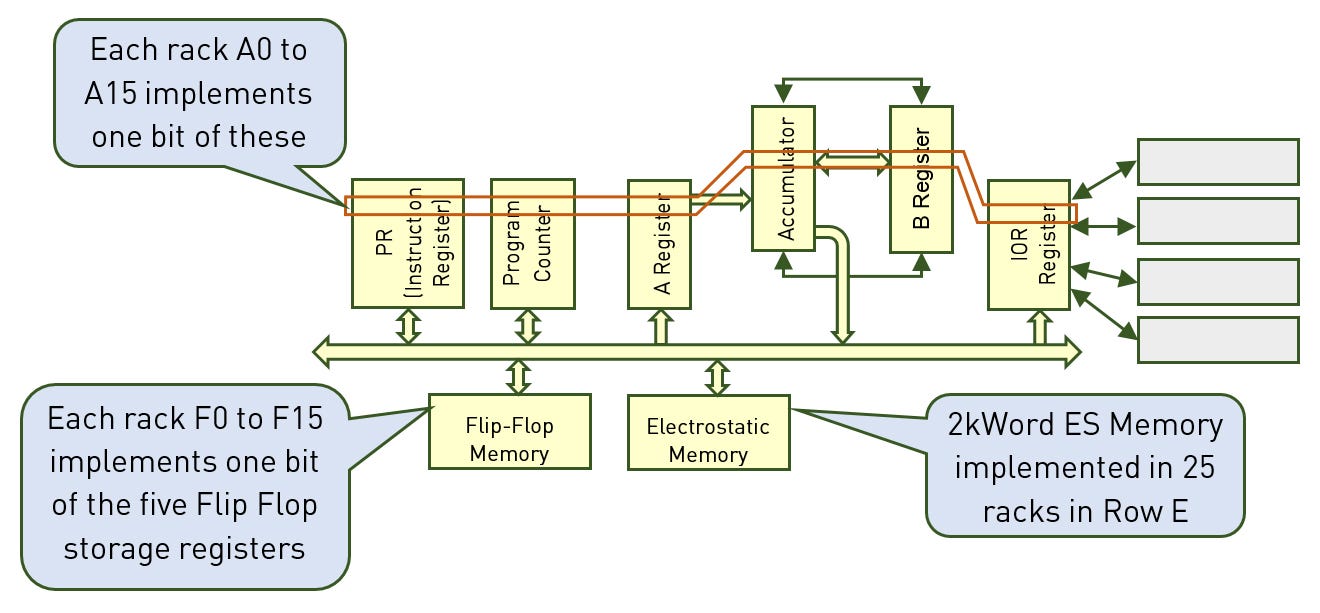
    ENIAC is often credited for being "the first calculator" but "real computers"  emerged very soon afterwards, following the famous "Von Neumann report". Today, I just found details about the WhirlWind : https://medium.com/chmcore/the-whirlwind-computer-at-chm-dab505bc52a6  and the structure is "very interesting" !

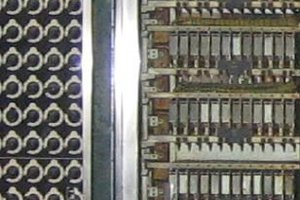
    This means that the "bitslice" organisation can be traced back to the late 1940s, because each of the 16 racks would implement one bit of the datapath, gathering one bit from each register and the ALU. There are now many, many diagrams in this report : www.bitsavers.org/pdf/mit/whirlwind/R-series/R-127_Whirlwind_I_Computer_Block_Diagrams_Volume_2_Sep47.pdf It "feels" particularly modern and reads easily, using pretty standard conventions and using very well known structures.

  • ARM1 layout

    Yann Guidon / YGDES05/25/2018 at 04:58 0 comments

    The co-creator of the first ARM processor explains the layout of the chip.

    The "datapath" uses 3/5th at the "bottom" and it looks a lot like what I have also concluded in this project. The ALU (left) is right next to the register file, in a regular, bitslice fashion. 32 slices are stacked vertically (bit0 at the bottom). A barrel shifter is placed at the right of the ALU. This is pretty similar to what I intend to do, so I reinvented the wheel again :-D

  • Front panel...

    Yann Guidon / YGDES12/22/2017 at 00:41 4 comments

    I just found that picture on eBay, for an IBM S/34 front panel :

    I have no idea what a S/34 is, BTW. Maybe a 16-bits machine ? Oh, I should have looked it up first... at http://www.corestore.org/34.htm

    However I see that they use hexadecimal rotary buttons, just like the assembler board of #YGREC and that's pretty interesting ! However, is there no disassembly board ?

  • Enabling discovery

    Yann Guidon / YGDES05/28/2017 at 23:20 2 comments

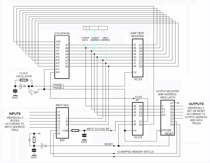
    Today, I followed @BigEd's link to his forum where he describes minimalistic systems with one page.

    There, I find a description of Dr Jefyll's One Bit ComputerOne Bit Computer

    It's indeed reminiscent of Motorola

    MC14500 1-bit computers but with no special-purpose chip. All the intelligence is in the EPROM. I admire the ingenuity of this design !

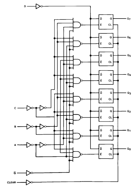
    What caught my eyes though is the output register : "4099 addressable latch" that gets 3 address bits, a latch enable and a data input.

    Wait.

    Isn't this what I complained that I couldn't find in integrated circuits ?

    I have been repeatedly suggested to make a TTL/CMOS version of AMBAP/YGREC but the big roadblock is the register set : all the registers I know are 8 bits with common clock (274, 573, 574 etc.) so a pure bitslice implementation is hard.

    Finding a 1-bit wide 8-addresses SRAM chip changes everything and the 4099 maps directly to the address decoder and latches of the register set. Add a few MUX and you're done.

    The 4099 however is a bit of an old relic. A lookup on Wikipedia finds however the 74259 : "8-bit addressable latch"

    Right : a latch, not a FF/register, just like YGREC is intended to be: a buffer latches the result during a previous clock phase to prevent a direct feedback.

    The clear input is welcome but not required. It's precious however for applications as IO port extender, which I'll also consider.

    So I just ordered a bunch of these chips and a CMOS YGREC is lurking on the horizon...

    Thanks BigEd !


    20170510:

    I got convinced into creating #YGRECmos :-)

    See the rest there !

  • There is another system

    Yann Guidon / YGDES03/23/2017 at 20:45 5 comments

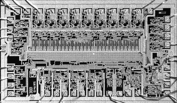
    @DL101 tells me about the Intel 3002 :

    http://www.cpu-world.com/CPUs/3002/

    This rings a bell, with the following differences :

    • only one bit per slice for the AMBAP
    • memory is linked directly to each of AMBAP's slices
    • AMBAP has only 8 or 16 registers (not 11)

    I need to find more documentation about this chip now... The die shot is glorious :

    Thanks DL !

  • Tree balancing for IC

    Yann Guidon / YGDES03/07/2017 at 14:38 0 comments

    The previously described method for balancing a tree of MUX relays has reminded me the difficulty of creating a similar dual-MUX tree in FPGA where there is no memory blocks. I encountered this problem while designing the YASEP in VHDL for Actel's A3P family and the buffering was pretty complicated.

    In ASIC/FPGA though the partition constraints are relaxed and slight unbalances can help the place/router put gates further or closer. Furthermore, the synchronicity of the arrival of all the signals ensures a more consistent timing. The elimitation of huge final fanout also brings a better overall operating speed.


    20170317

    The previous research dealt with the relay version of the register set and memory decoder, which I now realize are specific cases of the Knapsack problem. I'm now diving in the realm of Combinatorial optimization!

    With ASIC or FPGA, we can relax some of the constraints and a little imbalance (10% or less) is not critical. We don't even have a constraint of having a power-of-two number of sinks because the gate inputs are not in series and tied in the middle. As a consequence, for an ASIC or FPGA, the original approach of rotation is easy and makes sense !

    Let's examine the example of a 16-addresses register set, such as used by the #YASEP Yet Another Small Embedded Processor or the #F-CPU (v2). There are 4 address lines, and let's consider a 16-bits wide register (wider registers are just duplicates). The total fan-in is 16+32+64+128=240 for the 16×MUX16. The problematic fan-in of 128 (the last stage of the MUX) is reduced to four fan-ins of 240/4=60. This is slightlty faster (because there are less buffers to traverse, I estimate the gain to be equivalent to 1 gate propagation time due to the propagation in forward and reverse directions) and makes a more regular structure.

    Actually the structure can be decomposed in groups of bits that are as wide as the number of address lines. For our 4-addresses register set, we can create groups of 4 bits, each with a fan-in of (1+2+4+8)=15 (per bit). For a full-custom design, these nibbles can be hand-optimised then duplicated as required, but it's also possible to just let the synthesizer&place&route decide how to allocate the 4 buffer lines. I should write some VHDL for this...


    20170320

    Interleaving.

    There is more than a way to interleave the control lines. For example, simple rotations have at least 3 versions:

        step=4    step=2    step=1
    0   a b c d   a b c d   a b c d
    1   a b c d   a b c d   b c d a
    2   a b c d   b c d a   c d a b
    3   a b c d   b c d a   d a b c
    4   b c d a   c d a b   a b c d
    5   b c d a   c d a b   b c d a
    6   b c d a   d a b c   c d a b
    7   b c d a   d a b c   d a b c
    8   c d a b   a b c d   a b c d
    9   c d a b   a b c d   b c d a
    A   c d a b   b c d a   c d a b
    B   c d a b   b c d a   d a b c
    C   d a b c   c d a b   a b c d
    D   d a b c   c d a b   b c d a
    E   d a b c   d a b c   c d a b
    F   d a b c   d a b c   d a b c
    I don't even mention the direction (negative steps) or miroring (dcba instead of abcd).

    Then there is the matter of "reversal" (using a different symmetry)...

    0    a b c d
    1    b c d a
    2    c d a b
    3    d a b c
    4    d a b c
    5    c d a b
    6    b c d a
    7    a b c d
    8    a b c d
    9    b c d a
    A    c d a b
    B    d a b c
    C    d a b c
    D    c d a b
    E    b c d a
    F    a b c d
    
    All these combinations should be tried and tested to see which yields the best speed, considering that each FPGA or gate array has their own characteristics, fanout trees, etc.

    .

  • Backplane routing considerations

    Yann Guidon / YGDES01/22/2017 at 20:14 0 comments

    Edit 20170402: This entry is now moot/obsolete because of the approach explained in More balanced trees !
    However this log is a very very interesting discussion that can be useful for other similar cases.


    The last log How to balance a fanout tree has shown that it is possible to organise the coils in such a way that they are wired in strings on each (identical) bitslice board.

    This greatly reduces the complexity of the boards and the number of signals on the backplane connector. OTOH this shuffles the bits all over the place and the backplane must reorder everything.

    I have decided to implement parity checks over the DRAM read/write, as well as the register read/writes. There are 16+1=17 identical boards, parity is calculated on the 16 data boards and stored on the 17th board, using the bypass signals.

    As a consequence, there are several "shuffled busses":

    • 3 address bits for the write register
    • 3 address bits for the read/I register
    • 3 address bits for the read/R register
    • 4 address bits for the memory line
    • 5 address bits for the memory columns

    (the columns are still not well defined, but must be considered and studied)

    The "balanced shuffling" has been designed for 3 and 4 lines and 16 bits. However now it's 17 bits and the 5-bits shuffling is a new challenge...


    Let's start with the 3×16 balanced shuffle.

    There are:

    • 4 strings of blue
    • 5 strings of green
    • 5 strings of red

    Then there are 3 strings of 1, 2 and 4 coils to add at the end.

    But I have not yet studied the fanout of a CCPBRL gate to several 12V, 8-coils strings. So how many parallel strings can one relay drive ?

    Another "EMI reduction measure" is to switch approximately one half of the coils to 12V, the other half to 24V, thus reducing the draw on the power rails and halving the decoupling capacitance.


    20170320

    The above routing works for 3 and 4 control lines with 16 bits, but more bits are needed and 5 control lines might become impossible to route.

    17 is a prime number and does not look easy to use/partition. However the next number 18 is 2×3×3 and is great for use with "rotations" partitions. The would be one resistor per bit but that's a theoretical limit (I checked the numbers) and that's not a huge loss, the layout will be a bit less complicated.

    Here are two possible routings for one half (9 bits) of the slices:

    However 4 and 5 are not easy to partition with 18 bits but there is a bit of hope. A recent log "CC-PBRL : Magnetic hysteresis and fanout" has shown that strings can be 4 or 6 coils long as well.

    There is another interesting thing ! Past the 3 address bits, the other lines (with 8 and 16 fanins) "behave" differently because they are integer multiples of the required string length. The partition procedure can use more heuristics and various steps to reach the required balance. For example, we can start from the address line with the highest fanin then refine...

    However the numbers start to look unfavorable.

    • 4 address bits: 1+2+4+8=15 fanin per bitslice, 15×18=270 fanin total, or 67.5 fanin per bit, or 8.43 strings of 8 coils per address bit
    • 5 address bits: 1+2+4+8+16=31 fanin per bitslice, 31×18=558 fanin total, or 111.6 fanin per bit, or 14 strings of 8 coils per address bit

    The memory decoder is going to be a MAJOR fanout problem...


    20170324

    Let's apply some basic logic.

    It is possible to get a number that is a multiple of 3, 4 and 5 by simply multiplying them all together.

    3×4×5=60 : this is not a convenient number !

    3×5 = 15 : that's too low, even though making a 14-bits computer is not impossible (though slightly unpractical)

    17 is prime, forget it.

    18 is nice but not a multiple of 5.

    How is it possible to dump this dependency on this number 5 ?

    The next number is 6, which aligns neatly with 2×3 and its multiples (18...)

    This number 5 comes from the 32 relays, or the 16 pairs, that steer current at the columns of the DRAM arrays. The array is a 16×16 capacitors memory, creating a 256-words addressing space. Going from 32 to 64 relays increases...

    Read more »

  • How to balance a fanout tree

    Yann Guidon / YGDES12/16/2016 at 04:16 0 comments

    I have a problem since the beginning. At least for the relay version, and probably others, the register set uses two MUX8 and one DeMUX8 per bit. This creates a fanout of 1 for the LSB of the address, but a fanout of 4 for the MSB (or vice versa). There is a very significant imbalance and the LSB drives 16 relays, while the MSB drives 64 relays !

    The consequence is the increase in latency for reading operands (write decoding can overlap the execution). The LSB level can be switched quickly (FO=16) but the MSB level requires amplification stages, which delay the signal.

    Ideally each address bit should drive one third of the MUX2. The numbers have decided otherwise : 16+32+64=112 (=16×7), there is no 3 as factor and 112/3=37.333... That's very inconvenient. But I have found that it's possible to approximate this goal with the help of some bit shuffling.

    Let's remember two of the design constraints (at least for the relays) : all the bitslice are identical and a whole MUX level can't be split (on each board, or else this increases the routing complexity). As a consequence, an address bit has a "fan-in" of 1, 2 or 4. The trick is to send the 3 control signals to (globally) equal amounts of fan-in.

    This means that each address bit will drive the MUX2 stage, the MUX4 stage and the MUX8 stage equally, or in other words : each bitslice receives a rotation of the address vector.

        MUX2 MUX4 MUX8
     0   0    1    2
     1   1    2    0
     2   2    0    1
     3   0    1    2
     4   1    2    0
     5   2    0    1
     6   0    1    2
     7   1    2    0
     8   2    0    1
     9   0    1    2
    10   1    2    0
    11   2    0    1
    12   0    1    2
    13   1    2    0
    14   2    0    1
    15   0    1    2

    There is obviously a problem with the last line, because 16 has no common divisor with 3.

    Another problem is specific to the relay implementation, using the CC-PBRL method: each "high voltage string" has 8 relays, two groups of four with the signal injection in the middle. This constrains the design even more but it almost matches with the current situation.

    A "high voltage string" can drive one FI4, one FI2 and one FI1, this amounts to 7 relays. The 8th relay can be simulated by a resistor and bitslices become naturally grouped by 3 :

                M2 M4 M8
    bitslice%0   a  b  c
    bitslice%1   b  c  a
    bitslice%2   c  a  b
    
    a = b = c = 1 + 2 + 4 = 7 fan-in
    This regular pattern helps design the drive logic and estimate the complexity.

    There would be 5 identical blocks of 3 slices, plus the last part. This requires a buffer with fanout of 5+1=6 (which can be done with a high-voltage string of 8). Since there is an identical buffer for every level, the latency is identical and all the bits arrive at the same time.

    Yet this does not satisfy me because a string must have 8 relays, not 7. If the last relay is replaced with a resistor, 1/8th of the power gets wasted and this is not insignificant...

    I found a much better circuit, which is explained with the simple diagram below:

    Each group of 4 bitslices (wich evenly divides 16) has the same organisation (they can be mirored for convenience). Each bitslice has exactly one occurence of each color.

    There are three full "long strings" of 8 Fan-In:

    • 4-4
    • 2-2-4
    • 1-1-2-4

    All these long strings have a "middle point" where the signal can be injected.

    The remaining strings (1-1 and 2) can be assembled into a long string each, and it is just perfect (2-2-2-2 and 1-1-1-1-1-1-1-1) both in length and halvability.

    Conclusion : the balance is not perfect but still quite good:

    • 4 strings of blue
    • 5 strings of green
    • 5 strings of red

    It's certainly a bit more complicated than the initial fanout tree but no power is wasted in resistors. The fanout of 4 can be handled by 2 low-voltage CCPBRL (4 relays). I'll have to see if the CCPBRL can handle a fanout of 3, so the case of 5 can be handled with 2 and half low-level CCPBRL (5 relays and a resistor).

    Finally, the layout of the bitslices is not changed : the coils of each level are wired in series (on each board) and the connector does not need to provide direct access to each and every relay with a pair of wires. This keeps the design compact.

    The only requirement is to use the same...

    Read more »

  • Project split

    Yann Guidon / YGDES12/04/2016 at 00:00 0 comments

    This project was meant to be an exploration of a design space and examination of a ruleset, not about a specific implementation.

    I decided to split the project and continue the relay implementation as #YGREC16 - YG's 16bits Relay Electric Computer while I discuss here about higher-level considerations and features which will be common to other designs (such as #F-CPU and #YASEP Yet Another Small Embedded Processor )

  • DRAM boards

    Yann Guidon / YGDES12/01/2016 at 19:48 0 comments

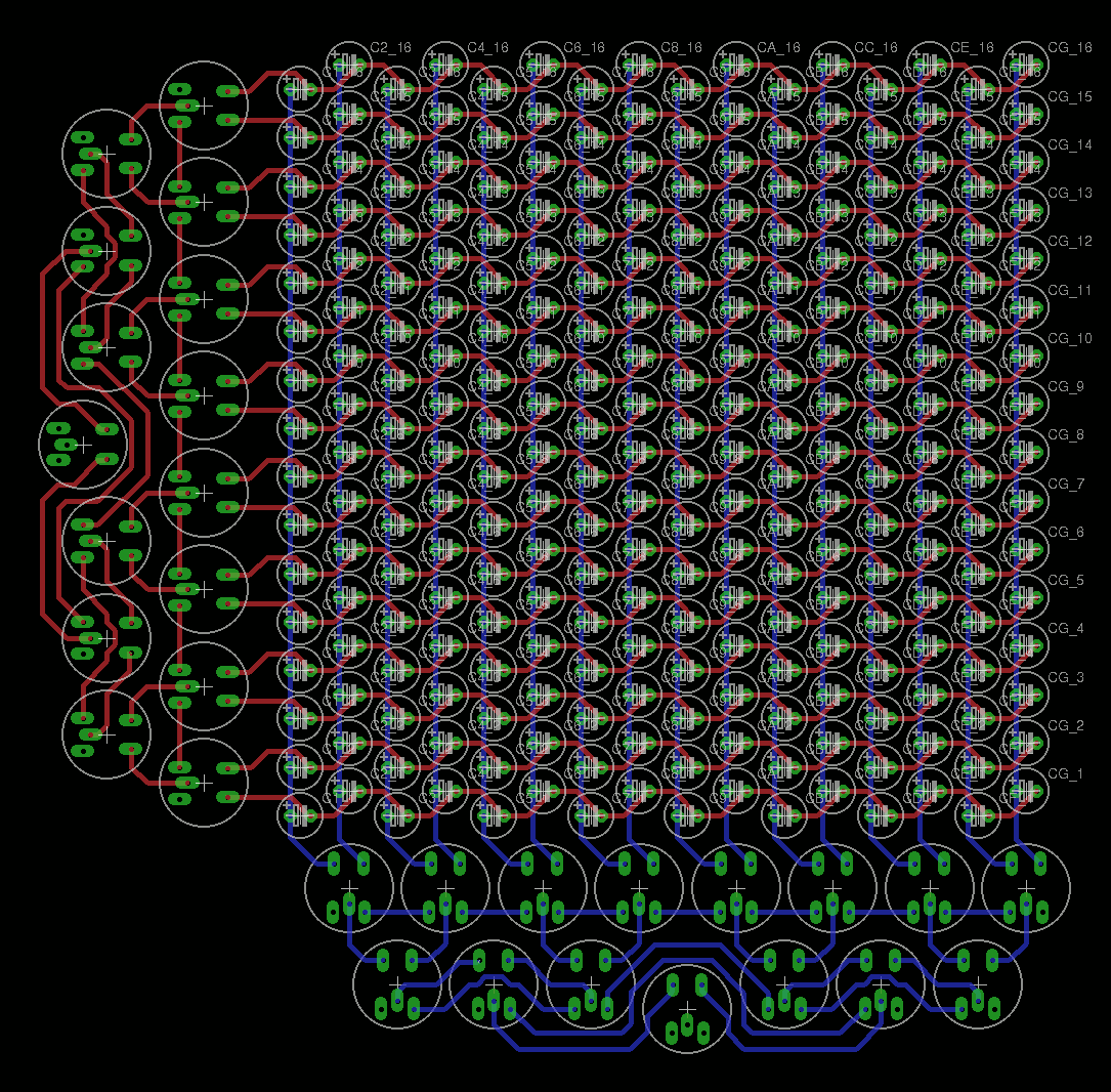
    I have settled with a 16×16 capacitor array module, which I routed (with great pain) with Eagle:

    With such a module, the design is more flexible so I can implement as much RAM as I need or want. I can swap modules if one is found defective. I can build as many bitplanes as required, for example for the 17th bit for parity.

    The above layout uses 6mm diameter capacitor, though I also have 5mm in stock, at least only one board model is manufactured.

    For the driving circuits, the best I could come up is a 256-words array. Each bitplane needs their set of relays (I tried otherwise and failed, or else I'd need tons of diodes and stuff, which makes the system more complex and probably delicate).

    Each bitplane then has 15 relays for the X MUX16 and 15 for the Y DeMUX16. Plus the grounding relay, that's 31 relays per bitplane. With 17 bitplanes, that's 527 relays for 256 words... and 2.7A @12V=32W for the static power consumption.


    Pretty simple, right ?

View all 38 project logs

Enjoy this project?

Share

Discussions

zpekic wrote 06/16/2020 at 06:43 point

Very interesting project - I have a similar one in early stages in my papers, it was to be a 1-bit slice using GAL22V10. 8 internal registers feeding through 2 parallel 8-to-1 MUXs into a 8 operation ALU (which is a 8-to-1 MUX, some selections implement left and right shift, and pass through of external data inputs). Write back to "regs" is implemented as a 2-to-1 MUX in front of the D input. Select of these is connected to to a 3-to-8 decoder with enable. This way in one cycle 2 independent values can be read and written into third (3 address architecture)

  Are you sure? yes | no

Squonk42 wrote 03/31/2017 at 20:07 point

And for right shift, just add a 2:1 MUX at the output. You can combine it with the last XOR into a bigger MUX to lower the propagation delay.

  Are you sure? yes | no

Yann Guidon / YGDES wrote 03/31/2017 at 20:25 point

That's an idea, if only the technology is only MUX-based.

Anyway I want the MUX before the ALU...

Among others, it saves a lot of processing for the #Game of Life bit-parallel algorithm

  Are you sure? yes | no

roelh wrote 12/02/2016 at 19:52 point

Hi Yann,

just saw your new  DRAM board.....I think it will not work, you really need diodes as in the TIM8 of Rory Mangles. 

  Are you sure? yes | no

Yann Guidon / YGDES wrote 12/03/2016 at 17:48 point

Hi !

Thank for the comment.

Actually, in the chosen configuration, I don't need diodes.

I couldn't figure why the diodes were needed in the TIM8. The diagram is not clear enough.

In the chosen case with only 16×16 bits per plane, there is no need of diodes because each capacitor is connected only as needed. The + side is connected to the sense, the - to 0V. Only one capacitor at a time. The capacitors are not connected directly or indirectly to other capacitors, unless the enable strobe is asserted.

Diodes are required if the demux is shared with all the bitplanes. This saves maybe 1/2 of the relays but there are disadvantages too:

* triple the parts count, triple the parts to solder ! Diodes are cheap but become a significant effort to solder. 1KW means 17K capacitors and 34K diodes ! I don't have a pick&place machine...

* The diode system I came up with, uses 2× relays per selected line instead of 1 so the capacity must be higher to be worth the efforts.

* diodes leak. not much but this can make a significant difference, like from 2 minutes to 1 minute of safe retention. Diodes have a little capacitance too, which can act as a tiny divider when combined to another capacitor. After a thousand spikes, this might erode the data and decrease reliability.

* This increased leak also increases the requirement of the refresh but as the memory size increases, the refresh can't scan every cell fast enough. For example, if I can manage to build 1Kwords, with 1 minute of retention, the refresh goes to 1024/60=17 addresses/second, which saturates the data bus and hogs the processor. Remember, I try to reach about 20 IPS...

In the end, separate decoders simplify this. The system draws more power and costs more in relays but

* I don't need huge amounts of RAM. Just enough to explain basic computer constructs such as variables, loops, stacks, arrays...

* 256 words is still larger than #The T-1: A discrete 8-bit Stack Computer :-D

* There is no current path from/to the capacitors unless explicitly accessed so the retention is longer and the refresh is sporadic in the background

* Less parts to solder. I'll use classic PCB fabs but I'll assemble the boards myself...

I'll still examine other configurations... My MUX approach might not be the best one, for example.

  Are you sure? yes | no

roelh wrote 12/03/2016 at 20:00 point

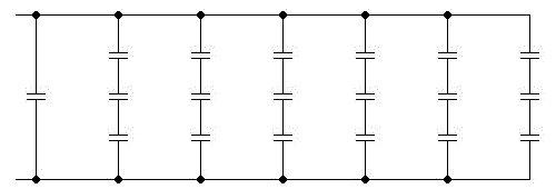
When you select a single capacitor, all other capcitors will also be selected for 1/3. The following diagram is just another way of drawing your circuit. The selected capacitor is the leftmost one. 


So if you charge the intended capacitor, all other capacitors will also receive some charge. Same for discharging. So after writing your bits to a few capacitors, the charge in all other capacitors will have changed to such an amount that the original information is not readable any more....

The diodes will isolate the capacitors from each other, in that case the other capacitors are not affected when you charge or discharge a certain one.

  Are you sure? yes | no

Ted Yapo wrote 12/03/2016 at 20:05 point

Actually, I think the schematic above solves the loop issue for the 2x2 matrix case, but doesn't work for larger arrays.  There aren't any loops with 4 neighboring capacitors, which is neat, but if you look at larger loops, they're still a problem.

  Are you sure? yes | no

Yann Guidon / YGDES wrote 12/03/2016 at 20:15 point

Thank you guys, I start to "see" what you mean...

  Are you sure? yes | no

Yann Guidon / YGDES wrote 12/03/2016 at 20:19 point

Now I wonder what the solution might be :-/

  Are you sure? yes | no

Yann Guidon / YGDES wrote 12/03/2016 at 21:05 point

Let's discuss about this on #YGREC16 - YG's 16bits Relay Electronic Computer because I'm moving all the technical/implementation stuff there :-)

  Are you sure? yes | no

roelh wrote 09/13/2016 at 20:39 point

Hi Yann,

here is my TTL fast-carry circuit:

[ edit: picture was deleted by Hackaday. Find it here:

  https://hackaday.io/project/160506-4-bit-ttl-alu/log/151032-the-fast-carry-circuit  ]

The first diagram is the classic carry circuit, that has a P (propagate), G (Generate)  and Cin as inputs.

The second diagram is the stepstone to the fast carry. The carry generation can be done by a multiplexer. The G signal can now simply be connected to the A (or B) input signal, and the name "G" is actually not appropriate for this signal....

In the third diagram, the multiplexers of three adjacent bits are combined into a single 74HC151 8-input multiplexer. So for 3 adjacent bits, the Cin has to pass only a single IC before arriving at Cout. Note that the 151 has an enable input, that can be used to disable the carry for the logic functions of the ALU.

Now the circuit for transistor logic follows, especially interesting if you want to minimize the number of transistors. Could also be used for DVTL ( Diode-Vacuum-Tube-Logic).

[ edit: Hackaday removed the picture. Find it here:

https://hackaday.io/project/160177-alu-in-dctl-technology/log/151068-or-use-a-lot-of-diodes-and-a-few-transistors  ]

The top part calculates the (inverted) carry. The lower part calculates the (inverted) sum, with the function   SUM =  (  ( A or B or Cin )  and /Cout  )  or  ( A and B and Cin )

With a few extra parts, the carry could be forced to always be active or inactive. In that case the circuit will perform a simple AND (for carry active, /Cout=low)  or an OR (for carry not active, /Cout=high).

To connect the /Cout to Cin of the following bit, you will need an extra transistor inverter, or you could use inverted logic for every alternate bit.

The make this into a working ALU, resistor values must be calculated and some parts must be added for optimal circuit response. It is supposed that the inputs can sink current but als source current (for the OR gate).

BTW your relay computer tends to become just as complex as mine...  

  Are you sure? yes | no

Yann Guidon / YGDES wrote 09/13/2016 at 20:52 point

Hey, thanks a lot ! this is very interesting :-)

I'll skip the fast-carry for now, because the thing is already quite complex, as you noticed ;-) But I'm seeing which method is most convenient if I want to speed up my device.

BTW I haven't seen any update recently for #RISC Relay CPU... Any progress on the physical side ?

  Are you sure? yes | no

roelh wrote 09/14/2016 at 17:48 point

Hi Yann

Expect an update of the RRC soon. I again changed the instruction set and the assembler/simulator accordingly. Also thought about SIN/COS calculation, CORDIC will not be used because it is only efficient for binary, not for BCD calculations. Using a short table combined with Taylor expansion will do the job with approx. 5 multiplications and several additions. I still don't know how to do square root, using logarithmics is easy to do but perhaps not very accurate, there must be a better way, I'm open to suggestions. On the HW side, I decided how to divide everything over several pcb's ( 6 different ones ). I designed 2 pcb's and the 3rd one is half done. I'll use a relay with 1 msec switching time, that will give the calculator its speed....

  Are you sure? yes | no

Yann Guidon / YGDES wrote 09/15/2016 at 02:41 point

For SQRT(), use the Newton-Raphson method :-)

  Are you sure? yes | no

roelh wrote 09/11/2016 at 13:24 point

Hi Yann,

I did spend a lot of time finding optimal ALU solutions.

The best I could find (for TTL) was this:

[ edit: picture was deleted by hackaday, find it here: https://cdn.hackaday.io/images/2724861697734563209.png ]

The key to the schematic is, that a single multiplexer (the lower one), can generate every possible logic function of two variables. (Only the the most useful ones are in the table).

For logic functions, all orange carry wires should be "0" (The grey CARRY ENABLE signal must be low to accomplish this for the carry output, the connection of the grey wire to the multiplexer is not very obvious, the multiplexer symbol that I used in the drawing did not have an ENABLE input). The output of the ALU is equal to the logic output (on the red wire).

For addition, the upper multiplexer part will generate the "majority" function of the 3 inputs, giving the new carry at its output. The incoming carry is exor'ed to the logic output (logic function should be set to XOR for adition). 

The ALU can also pass one of the input signals unmodified, so it can be used for a LOAD instruction to get immediate or memory data into one of the registers. For the control section, the LOAD is just another arithmetic instruction, this simplifies the control section of your CPU.

With the addition of a 74HC151, it is possible to do a fast-carry that calculates a carry for three levels at once.

The above schematic can easily be adapted to relay or other technologies.

For a relay based ALU, see the file "relay CPU technology V1.7" in the files section of https://hackaday.io/project/11012-risc-relay-cpu, that is base on the same idea. The logic function is performed in diode-resistor logic, combined with relay logic.

For a diode-transistor based version, there is another solution that needs only a few transistors. If you're interested I will make a drawing.

  Are you sure? yes | no

Yann Guidon / YGDES wrote 09/11/2016 at 13:30 point

Of course I'm interested :-)

Thanks for the explanations !

(and I already follow the #RISC Relay CPU :-) )

  Are you sure? yes | no

Yann Guidon / YGDES wrote 09/11/2016 at 13:41 point

Oh now I recognise the MUX trick for arbitrary logic functions, I used it 15 years ago in the #F-CPU's ROP2 unit ^_^

Now, I see something is missing : shift left/right.

  Are you sure? yes | no

Squonk42 wrote 03/31/2017 at 20:03 point

For shift left, it's easy: just set A=B

  Are you sure? yes | no

Yann Guidon / YGDES wrote 03/31/2017 at 20:08 point

Michel : that's not enough, because often indices need to be shifted to compute a word-aligned address with offset :-)

  Are you sure? yes | no

Similar Projects

Does this project spark your interest?

Become a member to follow this project and never miss any updates