-
1MB+ SRAM Build
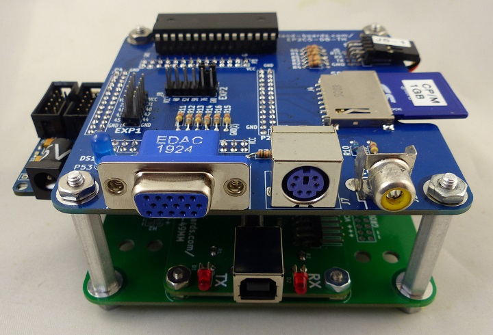
06/01/2021 at 13:34 • 0 commentsDid a build for the RETRO-EP4CE15 card. The build uses the 1MB of external SRAM as 64 banks of 16KB each. The banks are in the CPU address range of 0xC000-0xDFFF. There is a bank control register which initializes to bank=0 at power up or reset.
The 6800 CPU has a total of 60KB SRAM 9addressable. The rest of the RAM is internal to the EP4CE15 FPGA. The CPU memory map is:
--    Memory Map
--        x0000-x7fff - 32KB Internal SRAM
--        x8000-xbfff - 16Kb SRAM bank (64 banks)
--        xc000-xefff - 12KB Internal SRAM
--        xf000-xffff - 4 KB ROM (minus I/O space)
--        xfc00-xfcff - I/O space
--            xfc18-xfc19 - VDU/UART (6850 Interface)
--            xfc28-xfc29 - UART.VDU (6850 Interface)
--            xfc30 - Bank Select register (r/w)
The 12KB of SRAM could be initialized at boot and could function as a ROM space for an O/S, etc.
-
Made explicitly named 60KB ROM file
06/01/2021 at 13:30 • 0 commentsMade a MIKBUG ROM that is explicitly named (DGG_MIKBUG_60KB.xxx) to distinguish it from the 32KB "original* version.
It uses I/O in the 0xFCxx range.
-
32KB MIKBUG
05/31/2021 at 14:05 • 0 commentsCreated a 32KB MIKBUG which allows the design to work with the Internal SRAM on the EP4CE15.
Uses the original $80xx addresses for the VDU/ACIA.
GitHub repo is here. The hex file name is: DGG_MIKBUG_32KB.hex.
-
60KB of SRAM
06/29/2020 at 11:03 • 0 commentsEarlier we moved MIKBUG to $F000-$FFFF. We also opened a window for I/O from $FC00-$FCFF.
The entire space from $0000-$EFFF can be now used for SRAM.
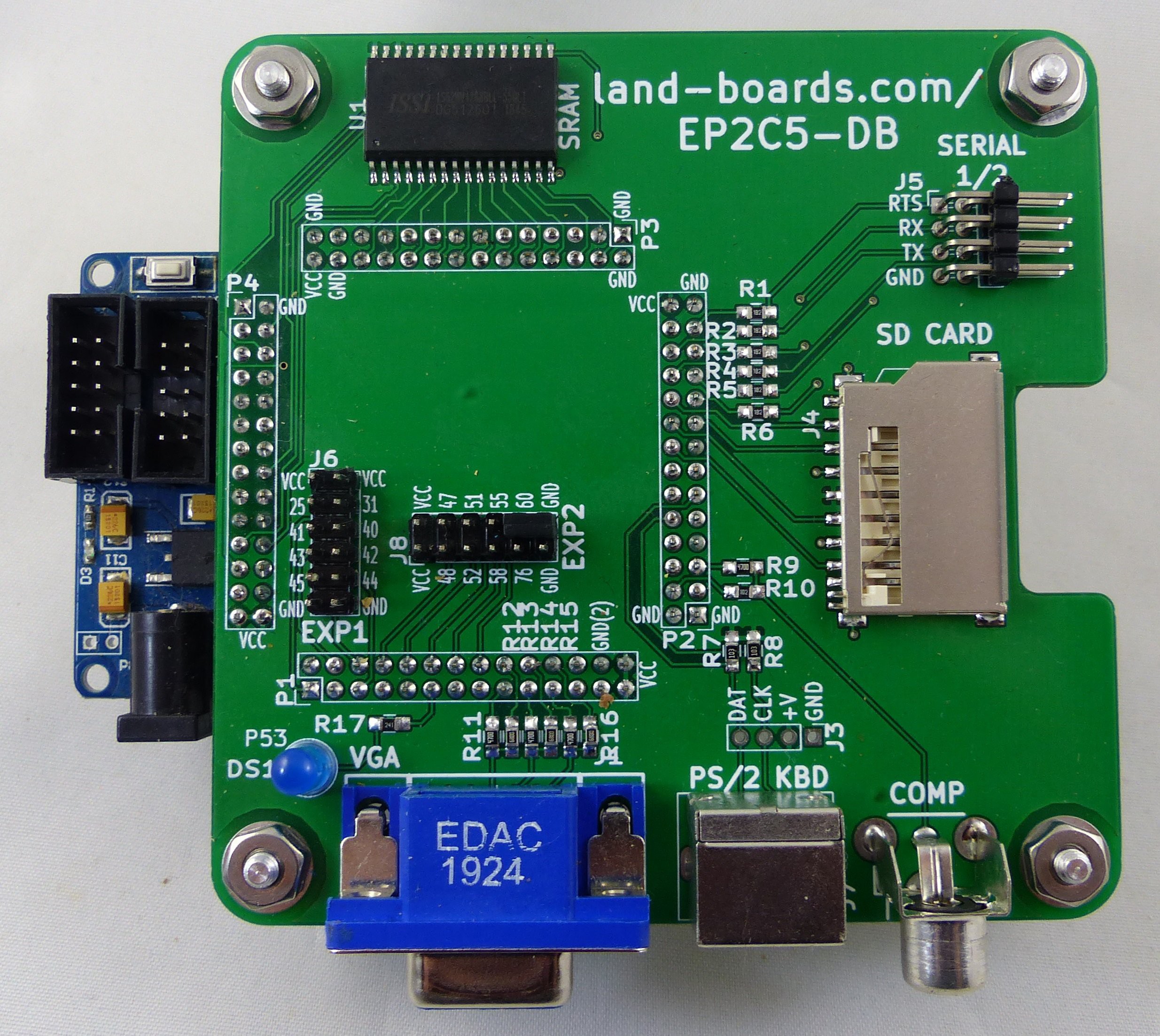
Works well on EP2C5-DB card.
![]()
-
Loading Test Program
06/29/2020 at 10:18 • 0 commentsWrote a small test program to get a character from the serial port and write it back to the serial port. Uses the MIKBUG serial in and out routines.
; TESTCODE.ASM
; DOS command line to assemble source
;     a68 TESTCODE.ASM -l TESTCODE.LST -s TESTCODE.s
; & to download S-record to card
; Copy/paste into PuTTY terminal

ACIACS	EQU	$FC18
ACIADA	EQU	$FC19

START
			ORG	$0000
LBACK
		BSR		GETCHAR
		BSR		OUTPUTA
		JMP		LBACK
;
GETCHAR	PSHB
WAITIN	LDAB	ACIACS	; LOAD ACIA CONTROL REGISTER
	ASRB	        ; SHIFT RIGHT  ACIADA
	BCC 	WAITIN	; IF CARRY NOT SET THEN AGAIN
	LDAA 	ACIADA	; LOAD DATA REGISTER
	PULB		; RESTORE B REGISTER
	RTS
;
OUTPUTA	PSHB		; SAVE B
WAITOUT	LDAB	ACIACS	; LOAD ACIA CONTROL REGISTER
	ASRB		; SHIFT RIGHT
	ASRB		; SHIFT RIGHT
	BCC 	WAITOUT	; IF CARRY NOT SET DO AGAIN
	STAA 	ACIADA	; SEND CHARACTOR TO ACIA
	PULB		; RESTORE B
	RTS		; RETURN FROM ROUTINE

	END
Assembles to:
                        ; TESTCODE.ASM
                        ; DOS command line to assemble source
                        ;     a68 TESTCODE.ASM -l TESTCODE.LST -s TESTCODE.s
                        ; & to download S-record to card
                        ; Copy/paste into PuTTY terminal

   fc18                 ACIACS	EQU	$FC18
   fc19                 ACIADA	EQU	$FC19
                        ;
   0000                 START
   0000                 			ORG	$0000
   0000                 LBACK
   0000   8d 05         	BSR		GETCHAR
   0002   8d 0f         	BSR		OUTPUTA
   0004   7e 00 00      	JMP		LBACK
                        ;
   0007   37            GETCHAR	PSHB
   0008   f6 fc 18      WAITIN	LDAB	ACIACS	; LOAD ACIA CONTROL REGISTER
   000b   57            	ASRB	        ; SHIFT RIGHT  ACIADA
   000c   24 fa         	BCC 	WAITIN	; IF CARRY NOT SET THEN AGAIN
   000e   b6 fc 19      	LDAA 	ACIADA	; LOAD DATA REGISTER
   0011   33            	PULB		; RESTORE B REGISTER
   0012   39            	RTS
                        ;
   0013   37            OUTPUTA	PSHB		; SAVE B
   0014   f6 fc 18      WAITOUT	LDAB	ACIACS	; LOAD ACIA CONTROL REGISTER
   0017   57            	ASRB		; SHIFT RIGHT
   0018   57            	ASRB		; SHIFT RIGHT
   0019   24 f9         	BCC 	WAITOUT	; IF CARRY NOT SET DO AGAIN
   001b   b7 fc 19      	STAA 	ACIADA	; SEND CHARACTOR TO ACIA
   001e   33            	PULB		; RESTORE B
   001f   39            	RTS		; RETURN FROM ROUTINE

   0020                 	END
fc18  ACIACS        fc19  ACIADA        0007  GETCHAR       0000  LBACK
0013  OUTPUTA       0000  START         0008  WAITIN        0014  WAITOUT
S-Record file:
S11300008D058D0F7E000037F6FC185724FAB6FCD8
S113001019333937F6FC18575724F9B7FC19333913
S9030020DC
Downloaded to the card.
Works!
-
MIKBUG S-Record Load Dropping Characters
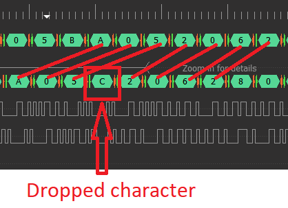
06/28/2020 at 13:30 • 0 commentsMIKBUG is dropping a character during s-record-loads. Dropped baud rate from 115,200 to 9600 and it still drops character. RTS is not being de-asserted even when changing RTS buffer assertion levels so I don't think it's an overrun. I have seen RTS deassert on larger transfers.
Trace is using DS Logic Plus on Tx, Rx, RTS_N lines.
Load works OK at 2400 baud. Strange behavior.
6800 S-Record Load Assembly Code
S1STRING    FCC    "This S1 load has entered system scratch area"
        FCB    $0D,$0A,$04
; DGG - S Record loader
SLOAD        EQU     *
        PSHA                ; Save A register
        STX    TEMPX1       ; Save X register
        ; DGG - Next line was BSR but fixing the CPX VAR lines made it too far away
GOAGAIN JSR    GETCHAR      ; Get first character from ACIA
        ;  Wait for an S
        CMPA   #$53         ; Is it "S"
        BNE    GOAGAIN      ; If not go read again
        BSR    GETCHAR      ; Get second character in frame
        CMPA   #$39         ; Is it "9"
        BEQ    RECOVER      ; If "9" go and end read
        CMPA   #$31         ; Is it a "1"
        BNE    GOAGAIN      ; If no then go start again
        CLR    TEMPA        ; Clear Frame length
        BSR    GETHEX       ; Get frame length from input stream
        SUBA   #$02         ; Subtract the checksum
        STAA   BYTESTORE    ; Save frame length
        BSR    GETADD       ; Read next two bytes for dest address
GETCOUNT BSR   GETHEX       ; Get the byte number
        DEC    BYTESTORE    ; decrement counter
        BEQ    INCOUNT      ; If zero go to increment byte count
        STAA   0,X          ; Store read byte into memory
        CMPA   0,X          ; Test if RAM OK
        BNE    QUESTION     ; If write failed send Question and abort
        INX                 ; Increment address pointer
; DGG - CPX was CMPX which did not compile and was commented out
; DGG- Changed branch from BGE to BLE (I think the compare worked the other way)
        CPX    VAR          ; Is it the system scratch area
        BLE    S1EXIT       ; Abort if close to system scratch
        BRA    GETCOUNT     ; go get another byte
;
S1EXIT  LDX    #S1STRING    ; Protect System Scratch Abort S1
        BSR    OUTSTR       ; Print abort string
        BRA    RECOVER      ; Back to console prompt
;
INCOUNT INC    TEMPA        ; Increment tempa
        BEQ    GOAGAIN      ; If zero go for another frame
QUESTION LDAA  #$3F         ; Load question mark
        JSR    OUTPUTA      ; Send to console
RECOVER LDX    TEMPX1       ; Restore "X"
        PULA                ; Restore A
        JMP    CONTRL       ; Jump to exit
;
;
GETADD  BSR    GETHEX       ; Read in byte
        STAA   ADDRESS      ; store in first part of address
        BSR    GETHEX       ; Get another byte of data
        STAA   ADDRESS1     ; store in second address register
        LDX    ADDRESS      ; Load X register both bytes of address
        RTS                 ; Return from sub routine
;
;    ADD IN THE ADDRESS OFFSET
;
GETHEX  BSR    CONVHEX  ; Go get byte of data and convert to binary
        ASLA            ; Shift the the 4 bits into msb
        ASLA            ; Shift the the 4 bits into msb
        ASLA            ; Shift the the 4 bits into msb
        ASLA            ; Shift the the 4 bits into msb
        TAB             ; Transfer "A" to "B"
        BSR    CONVHEX  ; Go get byte of data and convert to binary
        ABA             ; Add 4 bits in "A" and "B" into "B"
        TAB             ; Transfer "A" to "B"
        ADDB   TEMPA    ; Add into checksum
        STAB   TEMPA    ; Add into checksum
        RTS             ; Return from sub routine
;
CONVHEX JSR    GETCHAR  ; Get HEX character from ACIA
        SUBA   #$30     ; Convert to binary
        BMI    QUESTION ; Convert to binary
        CMPA   #$09     ; Convert to binary
        BLE    RETURN2  ; Convert to binary
        CMPA   #$11     ; Convert to binary
        BMI    INCSTACK ; Convert to binary
        CMPA   #$16     ; Convert to binary
        BGT    INCSTACK ; Convert to binary
        SUBA   #$07     ; Convert to binary
RETURN2 RTS             ; Return from sub routine
Solution
Shut off the echo using "N" command and it works even at 115,200 baud.
Type "O" to turn on after transfer.
Need to turn off echo if using built-in INEEE routine from programs you write otherwise characters will be echoed. Alternately could Set/Clear ECHO flag. Might want to save ECHO flag.
0xf1f3 INEEE
0xf20a OUTEEE
-
Maxed Out SRAM
06/26/2020 at 13:49 • 0 commentsCouldn't resist tweeking the 6800/MIKBUG files. Opened up a window of the ROM from 0xFC00-0xFCFF and relocated the I/O up to that range. Had to do more mods to the MIKBUG source file.
Now MIKBUG has a phenomenal 60KB of SRAM.
Notes when altering MIKBUG source code
Need to set the start of the 128 bytes scratchpad SRAM
VAR EQU $EF00 ; TOP OF USER MEMORY
Need to set the I/O addresses
; ACIACS EQU $FC18 ;V1 has $8000, $8001 ACIADA EQU $FC19 ; PIAD1A EQU $FC00 ;V2 has PIA support PIAS1A EQU $FC01 PIAD1B EQU $FC02 PIAS1B EQU $FC03 ; PIAD2A EQU $FC08 PIAS2A EQU $FC09 PIAD2B EQU $FC0A
Need to set the start of the codePIAS2B EQU $FC0B
; ; OPT MEMORY ; ORG $F000 ;V1 has $F800H -
Hand Jamming Code
06/25/2020 at 22:49 • 0 commentsMIKBUG provides support routines. The listing file has the addresses of the routines.
INEEE is the input routine which gets a character from the current port.
OUTEEE is the output routine which sends a character to the current port.
Port loopback code:
; INEEE    EQU    $F1F3
; OUTEEE   EQU    $F20A

LOOP4VR
    JSR    $F1F3
    JSR    $F20A
    BRA    LOOP4VR
Code assembles to:
0000 LOOP4VR
0000   bd F1 f3 JSR $F1F3
0003   bd F2 0a JSR $C20A
0006   20 f8    BRA LOOP4VR
E to change memory:
>E 0000
>0000 55 BD
>0001 55 F1
>0002 55 F3
>0003 55 BD
>0004 55 F2
>0005 55 0A
>0006 55 40
>0007 55 F8
>0008 55 <ENTER>
V to dump memory:
>V
FROM ADDR 0000
0000 BD F1 F4 BD  F2 0A 40 F8  55 55 55 55  55 55 55 55
     ......@.UUUUUUUU
Type N to turn off echo.
J to jump to program:
>J TO ADDR 0000
Type chars and they get echoed.
ITTEESSTTIINNGG TTHHIISS WWOORRKKZZ LLOOLLOOLLOOLLOOOOLL -
MIKBUG with 56K of SRAM
06/25/2020 at 19:56 • 0 commentsThe EP2C5-DB card has 128KB of SRAM external to the FPGA. I wanted to get access to more of that SRAM. There were a couple of things in the way. Getting to 32KB was easy. To get past the 32KB limit I needed to move the MIKBUG I/O up in the memory space. I also needed to move the ROM up to the top of RAM.
M6800_MIKBUG - Tested/Works
- MC6800 CPU
- Running MIKBUG from back in the day (SmithBug ACIA version)
- 12.5 MHz
- 56K (external) RAM version
- MC6850 ACIA UART
- Video Display Unit (VDU)
- Color attributes
- XGA 80x25 ANSI character display
- Extended (256) character set
- PS/2 keyboard
Memory Map
- $0000-$DFFF - 56KB external sRAM
- $0000-$DEFF - User RAM area
- $DF00-$DFFF - scratchpad used by MIKBUG
- I/O Map
- $E018-$E019 - VDU
- $E028-$E029 - ACIA
- Pin_60 of the FPGA swaps addresses of VDU and ACIA port
- Installed (Pin_60 to Ground) uses Serial port
- Removed uses VDU
- $F000-$FFFF - MIKBUG ROM
Changing MIKBUG ROM Location
I am using the a68 assembler to assemble code to a S-record file and the S-Record utilities to re-shift the address of the assembled S-Record down to the state of the ROM as well as create the HEX file needed by Quartus. The ROM monitor source code is V2_DIS_corrected.ASM.
The commands are:
a68 V2_DIS_corrected.ASM -l V2_DIS_corrected.LST -s smithbug.s
srec_cat smithbug.s -offset - -minimum-addr smithbug.s -o smithbug.hex -Intel
The output file, smithbug.hex is then copied into the Multicomp ROMs location. Next run Multicomp and select Processing then Update Memory Initialization File. If you get a warning at this point of when you build the FPGA programming file double click the end delete the highlighted (next to the last line) in the hex file and save. Re-build at that point and the error will go away.
Note than any code you have which relies on fixed locations for the MIKBUG ROM routines will need to be updated to use the new addresses. The listing file, V2_DIS_corrected.LST, contains the listing from the assembler output.
-
MIKBUG with 9KB SRAM
06/25/2020 at 13:49 • 0 commentsMade a new build of MIKBUG. It runs serial only but gives 9KB of SRAM internal to the SRAM.
![]()
M6800_MIKBUG _Serial- Tested/Works
- MC6800 CPU
- Running MIKBUG from back in the day (SmithBug ACIA version)
- 12.5 MHz
- 9K (internal) RAM version
- 8.5K User SRAM
- 0.5K Scratchpad SRAM
- MC6850 ACIA UART
- No VDU
Memory Map
- $0000-$21FF - 8.5KB SRAM (internal RAM in the EPCE15)
- User program SRAM
- $7E00-$7FFF - 512B SRAM (internal RAM in the EPCE15)
- 0x7E00-0x7EFF available for user
- 0x7F00-0x7FFF are used as scratchpad RAM by MIKBUG
- $8018-$8019 - ACIA
- $C000-$CFFF - MIKBUG ROM (repeats 4 times from 0xC000-0xFFFF)
 land-boards.com

