zpekic
-
Color bus hack
04/11/2021 at 03:05 • 0 commentsOne very interesting feature of V99X8 VDPs is the "color bus". These 8 pins usually carry the color (or color index) of the pixel being drawn, but can be also used as inputs for external video signals. These modes are described on pg. 109 of the "technical data book".
I neglected to look deeper at the color bus, but fellow hackaday user tomcircuit gave me a great idea how to use it. I already had the whole software + hardware + test rig 95% ready, here are the changes I did to use it.
1. Atrocious hardware hack
This is something that should never be done, but in this case it was the quick and lazy way - I soldered 4 wires directly to bits 3...0 of the color bus to tap into those signals (pins 16, 17, 18, 19).
![]()
this creates a 4-bit digital pixel signal. The original project had 3 digital lines (R, G, B) so I had to add 1.
VDP_I_DIG <= PMOD(4); -- INPUT! -- Bit3 from color bus2. Extending the FPGA pixel width from 3 to 4 bits
The "DLCLK" signal is not used in this project, instead I recreated it in the FPGA using CPUCLK, and this internal clock can be tweaked using a delay line configurable by switches on the FPGA board. This allows timing "fine tuning":
i_delayed <= i_line(to_integer(unsigned(switch(7 downto 6) & '1'))); -- use "red" switches
r_delayed <= r_line(to_integer(unsigned(switch(7 downto 6) & '1')));
g_delayed <= g_line(to_integer(unsigned(switch(5 downto 4) & '1')));
b_delayed <= b_line(to_integer(unsigned(switch(3 downto 2) & '1')));
The new "i" line has to be brought to the sampler to be captured. Luckily the MSB of the "color nibble" was free.
Mode Dual port RAM byte structure Notes RGB 0RGB0RGB MSB is hard coded to 0 Color bus c3c2c1c0c3c2c1c0 c3 = "i" signal
c2 = pin 17 drives "R" input
c1 = pin 18 drives "G" input
c0 = pin 19 drives "B" inputThe net result is very clean 2 16-color pixels per byte in FPGA dual port video RAM:
on_sample_pulse: process(sample_pulse, i, r, g, b, sample)
begin
if (rising_edge(sample_pulse)) then
sample <= sample(3 downto 0) & i & r & g & b;
end if;
end process;
3. Color palette update
With 3 bits per pixel directly mapped to R, G, B there is not much to be done in terms of color palette: 000 will logically map to "black" and 111 to "white" etc.
With 4 bits (or more, up to 8), the color bus can be interpreted to carry the "index" and an external memory (for example 256 * 24 bits) can define the exact color meaning of each index. This is of course easy to do in FPGA so here the mapping I implemented:
-- standard TMS9918 16-color palette (http://www.cs.columbia.edu/~sedwards/papers/TMS9918.pdf page 26)
signal video_color: color_lookup := (
    color_transparent,    -- VGA does not support is, so "black"
    color_black,
    color_medgreen,
    color_ltgreen,

    color_dkblue,
    color_ltblue,
    color_dkred,
    color_cyan,

    color_medred,
    color_ltred,
    color_dkyellow,
    color_ltyellow,

    color_dkgreen,
    color_magenta,
    color_gray,
    color_white
    );
With the palette defined above, the VDP color can be described as "any 16 colors out of 256", that's because the width of the palette register is 8 bits, defined as:
RRRGGGBB
Here is the definition of the colors used in the palette:
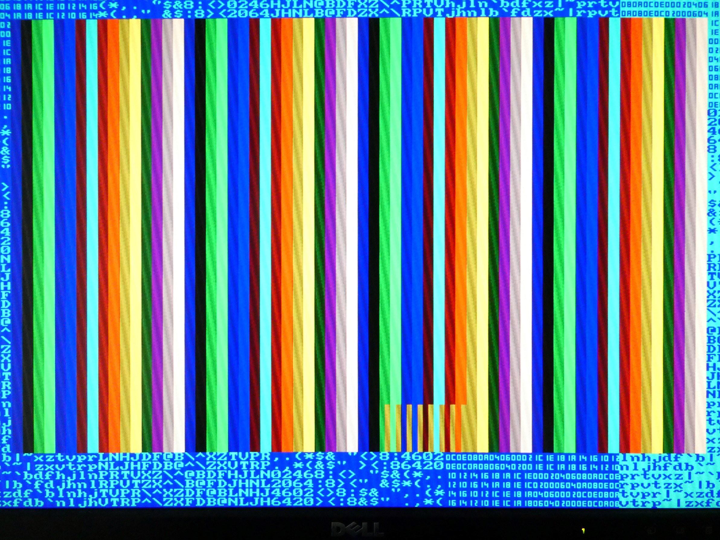
constant color_transparent:				std_logic_vector(7 downto 0):= "00000000";
constant color_medgreen: 					std_logic_vector(7 downto 0):= "00010000";
constant color_dkgreen:						std_logic_vector(7 downto 0):= "00001000";
constant color_dkblue:						std_logic_vector(7 downto 0):= "00000010";
constant color_medred:						std_logic_vector(7 downto 0):= "01100000";
constant color_dkred:						std_logic_vector(7 downto 0):= "01000000";
constant color_ltcyan:						std_logic_vector(7 downto 0):= "00001110";
constant color_dkyellow:					std_logic_vector(7 downto 0):= "10010000";
constant color_magenta:						std_logic_vector(7 downto 0):= "01100010";

constant color_black:			std_logic_vector(7 downto 0):= "00000000";
constant color_blue,	color_ltblue:	std_logic_vector(7 downto 0):= "00000011";
constant color_green,	color_ltgreen:	std_logic_vector(7 downto 0):= "00011100";
constant color_cyan:			std_logic_vector(7 downto 0):= "00011111";
constant color_red,	color_ltred:	std_logic_vector(7 downto 0):= "11100000";
constant color_purple:			std_logic_vector(7 downto 0):= "11100011";
constant color_yellow,	color_ltyellow: std_logic_vector(7 downto 0):= "11111100";
constant color_white:			std_logic_vector(7 downto 0):= "11111111";
constant color_ltgray:			std_logic_vector(7 downto 0):= "01101110";
constant color_dkgray,  color_gray:	std_logic_vector(7 downto 0):= "10010010";
With the modified Propeller test code (see below) this gives following colors (yellowish small bars on the bottom is my zombie sprite bug in Propeller code :-) ):
![]()
Note that "color 0" ("transparent") magically really works - the VDP simply decides to let the background color come through (first "dark blue") vertical bar in the VDP display window.
4. Test code update
Just a minimal change was needed, to see the 16 colors in action:
PRI _colorfulBlocks(color) |x, y, c
  c := 0
  repeat x from 0 to vdp.GraphicsHPixelCount - 1
    repeat y from 0 to vdp.GraphicsVPixelCount - 1
      if (color == vdp#TRANSPARENT)
        vdp.DrawPixel(x, y, x ^ y)
      else
        'vdp.DrawPixel(x, y, ColorPalette8[x & 7])
        vdp.DrawPixel(x, y, x & 15)
        c++
  vdp.WaitASecond
The x coordinate (which goes from 0 to 63) is used to set the color 0 ... 15.
No other code changes were done. But the results are much better than with the primitive 1-bit RGB A/D converter:
- 16 colors instead of 8
- no color bleeding or wrongly sampled pics
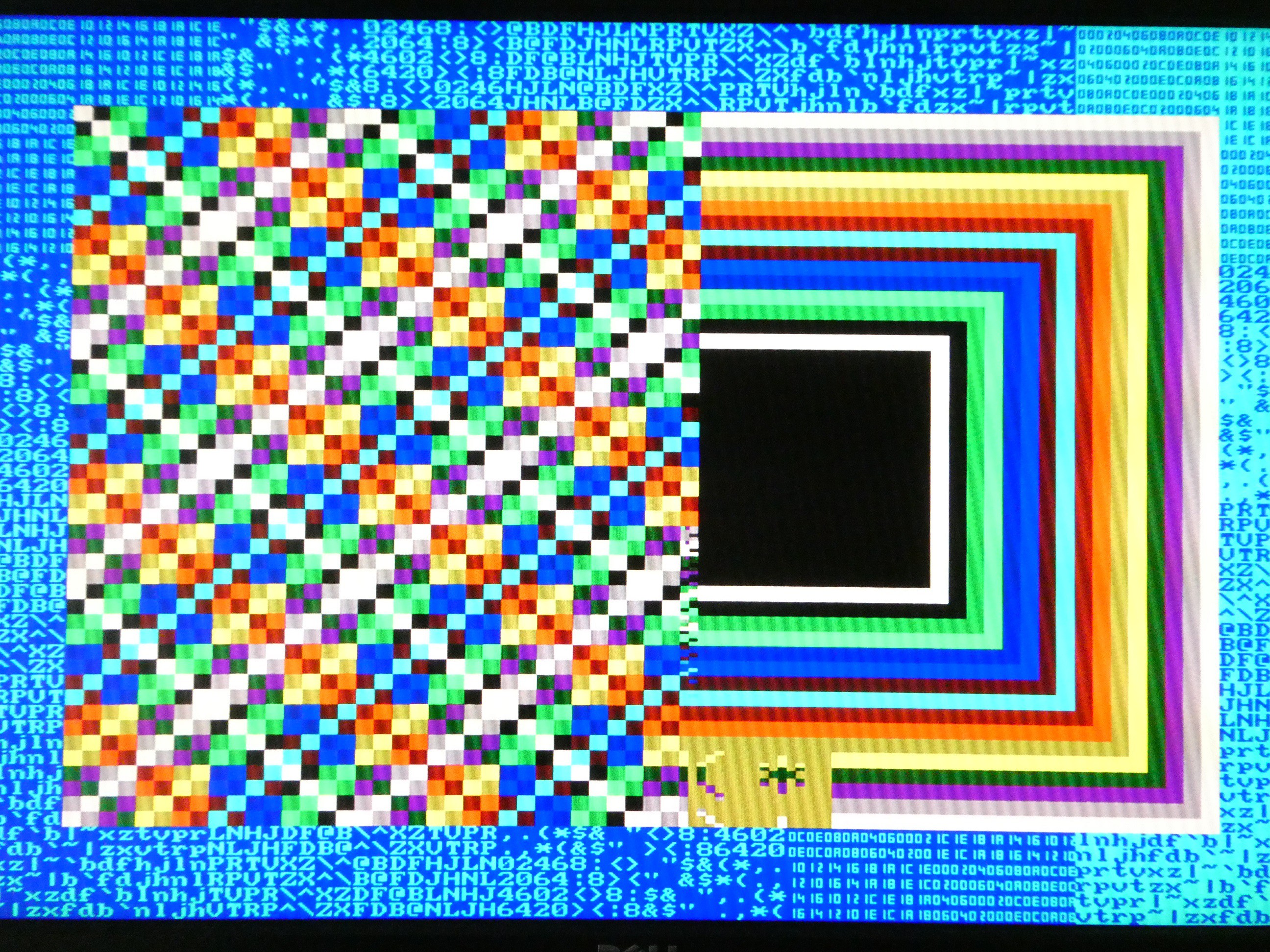
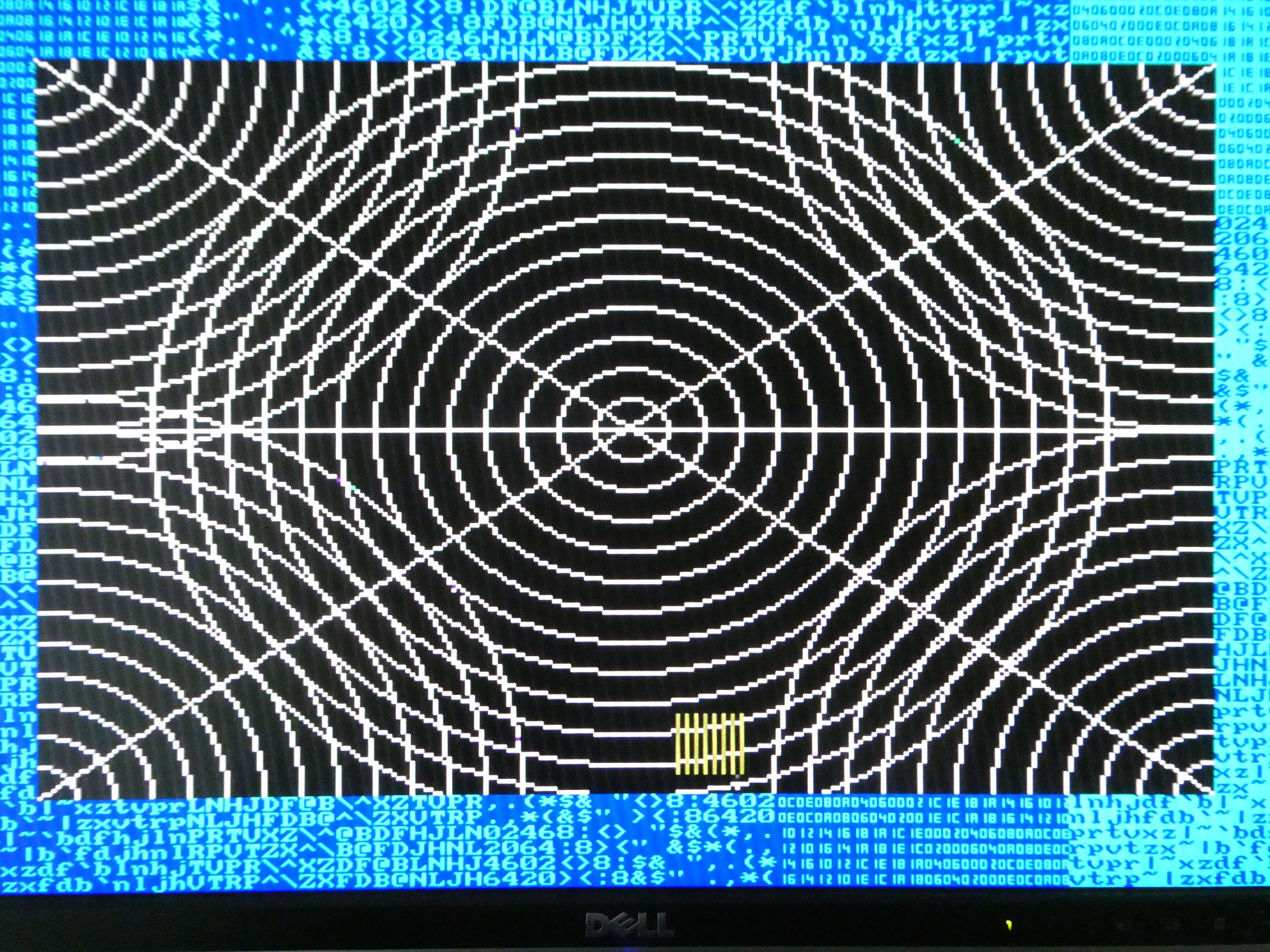
Here are some examples of demo screens using the color bus (lame pics of the screen, the actual quality is much better):
![]()
![]()
![]()
I have bugs with sprite patterns, but it can be observed that in case of scroll the VGA output can display the "picture in flux" - remember that sampler runs at VDP sync, and VGA at its own sync and they are completely async to each other.
![]()
5. Conclusion
Sampling the analog RBG outputs of V99X8 VDPs is possible and can lead to acceptable VGA picture, it requires higher quality A/D converters, PCBs and connections.
Sampling the color bus on the other hand leads to high-quality VGA sampling even with most basic hardware, essentially just direct wiring from VDP to FPGA.
I leave to some hardware wizard to create V99X8-based VGA board. In its simplest form, such board could contain only:
- V99X8
- FPGA (depending on the resources can contain VDP "dynamic" RAM, VGA "dual port" RAM, and the sampler / VGA controller described here)
- D/A VGA output circuit and connector
The board could be made to accept various "adapters" such as for RC2014, rosco_m68k, or even directly TMS9918 socket pinout (VGA for TI-99/4A!)
-
Future improvements
03/29/2021 at 04:41 • 0 commentsFrom the images and demo videos, it is obvious that the video quality is barely acceptable. There are two main problems:
- image sharpness - there is cross-bleeding of colors, noise artifacts etc.
- color resolution - only 8 basic colors are supported
Solutions for image sharpness
The flash A/D as I prototyped is very much a "chewing gum/duct-tape" solution, that can be improved in many ways:
- Put the circuit on a permanent solder board
- Keep wiring trimmed and matched
- Use higher quality potentiometers that allow finer and more stable regulation of threshold voltage
- Introduce external 21.47727MHz crystal to drive the sampler circuit instead of multiplying CPUCLK (which is XTAL/6) by 6 on FPGA
Solutions for color resolution
With 1-bit flash A/D per color channel only following colors can be supported:
RGB color 000 BLACK 001 DARK BLUE 010 DARK GREEN 011 CYAN 100 DARK RED 101 MAGENTA 110 DARK YELLOW 111 WHITE For a small improvement of resolution, for example from 1 to 2 bits, additional LM339 comparator per color channel could be used. However using 6 LM339s instead of 3 would not double the color resolution. Reason is that 2 LM339 set at 1/3 and 2/3 thresholds would produce 3 valid combinations:
00 no color 01 color intensity low 10 (ignore, as should not occur: if the higher LM339 is over the threshold, lower must be too) 11 color intensity high Still, 6-bit color digital vector obtained like this could be simply mapped at least to a valid 16-color table.
One additional interesting experiment would be to use the popular LM3914 dot-bar driver chip as a flash A/D. Theoretically, full 3-bit A/D conversion could be obtained from its 10 stage outputs.
-
Video conversion using dual port RAM in FPGA
03/29/2021 at 04:06 • 0 commentsThe basic approach is essentially the same as described here:
The key differences are:
TIM-011 V99X8 Resolution 512*256 256*192 (typically) Colors 4 (2 bit "intensity") 8 (1 bit per R, G, B) Pixels per byte 4
b7:b0 = VvVvVvVv2
b7:b0 = -RGB-RGBPixel clock 12MHz 5.3693175 Data sampler clock 48MHz 21.47727MHz Horizontal sync positive HSYNC, video signal has no porches positive HSYNC, video signal has front and back porch Vertical sync positive VSYNC, video signal has no porches regenerated from CSYNC, video signal has top and bottom porch Window on VGA 512*256 512*384 Memory used 32k 24k Refer to following files for key components:
This is the main top-level component. The video signals come in through 8-pin PMOD port:
alias VIDEO_HSYNC: std_logic is PMOD(7); -- BB6 on Anvyl (white)
alias VIDEO_CSYNC: std_logic is PMOD(6); -- BB5 on Anvyl (blue)
alias VDP_B_DIG: std_logic is PMOD(3);     -- "digitized" blue signal (using LM339 1-bit ADC)
alias VDP_G_DIG: std_logic is PMOD(2);     -- "digitized" green signal (using LM339 1-bit ADC)
alias VDP_R_DIG: std_logic is PMOD(1);     -- "digitized" red signal (using LM339 1-bit ADC)
alias VDP_CPUCLK: std_logic is PMOD(0);     -- v9958 pin 8 (XTAL/6 == 3.579545MHz)
(simplified here, the actual code contains overlapped signals for TIM-011 mode)
Out of these signals only VIDEO_HSYNC is directly used, as is a positive pulse that resets the horizontal scan counter and drives the vertical scan.
VIDEO_CSYNC:
Contains the VSYNC but also the HSYNC signals. To extract the VSNYC only a simple delay line is used that filters out a signal which is less than the length of HSYNC (24 pixels = 96 XTALs)
--generate VSYNC by filtering out HSYNC from CSYNC using a delay line
on_vdp_cpuclk: process(reset, VDP_CPUCLK, VIDEO_CSYNC, VIDEO_HSYNC)
begin
    if (rising_edge(VDP_CPUCLK)) then
        csync_line <= csync_line(30 downto 0) & VIDEO_CSYNC;
    end if;
end process;

vdp_vsync <= not (VIDEO_CSYNC or csync_line(17)); -- 24 pixels long ~ 17 CPUCLK
VDP_CPUCLK:
This the master used for sync of pixel clock. The frequency is XTAL/6. So to get XTAL, we multiply by 12 (using a built-in DCM "digital clock manager" circuit baked into the Xilinx FPGA. Almost all FPGAs support similar (or PLL) circuits to generate clocks of almost any frequency). However multiplying with 12 is not perfect, it is noticeable in vertical bars that appear when digitizing the R, G, B signals.
The clock produced (42.95454 MHz) is then divided by 2 but also used to drive delay lines for digitized R, G, B:
on_vdp_xtal_int2: process(VIDEO_HSYNC, vdp_xtal_int2, VDP_R_DIG, VDP_G_DIG, VDP_B_DIG, r_line, g_line, b_line)
begin
--	if (VIDEO_HSYNC = '1') then
--		vdp_xtal_int <= '0';
--	else
		if (rising_edge(vdp_xtal_int2)) then
			vdp_xtal_int <= not vdp_xtal_int;
			r_line <= r_line(6 downto 0) & VDP_R_DIG;
			g_line <= g_line(6 downto 0) & VDP_G_DIG;
			b_line <= b_line(6 downto 0) & VDP_B_DIG;
		end if;
--	end if;
end process;
VDP_R_DIG, VDP_G_DIG, VDP_B_DIG:
These are the "raw" 1-bit color signals from LM339. But they are not directly fed to the sampler, a bit of timing tweak is possible by tapping into the delay line. This allows removing some noise to sample the video signals at a precise moment.
r_delayed <= r_line(to_integer(unsigned(switch(7 downto 6) & '1')));
g_delayed <= g_line(to_integer(unsigned(switch(5 downto 4) & '1')));
b_delayed <= b_line(to_integer(unsigned(switch(3 downto 2) & '1')));
Six switches on the Mercury baseboard select the moment to sample the color signal.
With these signals ready, they are fed into the "sampler" component:
offset_vdp <= button(3 downto 0) when (switch_tms = '1') else "0000";
vdp: vdp_sampler2 port map (
		reset => RESET,
		clk => vdp_xtal_int, --
		hsync => VIDEO_HSYNC,
		vsync => vdp_vsync,
		pixclk => vdp_pixclk,
		offsetclk => freq4,
		offsetcmd => offset_vdp, -- in TMS mode move the 0, 0 dot within the window
		r => r_delayed, --VDP_R_DIG,
		g => g_delayed, --VDP_G_DIG,
		b => b_delayed, --VDP_B_DIG,
		a => vdp_sampler_a,
		d => vdp_vram_dina,
		limit => "001110", --switch_limit,
		we_in => we_in,
		we_out => vdp_sampler_wr_nrd
	);
The sampler takes following inputs:
- video signals from V9958 conditioned as described above
- "offset" which is a command to increment / decrement internal register that determines when the pixel signals start
- "limit" is a constant that determines the timing when to take sample of pixel and write to dual-RAM
Outputs:
- a - address to dual-RAM
- d - data to be written to dual-RAM
- we_out - write enable to dual-RAM
The "sampler" circuit is relatively simple. The key to remember is:
4 XTAL = 1 pixel ("sample_pulse")
2 pixel = 1 byte ("write_pulse")
8 XTAL = 1 byte
So in 8 input clock cycles, the R, G, B signals have to be sampled twice and byte containing the xRGBxRGB written once:
-- 8 xtal cycles == 2 pixel clock == 1 byte
on_clk: process(clk, hsync, cnt, r, g, b)
begin
	if (hsync = '1') then
		cnt <= "000";
	else
		if (falling_edge(clk)) then
			cnt <= std_logic_vector(unsigned(cnt) + 1);
		end if;
	end if;
end process;

pixclk <= cnt(1);
write_pulse <= (limit(5) xor clk) when (cnt = limit(2 downto 0)) else '0';
sample_pulse <= (limit(5) xor clk) when (cnt(1 downto 0) = limit(4 downto 3)) else '0';
The exact timing when this happens in 8 cycle sequence is determined by parameter "limit" set as constant from outside (it is somewhat tweakable).
The "sample" pulse drives a shift register that moves by 4 bits (note that MSB is set as '0'), and lower 3 bits capture the RGB color:
on_sample_pulse: process(sample_pulse, r, g, b, sample)
begin
	if (rising_edge(sample_pulse)) then
		sample <= sample(3 downto 0) & '0' & r & g & b;
	end if;
end process;
How is the sampled color byte (containing 2 pixels) stored in the memory?
The scan line is typically 256 pixels, which means 128 bytes, 7 bits. And then there are 192 rows which fits in 8 bits. So the 14-bit address is:
VVVVVVVVHHHHHHH
-- output signals
d <= sample;

a <= v_off(7 downto 0) & h_off(7 downto 1);
we_out <= write_pulse and (not h_off(8)) and (not v_off(8));

-- offset to ignore "left" before real pixel data comes in
h_off <= std_logic_vector(unsigned(h) + unsigned(h_offset(8 downto 0)));--unsigned(limit(2 downto 0) & "00"));
-- offset to ignore "top" before real pixel data comes in
v_off <= std_logic_vector(unsigned(v) + unsigned(v_offset(8 downto 0)));--unsigned(limit(5 downto 3) & "00"));
v_ok <= '0' when (unsigned(v_off) > 191) else '1';
However, the V and H are not direct horizonatal or vertical counters. The pixels do not start right after VSYNC and HSYNC signals, there are "porches" that delay the start. So both directions have offsets that can be tweaked using 2 up/down counter registers:
h_reg: offsetreg Port map ( reset => reset, initval => "1111100110", -- -26 (0x3E6) mode => offsetcmd(1 downto 0), clk => offsetclk, sel => '0', outval => h_offset ); v_reg: offsetreg Port map ( reset => reset, initval => "1111100101", -- -27 (0x3E5) mode => offsetcmd(3 downto 2), clk => offsetclk, sel => '0', outval => v_offset ); -
Driving V9958 using Propeller
03/29/2021 at 04:05 • 0 commentsThe Propeller spin code used to drive the design for test purposes has been written years ago, for a different project:
However, it could be repurposed here with only minimal changes. That was possible because:
- V99X8 VDPs are truly backward compatible with TMS9918
- No special 99X8 modes are being used
- No extended registers are being used (only single address line is used)
Parallax Propeller is a very powerful chip - it contains 8 32-bit CPUs that can control 32-bit I/O pins. This allows direct interfacing with legacy chips in speed ranges below 10MHz or so. Beside VDPs, for example I was able to drive a Am9511 FPU too.
This project has only 2 files:
This is the VDP driver. It is interfacing the physical pins and drives them as if the VDP is on a bus of a microcomputer.
CON
'Signal     Propeller pin   VDP pin ( == F18A pins)
nRESET =    27'12'             34 == pull low for reset
MODE =      26'11'             13 == memory/register mode
nCSW =      25'10'             14 == write to register or VDP memory
nCSR =      24'9'      '       15 == read from register or VDP memory
nINT =      23'8'              16 == input always, activated after each scan line if enabled
CD0 =       7'              24 == MSB (to keep with "reverse" TMS99XX family documentation)
CD1 =       6'              23
CD2 =       5'              22
CD3 =       4'              21
CD4 =       3'              20
CD5 =       2'              19
CD6 =       1'              18
CD7 =       0'              17 == LSB
'VSS                        12 == GND
'VCC                        33 == +5V
Programming the Propeller has many interesting aspects, one of the most important ones is how to make multiple CPUs ("cogs") work in parallel. Each cog can drive own pins, but when the cog is stopped, those pins are "released". To ensure the pins toward VDP are constantly driven, a cog is initialized and then kept in a "dead loop".
The public "Start" method communicates the shared memory (described later) and after some housekeeping kicks off the _vdpProcess() routine in a new cog.
PUB Start(plCommandBuffer, initialMode, useInterrupt, enableTracing) : success

  longfill(@stack, 0, STACK_LEN)
  skipTrace := true
  if (enableTracing)
    pst.Start(115_200)
    pst.Clear
    skipTrace := false

  Stop

  plCommand := plCommandBuffer
  longfill(@spriteSpeed, 0, 32)
  colorGraphicsForeAndBack := byte[@GoodContrastColorsTable]

  _prompt(String("Press any key to continue with TMS9918 object start using command buffer at "), plCommand)

  lockCommandBuffer := locknew
  if (lockCommandBuffer == -1)
    _logError(String("No locks available to start object!"))
    return false
  else
    cogCurrent := cognew(_vdpProcess(initialMode, useInterrupt), @stack)
    if (cogCurrent == -1)
      _logError(String("No cogs available to start object!"))
      lockret(lockCommandBuffer~)
      return false
  waitcnt((clkfreq * 1) + cnt)
  _logTrace(String("TMS9918 object launched into cog "), cogCurrent, String(" using lock "), lockCommandBuffer, String(" at clkfreq "), clkfreq, 0)
  return true
The cog now runs the routine until it exists or other cog kills it from outside. The _vdpProcess() does the following:
- initialized the pins (input / output)
- fills the video memory (clears 16k)
- sets initial video mode
After that, it goes into an infinite loop of watching for a command and its parameters, and if received executes them. This is very similar to Window message processing paradigm: as long as the window exists, it has a "message pump" that accepts commands sent to it and execute them (one can even say that cog is the "hWnd").
The commands are "longs" (32-bit) values written to common RAM memory area. This is again similar to Windows CMD, lParam and wParam mechanism, but to simplify, the number of parameters here are flexible based on the command:
PRI _vdpProcess(initialMode, useInterrupt) |i, y, timer
  _logTrace(String("TMS9918 object starting in cog "), cogId, String(" using lock "), lockCommandBuffer, String(" at clkfreq "), clkfreq, 0)

  nextCharRow := 0
  nextCharCol := 0
  if (useInterrupt)
    vdpAccessWindow := ((((clkfreq / 60) * (262 - 192)) / 262) * 95) / 100 'see table 3.3 in TMS9918 documentation (we have 70 scan lines every 1/60s)
  else
    vdpAccessWindow := clkfreq / 60
  _logTrace(String("Initial mode is "), initialMode, String(" use interrupt is "), useInterrupt, String(" vdp access clock cycles is "), vdpAccessWindow, 0)

  outa[nReset .. CD7]~~         'set all to 1 (inactive)
  dira[nReset .. CD7]~          'set all to input first
  dira[nReset .. nCSR]~~        'these are always outputs
  _vdpReset
  _setReg(1, reg[1] & %1011_1111) 'blank screen
  lastStatus := _readStatus
  _fillVdpMem(0, 16 * 1024, 170, 0) '10101010 pattern
  'this is the first command that will be executed
  long[plCommand][0] := CMD_SETMODE
  long[plCommand][1] := initialMode
  displayMode := initialMode
  longfill(@lastSpritePositionUpdateCnt, cnt, 32)
  repeat  'keep executing commands until cog is stopped
    repeat until not lockset(lockCommandBuffer) 'wait for the free lock (don't execute while command buffer is updated)

    'update position of even numbered sprites according to their speed, if set
    _updateSpritePositions(0)

    timer := cnt
    case LONG[plCommand]
      CMD_SETSPRITEMODE:
        _setSpriteMode(long[plCommand][1] & %0000_0011)
        '_logCommand(String("CMD_SETSPRITEMODE in mode "), _interval(cnt, timer))

... (OTHER COMMANDS)
This mechanism could allow:
- FIFO buffering of commands (the driver component can work async and "stuff" commands to some preset depth and continue processing while the VDP cog executes)
- Multiple cogs can interface independently with various chips - with enough pins, 2 VDPs can be driven independently etc.
Let's see how a sample command is executed, for example drawing a circle:
      CMD_DRAWCIRCLE:
        _drawCircle(long[plCommand][1], long[plCommand][2], long[plCommand][3], long[plCommand][4])
        '_logCommand(String("CMD_DRAWCIRCLE in mode "), _interval(cnt, timer))
Circle takes 4 parameters which are the coordinates of the center, radius, and color (which can be 0 or 1 in hi-res, or 0-3 in multicolor modes)
PRI _drawCircle(xc, yc, radius, color) |x, y, x2, y2, r2, x2m, pixCount
  '_logTrace(String("Drawing circle in color "), color, String(" at "), xc << 16 | yc , String(" with radius "), radius, 8)
  if (radius < 1)
    return 0
  pixCount := 0
  x := radius
  y := 0
  r2 := radius * radius
  x2 := r2
  y2 := 0
  repeat while (y =< x)
    pixCount += _drawPixel(xc + x, yc + y, color)
    pixCount += _drawPixel(xc + x, yc - y, color)
    pixCount += _drawPixel(xc - x, yc + y, color)
    pixCount += _drawPixel(xc - x, yc - y, color)
    pixCount += _drawPixel(xc + y, yc + x, color)
    pixCount += _drawPixel(xc + y, yc - x, color)
    pixCount += _drawPixel(xc - y, yc + x, color)
    pixCount += _drawPixel(xc - y, yc - x, color)
    y2 := y2 + y + y + 1
    y++
    x2m := x2 - x - x + 1
    if (_circleError(x2m, y2, r2) < _circleError(x2, y2, r2))
      x--
      x2 := x2m
On the bottom of the execution stack are the routines that drive the VDP signals in order to write command or data, or read status or data, including generating a reset:
{{ interfacing with VDP chip }} PRI _readStatus return _vdpRead(1) PRI _vdpRead(modeVal) if (modeVal == 0) 'only wait if reading from vdp memory, not status reg _waitForScan outa[MODE] := modeVal 'set mode outa[nCSW]~~ 'write inactive outa[nCSR]~~ 'read inactive dira[CD0 .. CD7]~ 'data bus is input outa[nCSR]~ 'pulse nCSR result := ina[CD0 .. CD7] outa[nCSR]~~ PRI _vdpWrite(byteVal, modeVal) if (modeVal == 0) 'only wait if writing to vdp memory, not register _waitForScan outa[MODE] := modeVal 'set mode outa[nCSW]~~ 'write inactive outa[nCSR]~~ 'read inactive dira[CD0 .. CD7]~~ 'data bus is output outa[CD0 .. CD7] := byteVal outa[nCSW]~ 'delay outa[nCSW]~~ PRI _vdpReset outa[nReset]~ waitcnt((clkfreq / 2) + cnt) '500ms outa[nReset]~~In Propeller parlance, this is the "top level" object code, that is started up at boot time. Its purpose is to exercise various modes and options of the VDP to show its working on the screen. As a parameter, it takes the state of 4 switches on the Propeller demo board to either run all the demos or generate test picture to adjust the colors (== screwdriver and potentiometers!) or timings (== switches on FPGA board):
PUB Main | mode, rnd, switches
  waitcnt((clkfreq * 4) + cnt) 'wait 4s before start

  if vdp.Start(@CommandBuffer, vdp#GRAPHICS1, false, true)

    repeat true
      'read switches and if color is TRANSPARENT (== 0) continue with demo, otherwise show solid color screen
      dira[13..10]~ 'set as input
      switches := ina[13..10]
      if (switches < 8)
        vdp.Trace(String("Switches are in COLOR (< 8) mode, displaying 8 vertical color bars for calibration "), switches)
        vdp.SetMode(vdp#MULTICOLOR)
        _colorfulBlocks(byte[@ColorPalette8][switches])
      else
        if (switches > 8)
          vdp.Trace(String("Switches are in TICK (> 8) mode, tick lines (every 8 pixels) "), switches)
          vdp.SetMode(vdp#GRAPHICS2)
          _tickLines(byte[@ColorPalette8][switches - 8])
        else
          vdp.Trace(String("Switches are in DEMO (== 8) mode, all running demos "), switches)
          repeat mode from vdp#TEXT to vdp#GRAPHICS1

(demo cases)
Here is for example a demo that generated 8 sprites and sets them wandering across the screen in various directions:
PRI _spriteDemo(char, waitSecs) |dx, dy, i, rnd
  vdp.SetSpriteMode(vdp#SPRITESIZE_16X16 | vdp#SPRITEMAGNIFICATION_2X)
  repeat i from 0 to 7
    vdp.GenerateSpritePatternFromChar(@SpriteTestPattern16, char + i, 32)
    vdp.SetSpritePattern(i * 4, @SpriteTestPattern16, 32)
    vdp.SetSprite(i, vdp#SPRITEMASK_SETPATTERN | vdp#SPRITEMASK_SETCOLOR | vdp#SPRITEMASK_SETX | vdp#SPRITEMASK_SETY, i * 4, vdp.SpriteHPixelCount / 2 - 16, vdp.SpriteVPixelCount / 2 - 16, 15 - i)
  'give speed vectors to sprites and let send them off autonomously
  vdp.SetSprite(0, vdp#SPRITEMASK_VX | vdp#SPRITEMASK_VY, 0,  1,  0, 0)
  vdp.SetSprite(1, vdp#SPRITEMASK_VX | vdp#SPRITEMASK_VY, 0,  1, -1, 0)
  vdp.SetSprite(2, vdp#SPRITEMASK_VX | vdp#SPRITEMASK_VY, 0,  0, -1, 0)
  vdp.SetSprite(3, vdp#SPRITEMASK_VX | vdp#SPRITEMASK_VY, 0, -1, -1, 0)
  vdp.SetSprite(4, vdp#SPRITEMASK_VX | vdp#SPRITEMASK_VY, 0, -1,  0, 0)
  vdp.SetSprite(5, vdp#SPRITEMASK_VX | vdp#SPRITEMASK_VY, 0, -1,  1, 0)
  vdp.SetSprite(6, vdp#SPRITEMASK_VX | vdp#SPRITEMASK_VY, 0,  0,  1, 0)
  vdp.SetSprite(7, vdp#SPRITEMASK_VX | vdp#SPRITEMASK_VY, 0,  1,  1, 0)
  repeat waitSecs
    vdp.WaitASecond
It is interesting to note that vdp.SetSprite() function is executed by the "current cog", not the one driving the VDP. But the execution is really just preparing the command and parameters to be written to common RAM (all cogs share common RAM, accessed on round-robin basis), after which the SetSprite() function exists. The VDP cog then reads the command from common RAM and drives the sprite across the screen:
PRI _setSprite(spriteId, mask, patternId, x, y, color) |spriteAttributeAddress spriteAttributeAddress := SpriteAttributeTable + (spriteId << 2) _copyFromVdpMem(spriteAttributeAddress, @SpriteBuff, 4) '_logSprite(String("Sprite before "), spriteAttributeAddress, @SpriteBuff) if (mask & SPRITEMASK_SETY) byte[@SpriteBuff][0] := y else if (mask & SPRITEMASK_DY) byte[@SpriteBuff][0] += y else if (mask & SPRITEMASK_VY) byte[@spriteSpeed + (spriteId << 1)][1] := y if (mask & SPRITEMASK_SETX) byte[@SpriteBuff][1] := x else if (mask & SPRITEMASK_DX) byte[@SpriteBuff][1] += x else if (mask & SPRITEMASK_VX) byte[@spriteSpeed + (spriteId << 1)][0] := x if (mask & SPRITEMASK_SETPATTERN) byte[@SpriteBuff][2] := patternId if (mask & SPRITEMASK_SETCOLOR) byte[@SpriteBuff][3] := (byte[@SpriteBuff][3] & $F0) | (color & $0F) '_logSprite(String("Sprite after "), spriteAttributeAddress, @SpriteBuff) _copyToVdpMem(spriteAttributeAddress, @SpriteBuff, 4) -
Flash A/D converter for analog R, G, B
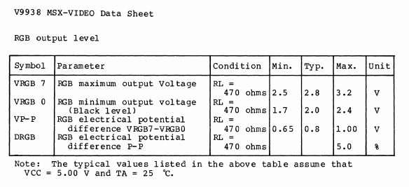
03/29/2021 at 04:04 • 0 commentsUnlike their TMS99X8 video display ancestors used in MSX (and many other home computers and game consoles), the Yamaha V9938 / V9958 VDPs generate analog R, G, B along with sync signals:
Variation Output Input DRAM TMS9918A 60Hz NTSC composite 60Hz NTSC composite 16k x 1bit TMS9928A 60Hz YPbPr 16k x 1bit TMS9929A 50Hz YPbPr 16k x 1bit TMS9118 60Hz NTSC composite 60Hz NTSC composite 16k x 4bit TMS9128 60Hz YPbPr 16k x 4bit TMS9129 50Hz YPbPr 16k x 4bit The voltage level on RGB outputs is in the following range:
![]()
The threshold voltage level must be set somewhere above VRGB0 and below VRGB7 - matched to the specific VDP driving the circuit.
To feed the FPGA with digital R, G, B, an A/D converter is needed. There are two main concerns here:
- speed: the pixel clock is XTAL/4 = 21.47727/4 = 5.3693175MHz. This means the A/D conversion must complete in time much less than 185ns
- resolution: the absolute minimum needed is 1 bit - color is present or not
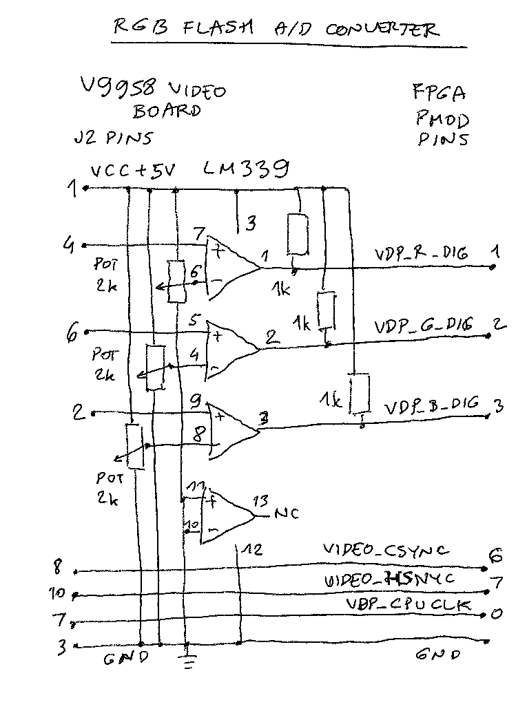
One could of course use fast, high-precision, and expensive A/D converters. But for the proof of concept purposes, a super cheap voltage comparator circuit is sufficient:
![]()
When the voltage LM339 on + input is greater than - input, the output is "high" - meaning color is detected.
The voltage cutoff point is determined by running the demo code and and tweaking the potentiometer positions with a screwdriver until the colors looks acceptable:
The 1k pull-up resistors are pure ad-hoc improvisations too, prototyping the circuit on the breadboard I found that having them increases the picture quality, probably by generating faster output rise times.
Other signals are directly led from VDP to FPGA:
- VIDEO_CSYNC - this signal contains both VSYNC and HSYNC components. The VSYNC is extracted in the FPGA from it. VSYNC frequency is 15.7kHz/262 = 60Hz.
- VIDEO_HSYNC - positive pulse denotes start of new scan line. The frequency is XTAL/ 1368 = 15.7kHz
- VDP_CPUCLK - this is XTAL/6 = 3.579545MHz signal. It is used to multiply with 12/2 in order to regenerate XTAL frequency inside the FPGA
![]()
-
Test rig
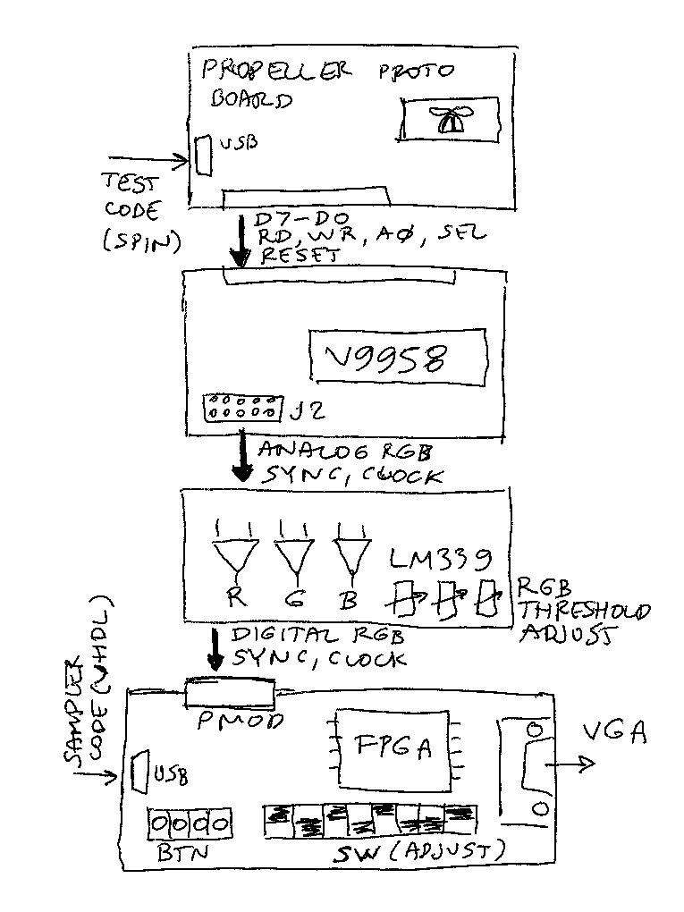
03/29/2021 at 04:02 • 0 commentsThe sketch below describes key hardware components of this proof of concept:
Propeller proto-board
This board is out of production, but any proto-board with Propeller can be used. It is convenient that the number of signals that need to be driven is small: 8 data + 4 control lines only. So smaller boards with 16 connections to the breadboard are sufficient.
V9958 board
I used the high-quality kit board originally meant for rosco-m68k MC68000 computer. Few small hardware hacks were needed because the board adapter is set for MC68000 bus (J1), and Propeller allow direct interfacing with VDP, without glue logic. So I removed one GAL from the board, and connected the /RD and /WR signals directly, bypassing the Motorola bus R/nW logic.
I use the J2 output pins to tap into the VDP signals (not the DIN output)
Flash A/D board
This one is described separately, but is nothing more than 3 voltage comparators with potentiometers to tweak voltage cutoff separately for R, G, B and some pull up resistors on outputs. The result is RBG 3-bit digital color signal.
FPGA board
I used Mercury FPGA, a very convenient, economical and high quality board from MicroNova. Older Xilinx FPGA chip can be programmed using old but free ISE14.7 IDE, and the baseboard has VGA output. The signals are coming through PMOD. PMOD has 8 I/O pins, in this case 6 are used, 3 for RGB and 3 for control signals (HSYNC, CSYNC, CPU_CLOCK = XTAL/6)
![]()
MSX2(+) video to VGA conversion (proof of concept)
V9938 and V9958 Video display processors were successors to TMS99X8 - this is an attempt to convert their video signal to VGA using FPGA