 David H Haffner Sr
-
Assembling The ATmega1284/MCU CHASSIS CASE / SEC I
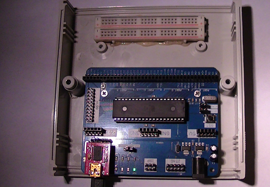
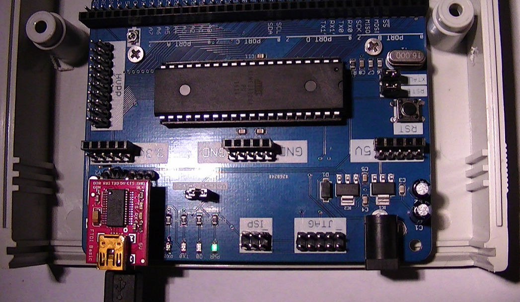
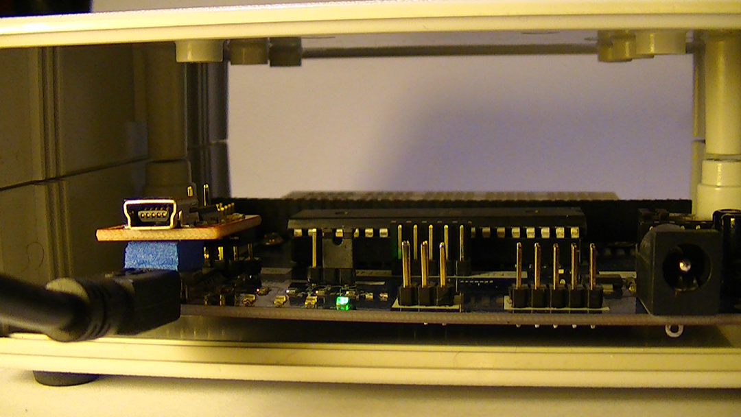
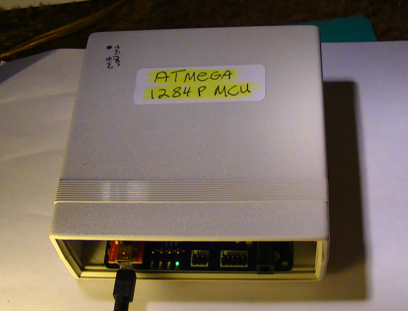
03/08/2017 at 17:15 • 0 commentsThese are the first assembly pics for the ATmega1284P/MCU (development board courtesy of MCUdude @Tindie ) http://www.tindie.com/products/MCUdude/dip-40-arduino-compatible-development-board/
The main controller hardware will be housed in a
1598-BSGY
GREY CHASSIS CASE 5.26" X 5.3" X 2"
![]()
The board when shipped, comes with an ATmega32 already to go, so I just removed that and replaced it with the ATmega1284 and burned the bootloader, everything so far, seems ok with the new chip.
![]()
![]()
![]()
-
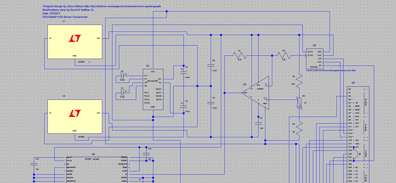
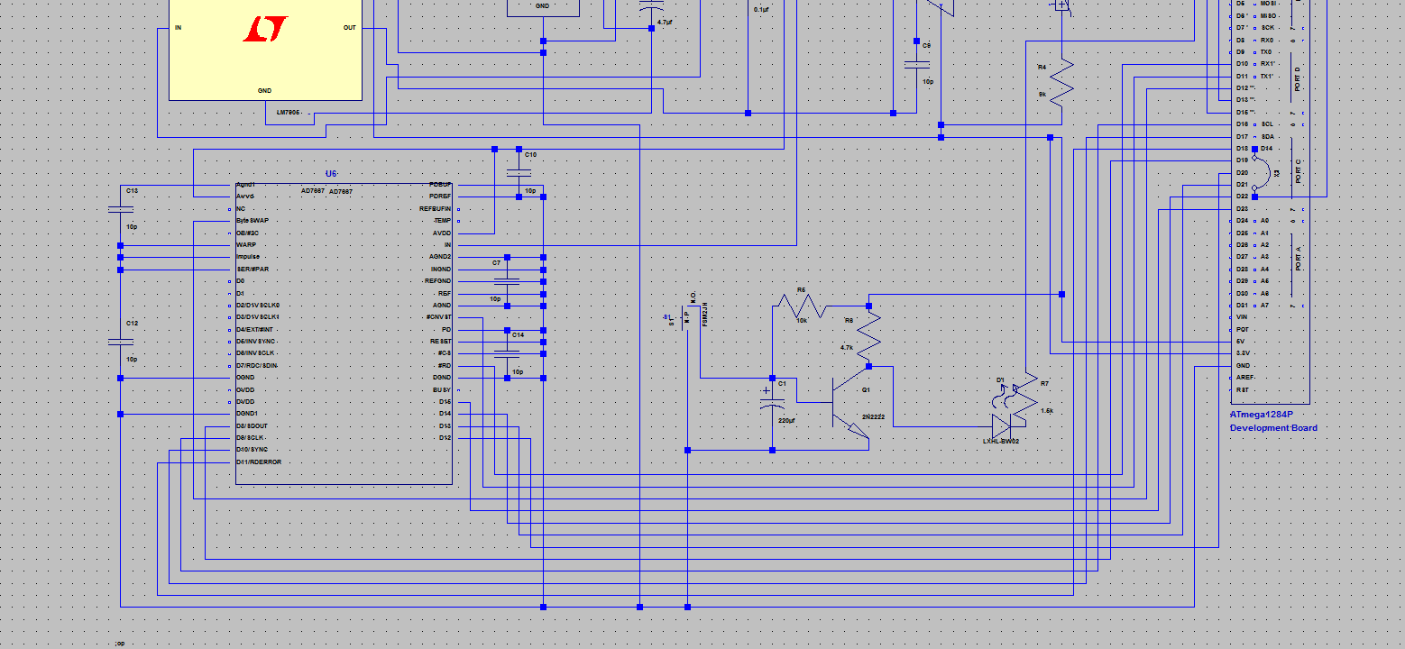
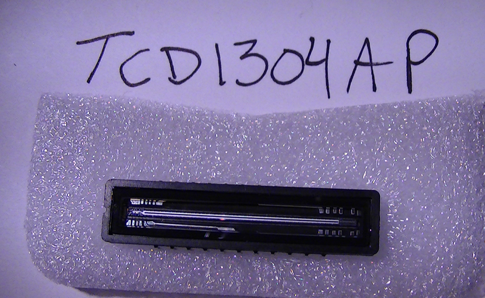
Final Schematic/CCD Driver Circuit/TCD1304AP REV C
03/05/2017 at 16:33 • 0 commentsThis is the final schematic design for the CCD driver circuit, this design was originally made by David Allmon at http://davidallmon.com/pages/ad7667-spectrograph , I have made my own mods because it has to work with my spectrometer, but the circuit works fine. David has emailed me and verified that it works, and that my modifications are fine also, so a big green light!
When I get the rest of my parts in, I will be documenting the build, because there are a few more mods to make so both the TCD1304 circuit and MCU can interface together.
![]()
![]()
![]()
The .asc files will be available on my files page for all schematics for download (LTspice.)
-
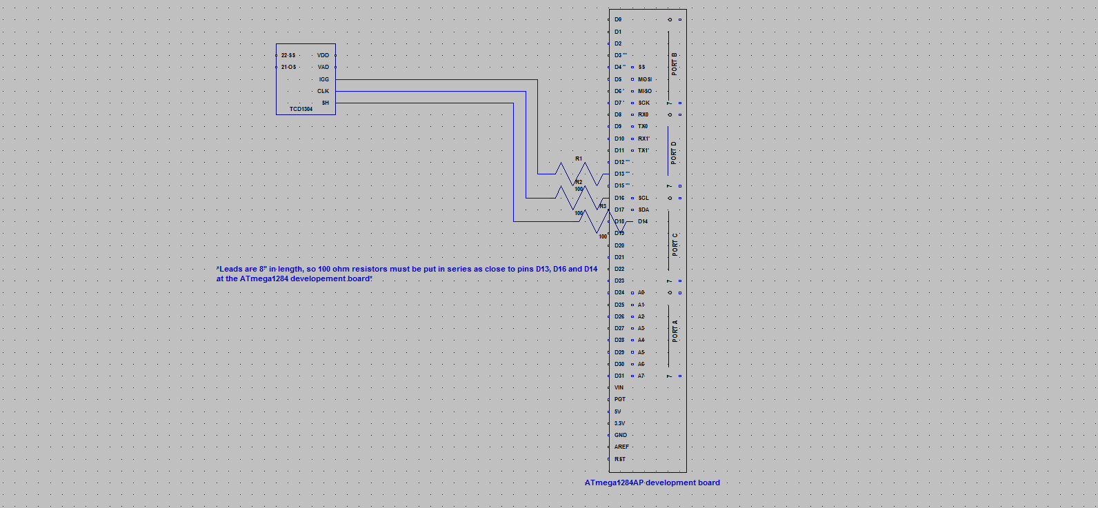
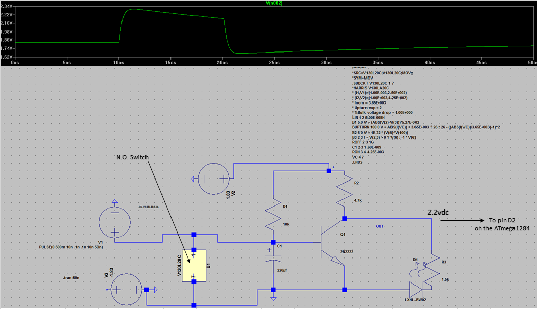
Added Switch Debouncer @ S1 on Schematic/CCD Driver Circuit
03/04/2017 at 13:25 • 0 comments*UPDATE* 3/4/2017 3:16:PM
I redid the SIM for the switch debouncer for S1, I included the LED indicator with its resistor to make sure the values stayed the same, do not mind the component at U1, I included it there because I needed a component to complete the circuit when it is closed and the components in the .LIB files are not cuttin' it. So it's just there to complete the circuit.
![]()
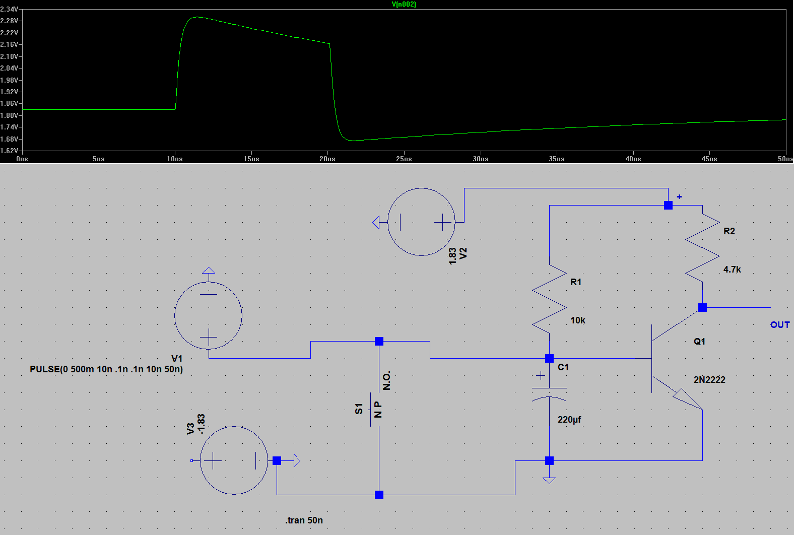
I added a simple single trigger switch debouncer at S1 on the main schematic for the CCD driver circuit, because this is the last stop where the frame data is waiting for upload.
![]()
The 220uf cap is to lock out S1 for 1 second after the pulse, since there will be another frame waiting in the wings.
-
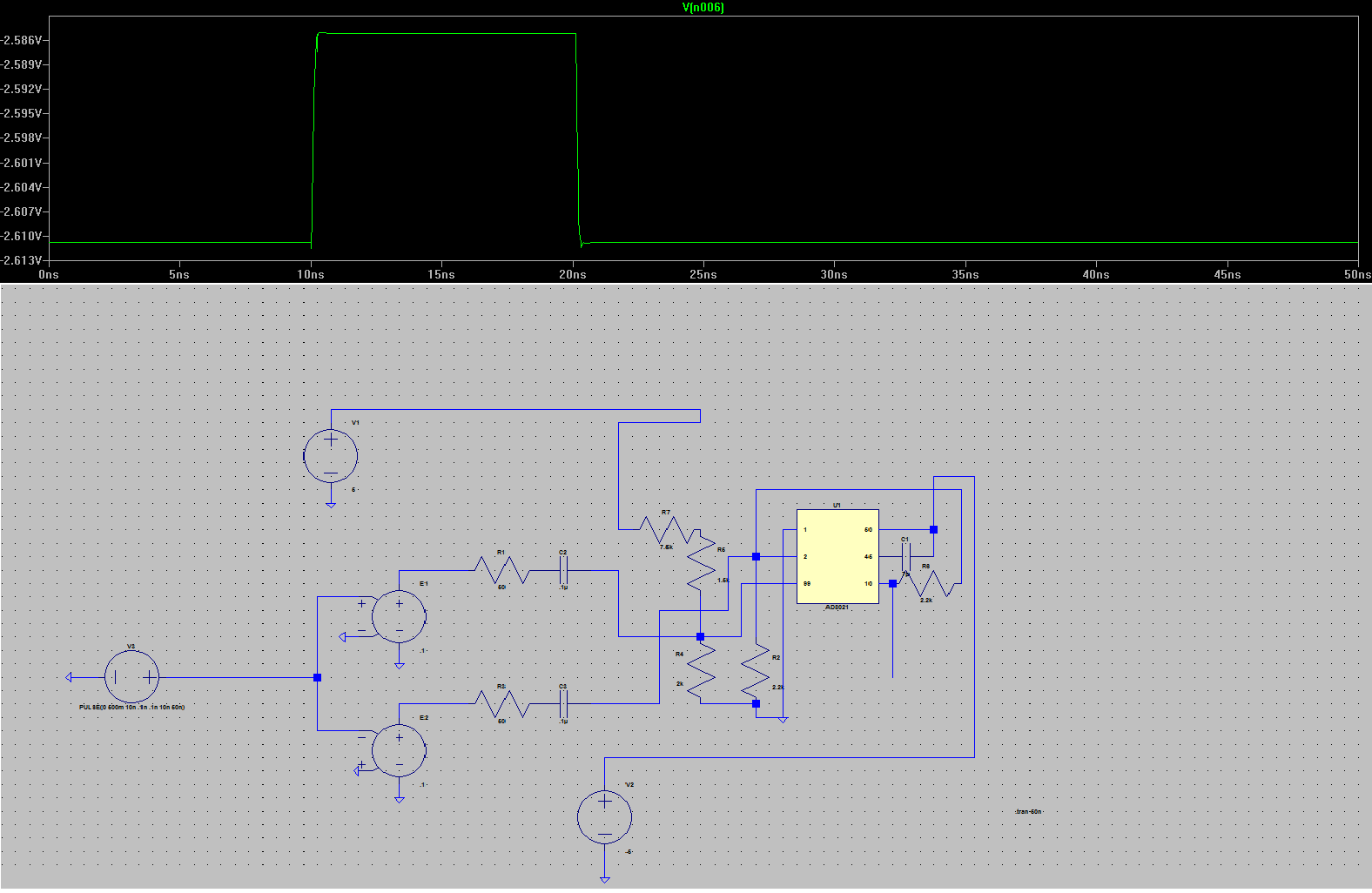
*UPDATED SIM* LTspicemodel/ AD8021 re-configured...
03/02/2017 at 23:52 • 0 commentsHere is the new spicemodel sim, I experimented with several resistor schemes to get the 9.09k value at R5 on the schematic and settled on 2 resistors; 1.5k and a 7.5k in series at R5. This takes care of that ringing spot on the rise time in the SIM. (the .ASC file will be updated on my page.)
![]()
![]()
-
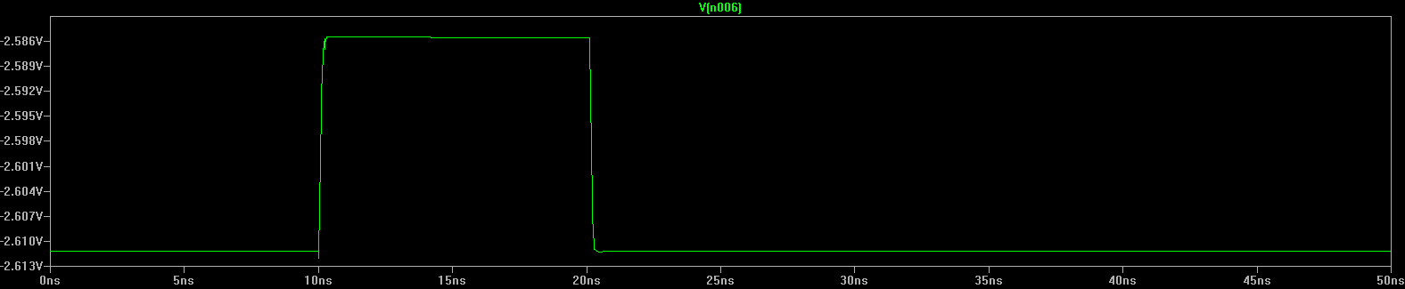
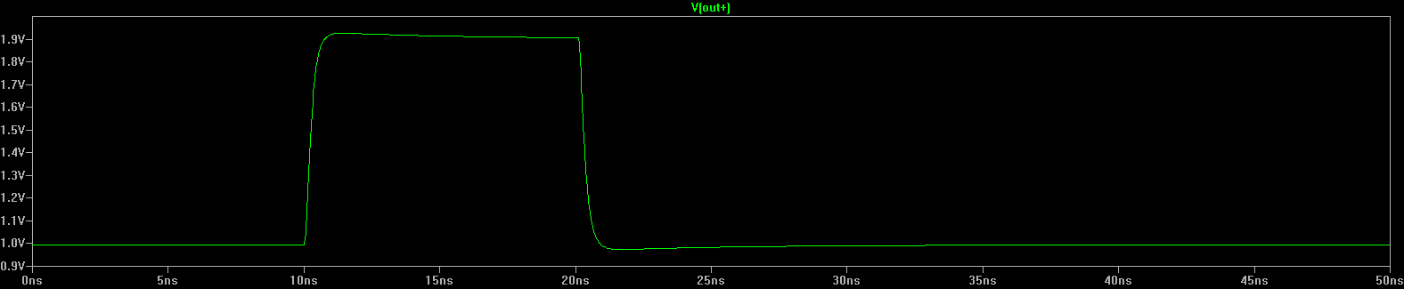
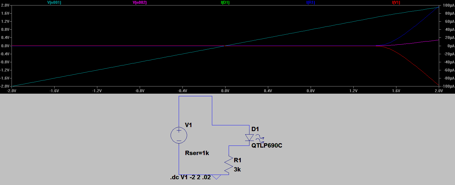
Need Some Help...Simulating the AD8021 op-amp/W/LTspice
03/01/2017 at 14:03 • 7 comments*UPDATED* well I just found out why there is a 9.09k resistor @ R5 on the schematic, it gets rid of that "ringing" at the peak at rise time @ 10ns pulse.
![]()
Thanks to @Ted Yapo for helping me fix this simulation on LTspice. The "real" op amp is in place -AD8021,
the true parameters are inputted at the pulse generator (pins 7 and 8, are not present, for some reason spicemodel file omitted them for error?) so I'm not worrying about it for now, I just needed to know that the output at pin 6 is -2.5v when R4 (which is a trimmer pot 2k,) is adjusted to 1.83v.
![]()
The .ASC file will be available for this sim on my files page.
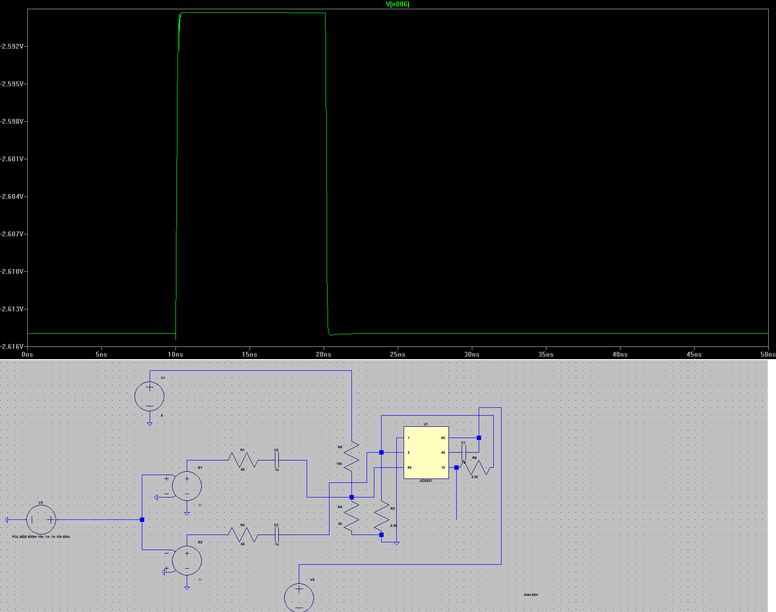
I corrected some of the pulse generator values to what they are exactly on the data sheet and schematic, 10um and 20um. Something still doesn't look right, from rise time to fall time. Also I just wanted to add that, I may be spending a lot of extra time on this aspect of my build, but I have learned through experience that, it is better to build it right the first time, so I don't have to de-solder everything and do it over again!
![]()
![]()
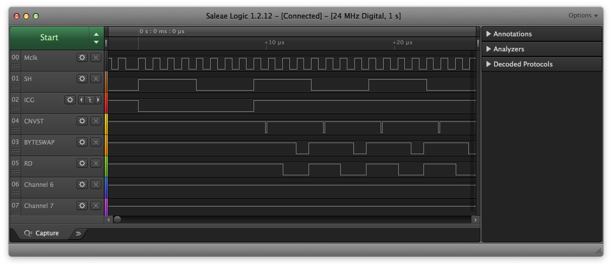
*UPDATE* Here is the .asc file for the LTC6417 op amp and also the logic analyzer screen capture for the MCLK for the TCD1304AP chip;
![]()
![]()
Above picture - TCD1304AP CCD chip (Toshiba)
Since I am using the AD8021 op amp as a unity - gain inverter to run the ADC (AD7667,) I needed to run a sim to check out some performance issues that Dave Allmon is having with the MAX232. Apparently it cannot keep up with the AD8021, so he has re-designed the entire schematic and added a new power supply.
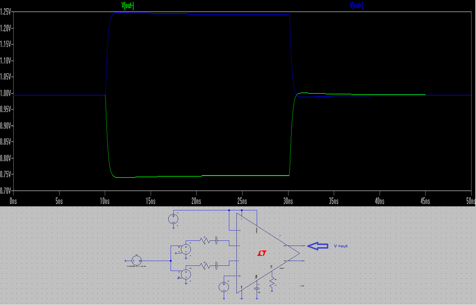
My mods will still work he said, but there may be an issue with the MAX232. I am going to upgrade to the MAX232EIN (16-pin dip,) now on LTspice there is no AD8021 op amp, even though I created one it doesn't work right, so I used their newest version which is comparable to the AD8021 and ran a sim test circuit.
My question is, at R4 I have variable resistor (2K,) to adust voltage at pin#3, it has to be 1.83v. When I run the sim on LTspice, I know I am using a different op amp with slightly different variables, but I am getting 1.25v out of what would be pin# 6 from the op amp?
![]()
Do you think I may be over driving the circuit (current wise,) with only a USB power source?
-
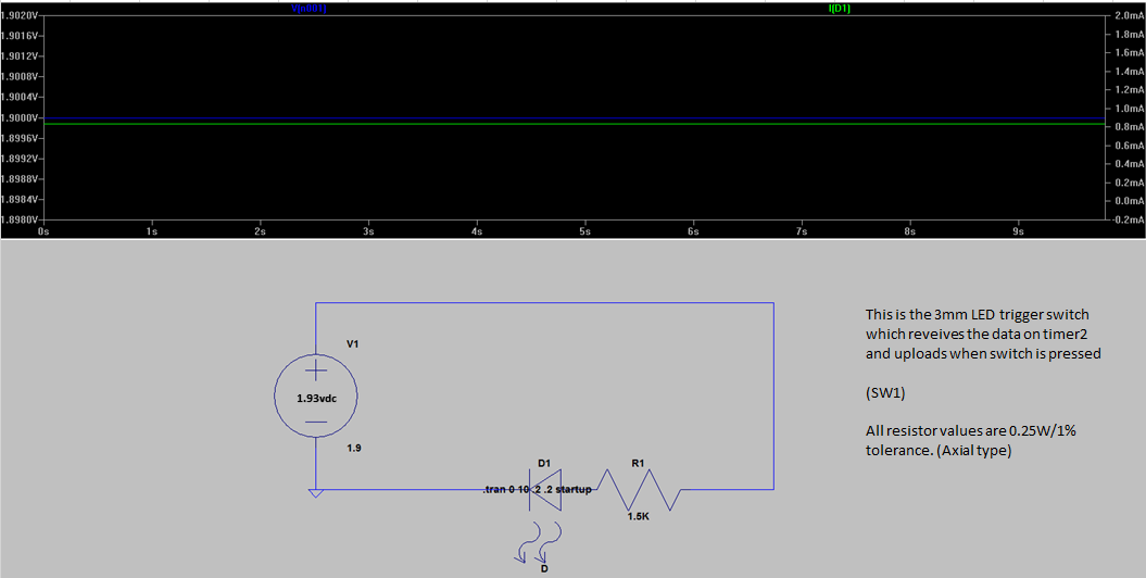
Fixed 3mm LED Indicator R-Value/LTspice SIM For CCD driver Circuit
02/27/2017 at 18:52 • 0 commentsI fixed the R value for the trigger switch at D2, for the CCD signal data upload when the 3mm LED lights up, I put a 1.5 ohm resistor and it brought the current to around 0.8mA (each port is 100mA so everything should be fine.)
![]()
-
Addendum To Log# 62 - Updated C/C++ code for TCD1304 CCD driver circuit
02/27/2017 at 00:13 • 0 comments#include <util/delay_basic.h>
#define RD (1<<2)
#define CNVST (1<<3)
#define BYTESWAP (1<<4)
#define ICG (1<<5)
#define SH (1<<6)
#define MCLK (1<<7)
// Full frame, including dark pixels
// and dead pixels.
#define PIXEL_COUNT 3694
#define CLOCKS PORTD
#define CLOCKP PIND
#define CLOCKS_DDR DDRD
#define DATA_PINS PINC
#define DATA_PORT PORTC
#define DATA_DDR DDRC
// 1mS exposure time.
#define EXPOSURE_TIME 10
// Initial clock state.
uint8_t clocks0 = (RD + CNVST + ICG);
// 16-bit pixel buffer
uint16_t pixBuf[PIXEL_COUNT];
char cmdBuffer[16];
int cmdIndex;
int exposureTime = EXPOSURE_TIME;
int cmdRecvd = 0;
/*
* readLine() Reads all pixels into a buffer.
*/
void readLine() {
// Get an 8-bit pointer to the 16-bit buffer.
uint8_t *buf = (uint8_t *) pixBuf;
int x = 0;
uint8_t scratch = 0;
// Disable interrupts or the timer will get us.
cli();
// Synchronize with MCLK and
// set ICG low and SH high.
scratch = CLOCKS;
scratch &= ~ICG;
scratch |= SH;
while(!(CLOCKP & MCLK));
while((CLOCKP & MCLK));
TCNT2 = 0;
_delay_loop_1(1);
__asm__("nop");
__asm__("nop");
__asm__("nop");
__asm__("nop");
__asm__("nop");
CLOCKS = scratch;
// Wait the remainder of 4uS @ 20MHz.
_delay_loop_1(22);
__asm__("nop");
__asm__("nop");
// Set SH low.
CLOCKS ^= SH;
// Wait the reaminder of 4uS.
_delay_loop_1(23);
// Start the readout loop at the first pixel.
CLOCKS |= (RD + CNVST + ICG + BYTESWAP + SH);
__asm__("nop");
do {
// Wait a minimum of 250nS for acquisition.
_delay_loop_1(2);
// Start the conversion.
CLOCKS &= ~CNVST;
CLOCKS |= CNVST;
// Wait a minimum of 1uS for conversion.
_delay_loop_1(6);
// Read the low byte of the result.
CLOCKS &= ~RD;
_delay_loop_1(3);
__asm__("nop");
__asm__("nop");
*buf++ = DATA_PINS;
// Setup and read the high byte.
CLOCKS &= ~(BYTESWAP);
_delay_loop_1(3);
__asm__("nop");
*buf++ = DATA_PINS;
// Set the clocks back to idle state
CLOCKS |= (RD + BYTESWAP);
// Toggle SH for the next pixel.
CLOCKS ^= SH;
} while (++x < PIXEL_COUNT);
sei();
}
/*
* clearLine() Clears the CCD.
*/
void clearLine() {
int x = 0;
// Set ICG low.
CLOCKS &= ~ICG;
CLOCKS |= SH;
_delay_loop_1(14);
// Set SH low.
CLOCKS ^= SH;
_delay_loop_1(10);
// Reset the timer so the edges line up.
TCNT2 = 0;
CLOCKS |= (RD + CNVST + ICG + BYTESWAP + MCLK);
do {
CLOCKS ^= SH;
_delay_loop_1(10);
} while (++x < PIXEL_COUNT);
}
/*
* sendLine() Send the line of pixels to the user.
*/
void sendLine() {
uint16_t x;
for (x = 0; x < PIXEL_COUNT; ++x) {
Serial.print(x);
Serial.print(",");
Serial.print(pixBuf[x]);
Serial.print("\n");
}
}
/*
* setup()
* Set the data port to input.
* Set the clock port to output.
* Start timer2 generating the Mclk signal
*/
void setup() {
CLOCKS_DDR = 0xff;
CLOCKS = clocks0;
DATA_DDR = 0x0;
Serial.begin(115200);
// Setup timer2 to generate a 667kHz frequency on D10
TCCR2A = (0 << COM2A1) | (1 << COM2A0) | (1 << WGM21) | (0 << WGM20);
TCCR2B = (0 << WGM22) | (1 << CS20);
OCR2A = 8;
TCNT2 = 0;
}
/*
* loop()
* Read the CCD continuously.
* Upload to user on switch press.
*/
void loop() {
int x;
char ch;
// If we got a command last time, execute it now.
if (cmdRecvd) {
if (cmdBuffer[0] == 'r') {
// Send the readout to the host.
sendLine();
} else if (cmdBuffer[0] == 'e') {
// Set the exposure time.
sscanf(cmdBuffer + 1, "%d", &exposureTime);
if (exposureTime > 1000) exposureTime = 1000;
if (exposureTime < 0) exposureTime = 0;
}
// Get ready for the next command.
memset(cmdBuffer, 0, sizeof(cmdBuffer));
cmdIndex = 0;
cmdRecvd = 0;
}
// Clear the CCD.
clearLine();
// Integrate.
delay(exposureTime);
// Read it for real.
readLine();
// See if the host is talking to us.
if (Serial.available()) {
ch = Serial.read();
// If char is linefeed, it is end of command.
if (ch == 0x0a) {
cmdBuffer[cmdIndex++] = '\0';
cmdRecvd = 1;
// Otherwise it is a command character.
} else {
cmdBuffer[cmdIndex++] = ch;
cmdRecvd = 0;
}
}
}
-
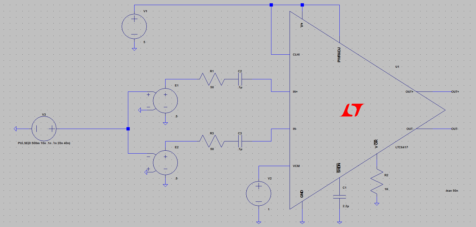
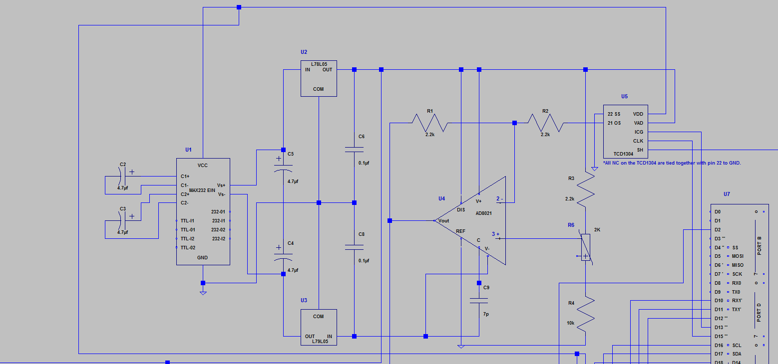
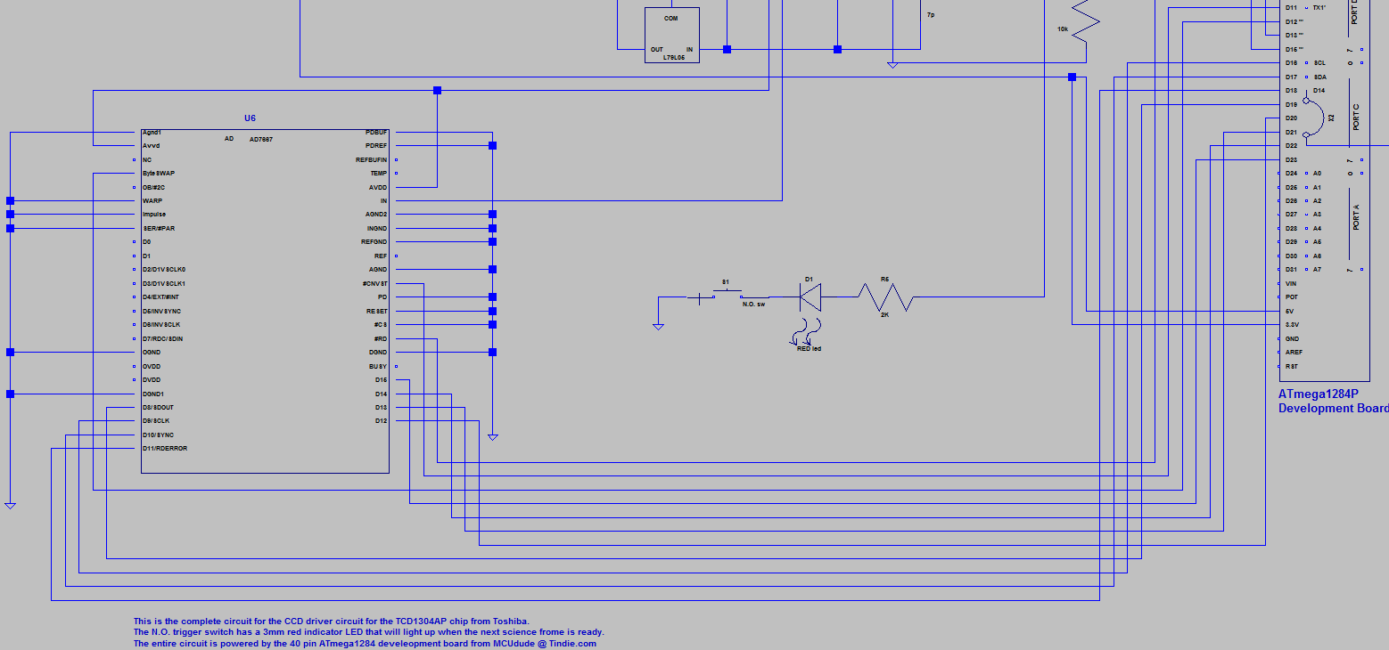
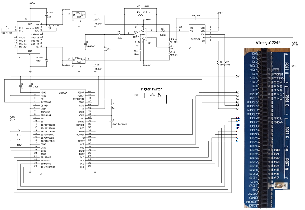
CCD Circuit Complete/TCD1304AP/LTspice schematic design
02/26/2017 at 18:54 • 0 commentsThis is a final draft of the CCD driver circuit before I assemble it next month, it is powered by the DIP-40 Arduino compatible development board (using the ATmega1284P-PU MCU chip.) The ADC (AD7667,) will be seated on a Schmartboard (40pin) The first block will be the drive components for the TCD1304 itself because this unit needs to be separate as it will be fitted within the spectrometer enclosure,
The ADC and MCU, will be designed as an interface unit (on its own proto board,) that can be connected to the CCD via serial port connector mounted on the side of the spectrometer.
The LTspice schematics are below are posted in 2 blocks, top and bottom (it was the only way I could make it fit, that was legible.)
![]()
![]()
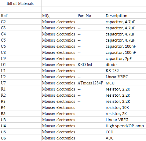
Below is the bill of materials;
![]()
-
*UPDATE: LTspice SIM/ Trigger Switch For CCD Driver Circuit/TCD1304AP
02/24/2017 at 14:58 • 4 commentsFirst part came in; The TCD1304AP CCD chip ! (received today Ebay $14.00)
![]()
I had to modify Dave Allmon's schematic for the trigger switch, he had a 1k res in series with the frame pulse for the next CTS. The LED I am using is a 3mm 40mA indicator, and 1k wasn't cuttin' it, so according to LTspice, the 3k resistor brings me right to the 100mA range, so I should be fine, if I'm wrong please feel free to correct me!
![]()
-
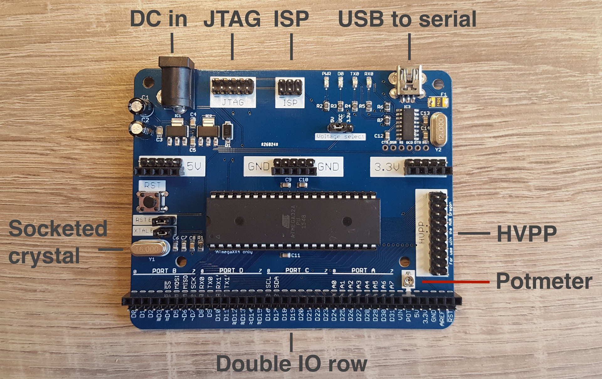
ATmega1284P/Schematic Design For The TCD1304 CCD chip
02/20/2017 at 14:51 • 4 comments*UPDATE: Go to the bottom of this page for code update*
This is the new re-worked design for the TCD1304 CCD driver circuit, I am utilizing a development board designed by MCDude over @Tindie http://www.tindie.com/products/MCUdude/dip-40-arduino-compatible-development-board/
This board will utilize the ATmega1284P (40pin) microcontroller, using an AD7667 as my ADC and a MAX232 and AD8021 driving the TCD1304, this will be a superior low noise and high efficiency circuit for the DAV5 V3 Raman spectrometer.
I am also in a somewhat collaborative effort with Dave Allmon since we are both using the same microcontroller (1284P,) just some tweaking in the code and this should be ready for testing in a couple of weeks.
![]()
Here is the development board;
![]() I'll also be using the FTDI FT232RL USB to serial IC from SparkFun;
I'll also be using the FTDI FT232RL USB to serial IC from SparkFun;![]() I removed the cleanline() part of the code, it was mean't to clean up any shot noise from the CCD, but it will also cause a blip to appear on your plot, so I took it out. Let your external processing software take care of that part. (this is in reference to my last log before this one where the "voodoo" line was included, Dave Allmon suggested to remove it, in cases where you are doing serious science, so I did.
I removed the cleanline() part of the code, it was mean't to clean up any shot noise from the CCD, but it will also cause a blip to appear on your plot, so I took it out. Let your external processing software take care of that part. (this is in reference to my last log before this one where the "voodoo" line was included, Dave Allmon suggested to remove it, in cases where you are doing serious science, so I did.Here is the new code;
#include <util/delay_basic.h>
#define RD (1<<0)
#define CS (1<<1)
#define CNVST (1<<2)
#define BYTESWAP (1<<3)
#define ICG (1<<4)
#define SH (1<<5)
#define MCLK (1<<6)
// Full frame, including dark pixels
// and dead pixels.
#define PIXEL_COUNT 3800
#define CLOCKS PORTF
#define CLOCKS_DDR DDRF
#define DATA_PINS PINK
#define DATA_PORT PORTK
#define DATA_DDR DDRK
// 10mS exposure time.
#define EXPOSURE_TIME 1
// Initial clock state.
uint8_t clocks0 = (RD + CS + CNVST + ICG);
// 16-bit pixel buffer
uint16_t pixBuf[PIXEL_COUNT];
/*
readLine() Reads all pixels into a buffer.
*/
void readLine()
{
// Get an 8-bit pointer to the 16-bit buffer.
uint8_t * buf = (uint8_t *)pixBuf;
int x;
cli();
CLOCKS |= (RD + CS + CNVST + ICG + BYTESWAP + SH);
OCR2A = 5;
TCNT2 = 0;
PORTB &= ~0x02;
for (x = 0; x < PIXEL_COUNT; ++x)
{
CLOCKS ^= SH;
CLOCKS &= ~CNVST;
CLOCKS |= CNVST;
_delay_loop_1(4);
__asm__("nop\n\t");
__asm__("nop\n\t");
__asm__("nop\n\t");
CLOCKS ^= SH;
CLOCKS &= ~(CS + RD);
*buf++ = DATA_PINS;
CLOCKS &= ~(BYTESWAP);
*buf++ = DATA_PINS;
CLOCKS |= (RD + CS + BYTESWAP);
}
sei();
}
/*
startLine() Toggles the clocks to shift the line
into the CCD shift register.
*/
void startLine()
{
// Set ICG low.
CLOCKS &= ~ICG;
_delay_loop_1(5);
// Set SH high.
CLOCKS |= SH;
_delay_loop_1(5); // 10uS.
// Set SH low.
CLOCKS &= ~SH;
_delay_loop_1(10);
// Set ICG high.
CLOCKS |= ICG;
}
/*
sendLine() Send the line of pixels to the user.
*/
void sendLine()
{
int x;
for (x = 0; x < PIXEL_COUNT; ++x)
{
Serial.println(pixBuf[x]);
}
}
/*
setup()
Set the data port to input.
Set the clock port to output.
Start timer2 generating the Mclk signal
Set the pullup on pin 2 for the start switch.
*/
void setup() {
CLOCKS_DDR = 0xff;
CLOCKS = clocks0;
DATA_DDR = 0x0;
Serial.begin(115200);
// Setup timer2 to generate a 1.333MHz frequency on D10
TCCR2A = (0 << COM2A1) | (1 << COM2A0) | (1 << WGM21) | (0 << WGM20);
TCCR2B = (0 << WGM22) | (1 << CS20);
// "5" causes 6 intervals - 0 through 5
OCR2A = 5;
TCNT2 = 0;
// Output Mclk on D2
DDRB |= 0x10;
// For the trigger switch.
pinMode(2, INPUT_PULLUP);
}
/*
loop()
Read the CCD continuously.
Upload to user on switch press.
*/
void loop() {
startLine();
readLine();
delay(EXPOSURE_TIME);
if (!digitalRead(2))
{
sendLine();
}
}
DAV5 V3.01 Raman Spectrometer
The only thing worth doing, is the thing worth doing right!


 I'll also be using the FTDI FT232RL USB to serial IC from SparkFun;