danjovic
-
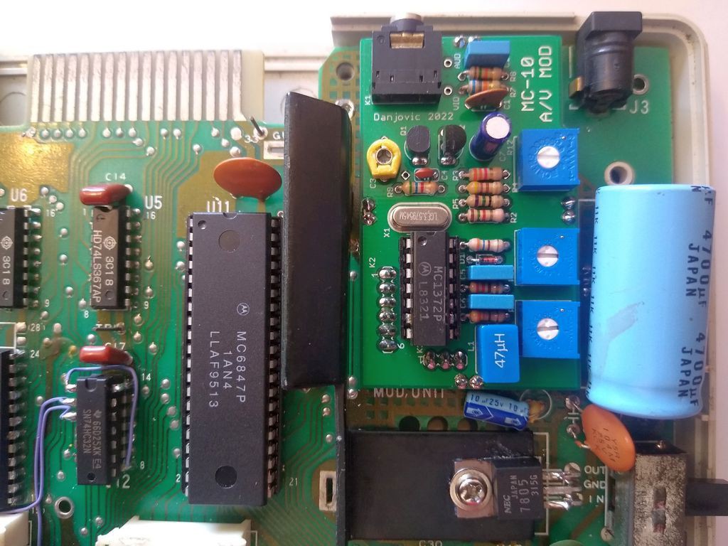
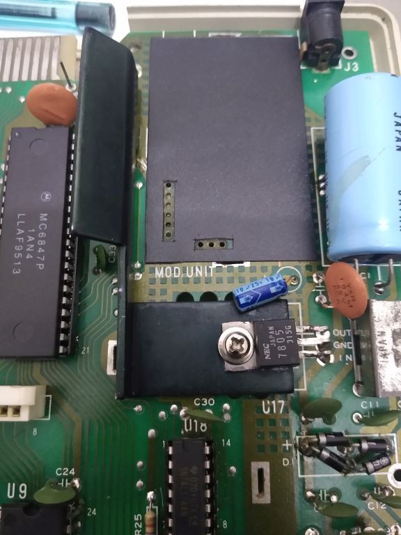
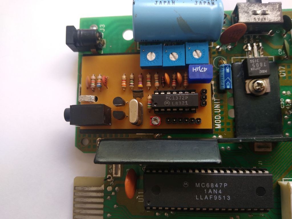
New PCB installed and adjusted
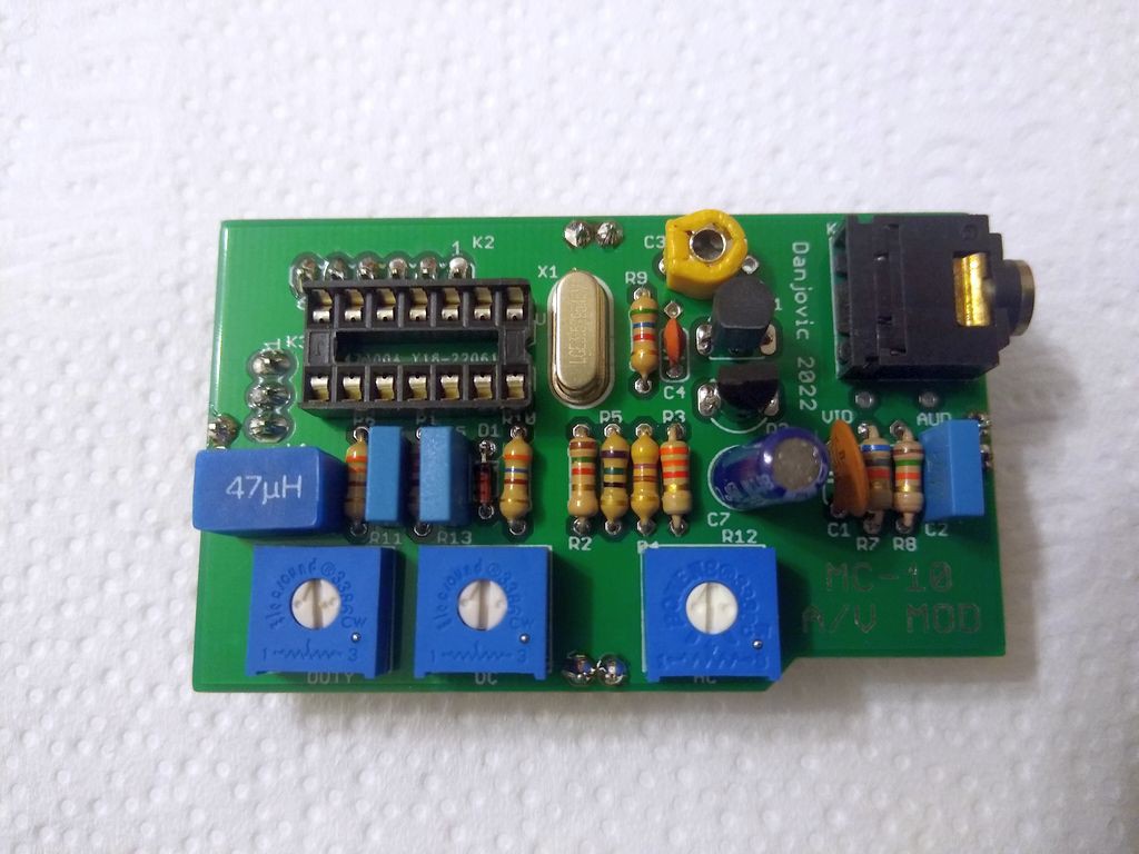
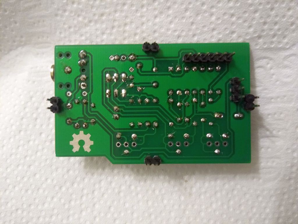
09/03/2022 at 17:15 • 2 commentsFinally found some spare time to install and adjust the new board.
![]()
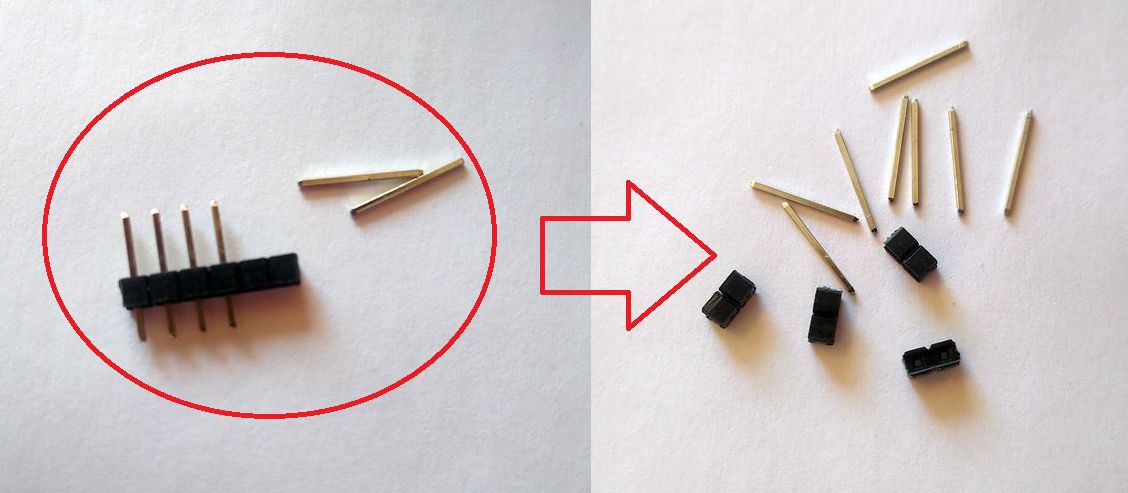
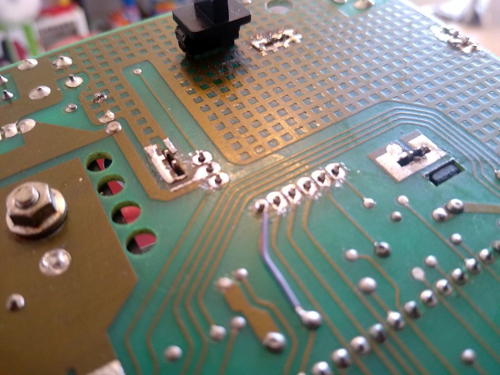
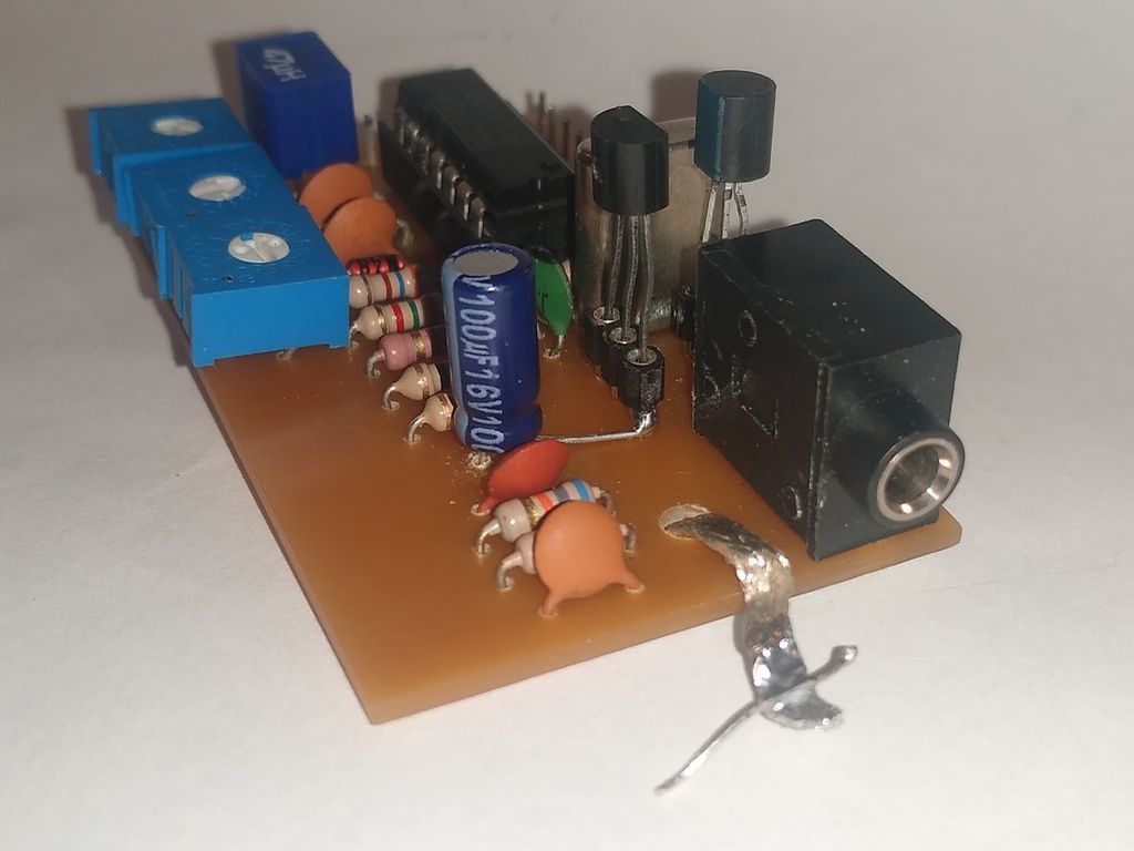
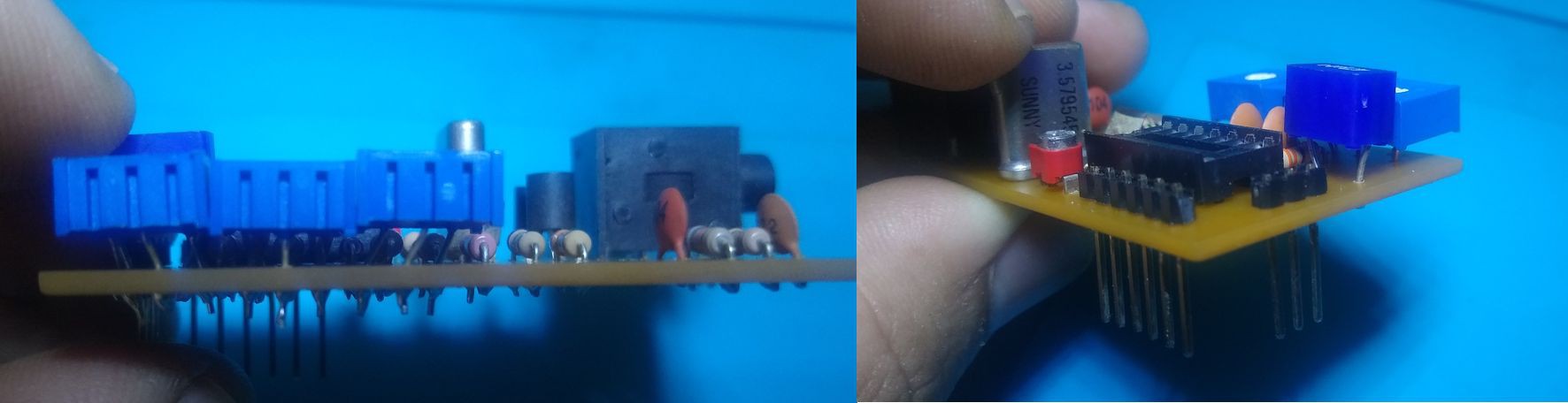
First thing I have noticed is that the height of the pin header spacers were not enough to provide clearance for the P2 jack.
![]()
To workaround that I have removed the spacers from other pin headers and stacked them on the top of the existing ones
![]()
![]()
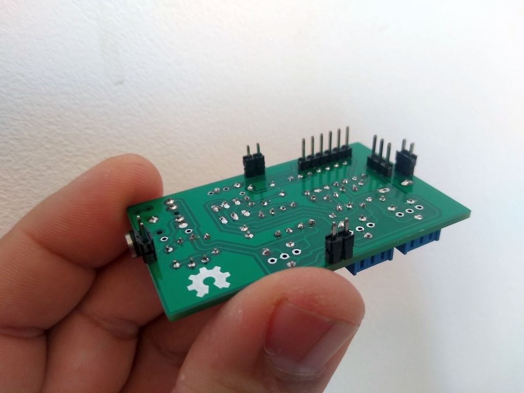
The remaining length of the pins was enough to pass through the board and solder them in place
![]()
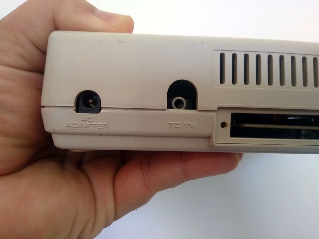
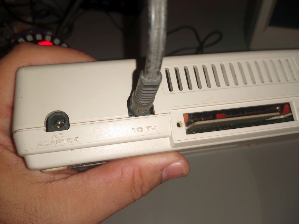
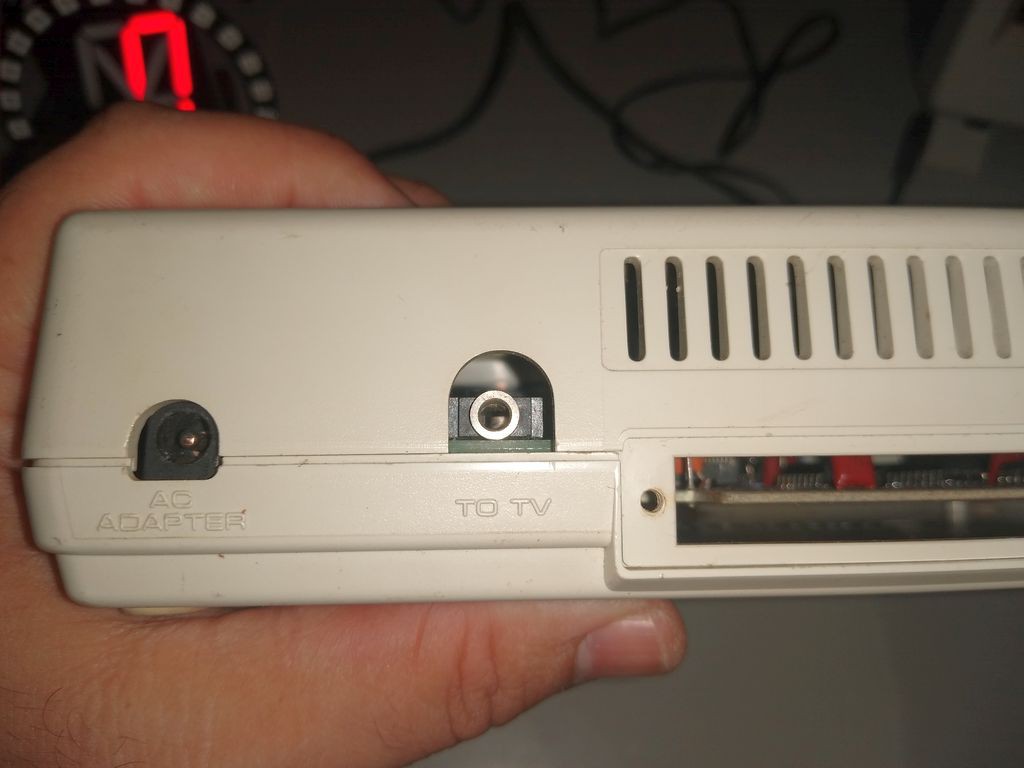
After that there was clearance enough to insert the P2 plug.
![]()
![]()
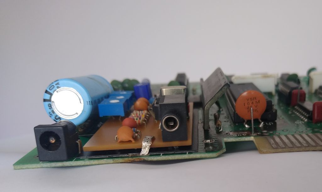
Nevertheless I should design another board using the original P2 jack, and enhance the centering of the output jack.
![]()
Adjustments
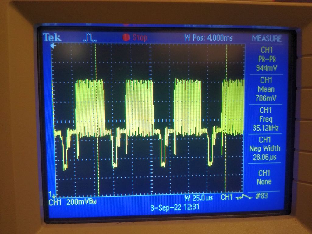
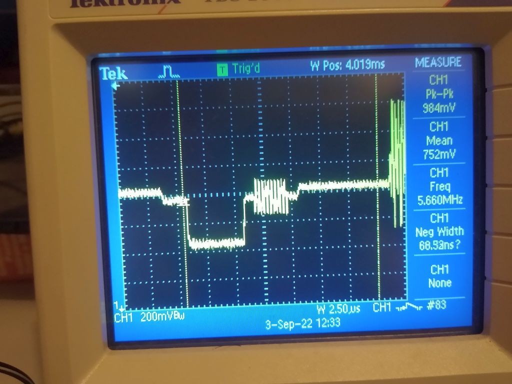
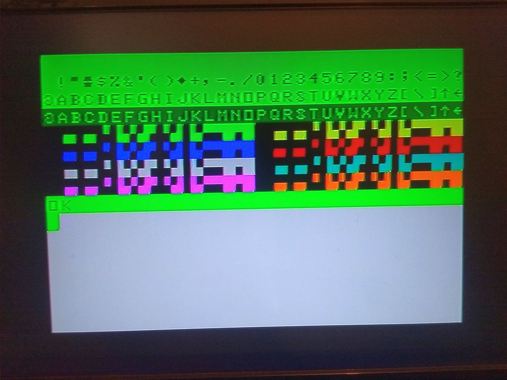
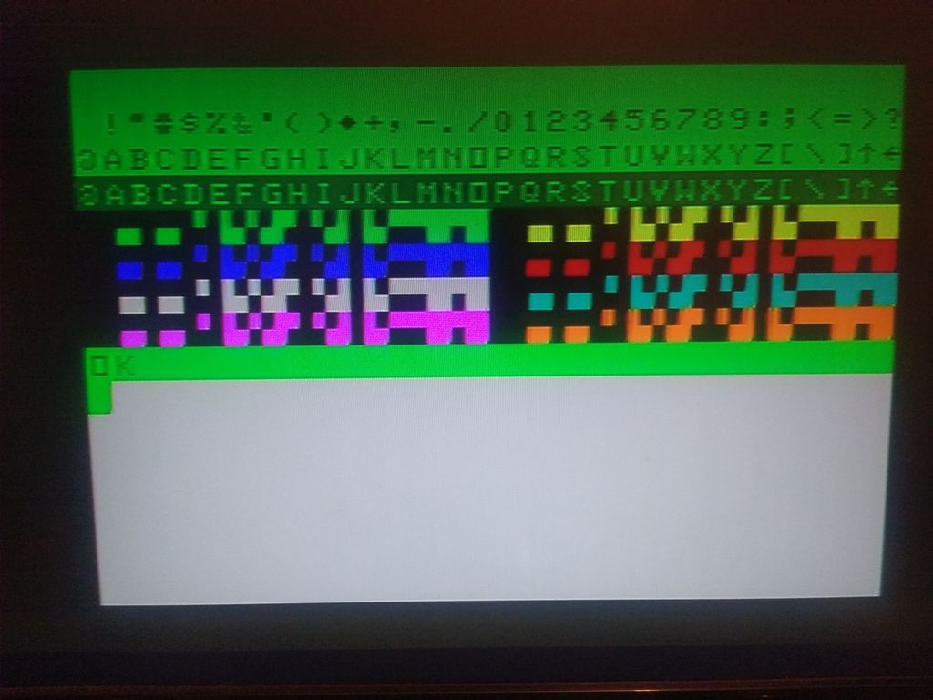
The adjustments went normal, as with the other board. I have used a program to produce all possible colors on the screen
10 CLS 5 20 FOR F = 0 TO 255 30 PRINT CHR$(F); 40 NEXT F- DUTY adjustment adjusts the amplitude of the color component in the signal, but the effect of the adjustment is marginal, at least on my LCD TV.
- AC amplitude should be adjusted to get close to 1Vpp with the video output loaded (connected to TV )
- DC amplitude should be adjusted to bring the BIAS DC level of the video signal the most close to zero. It is not possible to get the bottom of the pedestal at 0 Volts (let alone the black level). Nevertheless adjust the DC trimpot to the point where the sync tip starts to shrink
![]()
![]()
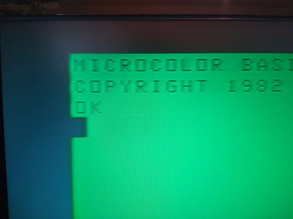
Results
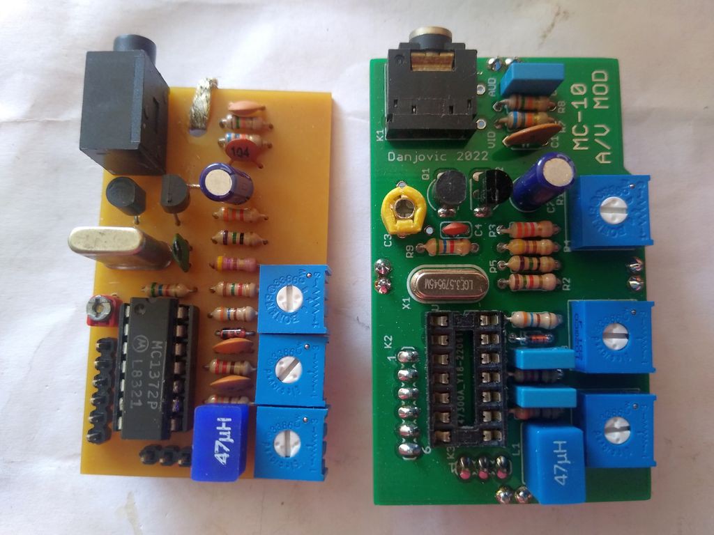
The resulting image is nice, just like with the previous version of the board (which is just like expected as the schematics are the same.
![]()
-
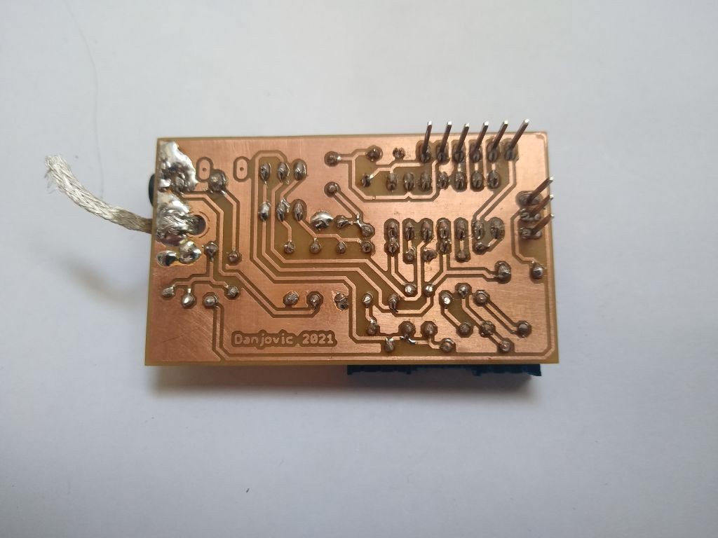
New PCB assembled
08/11/2022 at 01:59 • 1 commentAll components fits nicely.
![]()
![]()
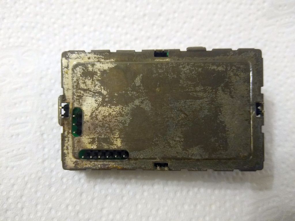
Checking the alignment of the mounting pins with the RF modulator can. It looks good
![]()
Next opportunity I will assemble the board on the MC-10 and perform the adjustment.
-
Brand new PCB
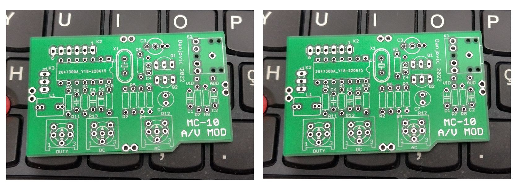
08/01/2022 at 15:11 • 0 commentsI have just received the new PCB.
![]()
-
Alternative Board
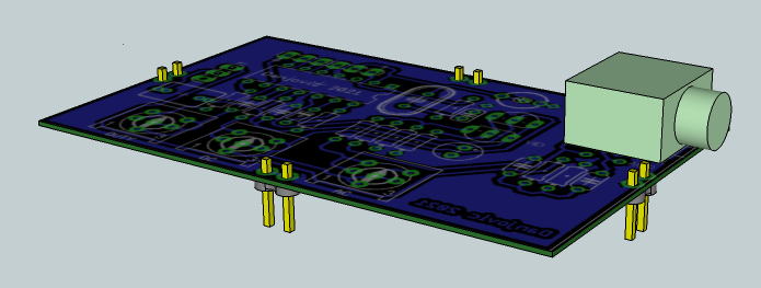
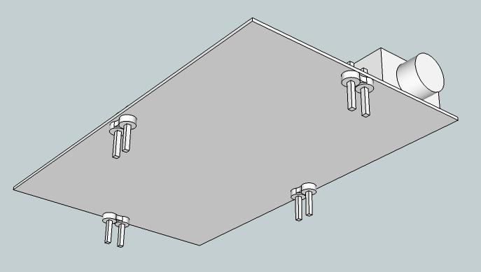
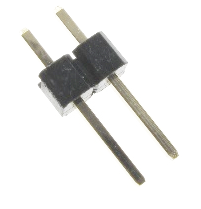
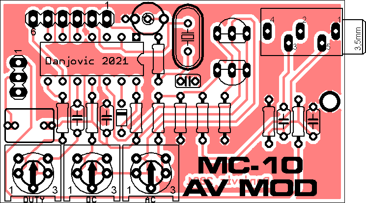
12/10/2021 at 02:18 • 0 commentsWorking on a study for an alternative board, using a slightly larger PCB with a 1x2 pin headers at the middle of each edge of the board matching with the holes for the modulator shield.
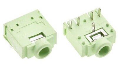
The output connector should be changed to a PJ307 with a lower profile to compensate the extra height of the headers (compared to the previous version of the board)
![]()
![]()
Board Layout. It was necessary to move some components and it looks like the lower right corner may need some relief to not interfere withe the power input jack.
![]()
PJ307
![]()
Pin Header 1x2
![]()
-
Wrapping up
11/28/2021 at 13:16 • 0 commentsI have added a capacitor to the prototype. I used a 100uF / 16V part because of its diameter (the 47uF part used in debugging was too thick and I ran out of 10uF on my parts bin). The negative terminal was inserted on a hole made with a 0.8 drill bit right above the ground plane but there was no room for the hole of the positive terminal, that ended being soldered on the transistor socket.
![]()
The most recent version of the PCB provides the holes for the bypass capacitor (C7).
![]()
Now I was able to adjust the video signal to an acceptable quality. There is no instructions for this adjustments available on the MC1372 nor on the MC6847 datasheet.
Then I have used the DC offset and AC gain potentiometers to have the video with similar proportions as the NTSC standard. I think I should dig a little more on that, but so far I have the colors with the hues expected (to may eyes).
![]()
I removed the transistor sockets and soldered the prototype board on its place.
![]()
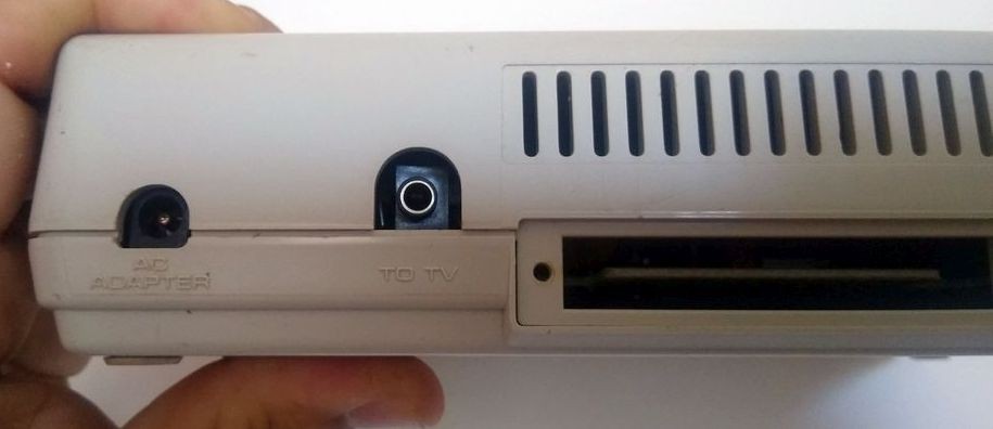
After closing the case the P2 socket was perfectly aligned with the plastic case
![]()
-
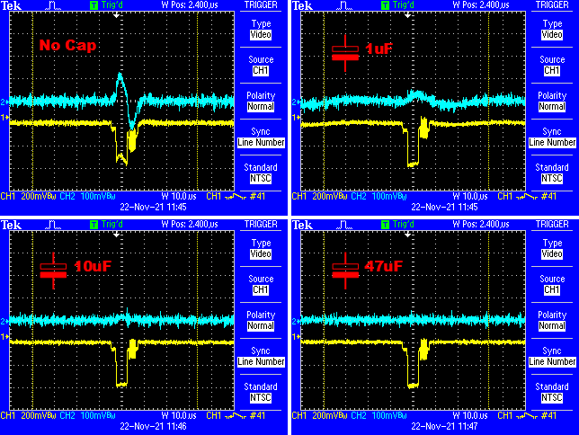
Experimenting with the Bypass Capacitor
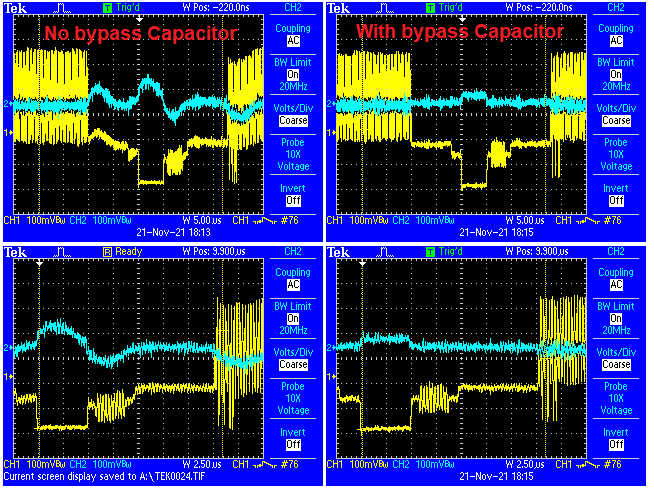
11/22/2021 at 16:09 • 0 commentsI have experimented with some values for the bypass capacitors. Anything above 10uF should work fine. The blue trace was taken at the capacitor of the PNP transistor (the circuit's VCC) and the yellow trace is the video output, acquired on an empty line to be able to see the ripple along the whole line.
![]()
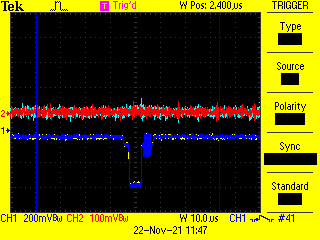
Any value above 10uF should do. Below is the overlap of voltage waveform using a 47uf (in Red) over the 10uF (in blue). Not much difference.
![]()
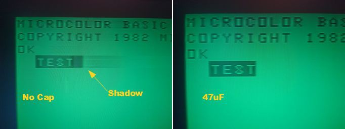
And the image below shows the shadow caused by the ripple of the Vcc voltage.
![]()
-
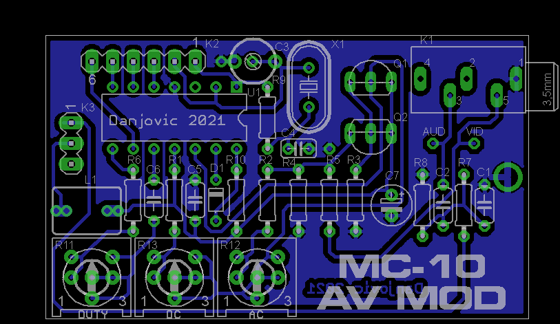
PCB Updated
11/22/2021 at 04:40 • 0 commentsI have just updated the PCB:
- Added the 47uF bypass capacitor on Vcc
- Added two testpoints for the output video and audio signals
- Added a third footprint option for the trimpot (3296W)
- Added extra pad for the crystal load capacitor C4 to compensate differences in footprint
- Added extra pads for the Inductor to compensate differences in footprint
- Aligned the hole for the GND braid with the hole of the modulator shield on the motherboard
![]()
-
Tests, adjustments
11/21/2021 at 20:31 • 0 commentsThe MC-10 PCB received a piece of auto-adhesive poly-carbonate from a leftover sign to isolate the AV/Board from the motherboard.
![]()
Two rows of SIL headers have been soldered to the A/V board
![]()
And the board was mounted on the MC-10.![]()
The first run looked ok!
![]()
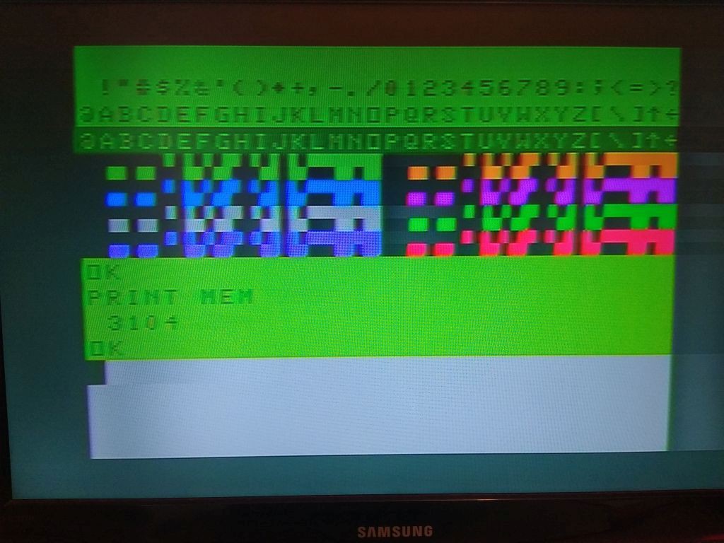
But running a program to test the characters showed that the colors did not looked as expected,
![]()
At least the memory now shows the expected amount of (3102 bytes) due to the OR logic provided by the extra 74LS32.
After some experiments with the trimpots, I still didn't have the right colours showing up (btw the screen can be cleaned by CLS[1-8] command.
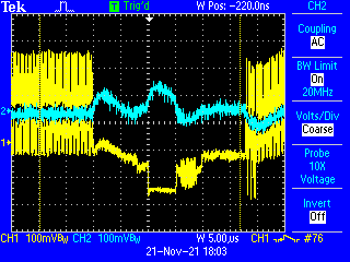
I checked the waveform of the video signal and it presented some distortions.
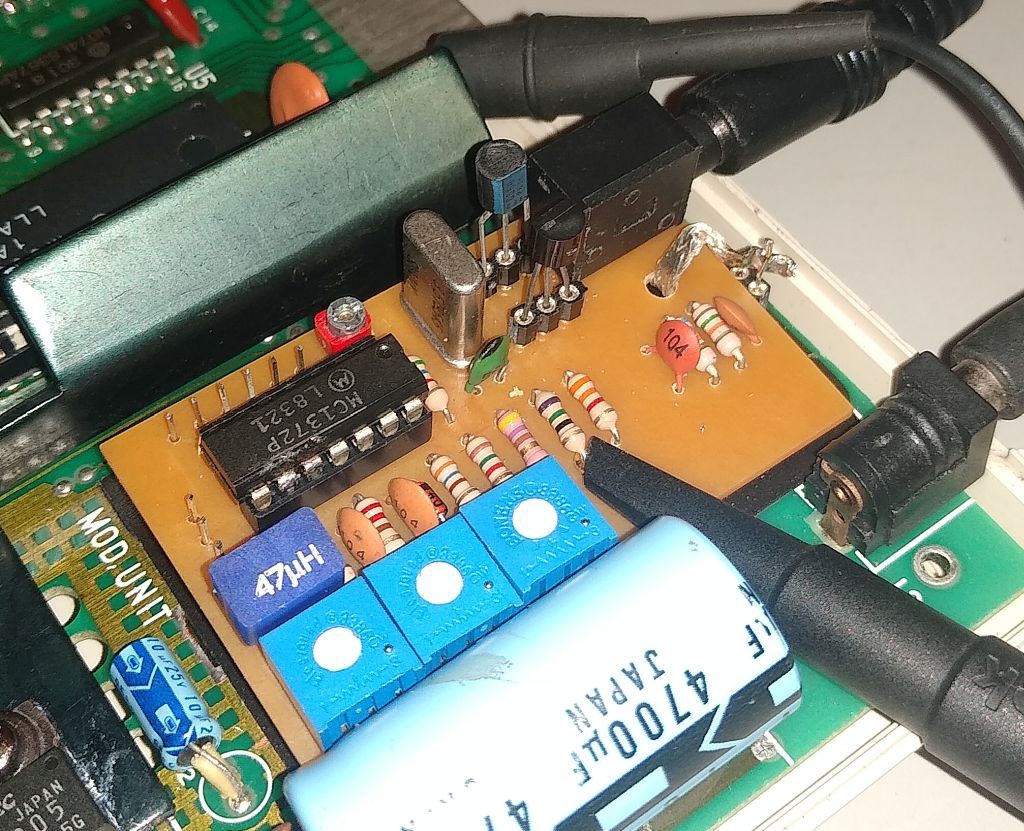
Suspecting of the transistors I have used, I took the board out and istalled some sil sockets to allow ease replacement of the transistors.
![]()
I have experimented with a bunch of transistors from my parts bin, both NPN and PNP from series BC2xx, BC3xx and BC5xx and noticed that :
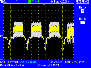
The "first" transistor (PNP) makes the most difference. At the end the PNP transistors that best performed were the BC55x series, being the BC556 the one that provided the greatest output amplitude for a same position of the potentiometers.
The picture below shows the difference between the BC328 (in yelllow) and a BC560 (in white)
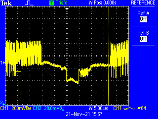
At the end I was able to adjust the colors to an acceptable hue, but did not get rid of the distortion on the signal, easily noticed on the sync region.
Then I measured the waveform at the output of the MC1372 (the base of the PNP transistor) and found a fluctuation on the voltage with exactly the same profile of the distortion on the waveform.
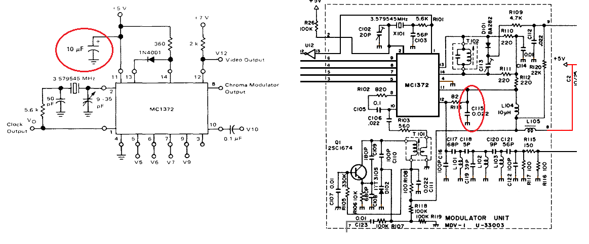
Checking the schematics again, I have noticed that the original circuit uses solely a 22nf power supply bypass capacitor alas the schematics from the MC1372 datasheet have a 10uF capacitor.![]()
Then I took a random electrolytic from my parts bin, a 47uF and attached it between pins 4 and 11 and voilà! The nasty ripple disappeared.
![]()
I will update the schematics to include the capacitor.
-
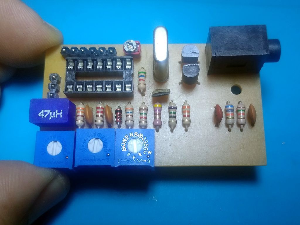
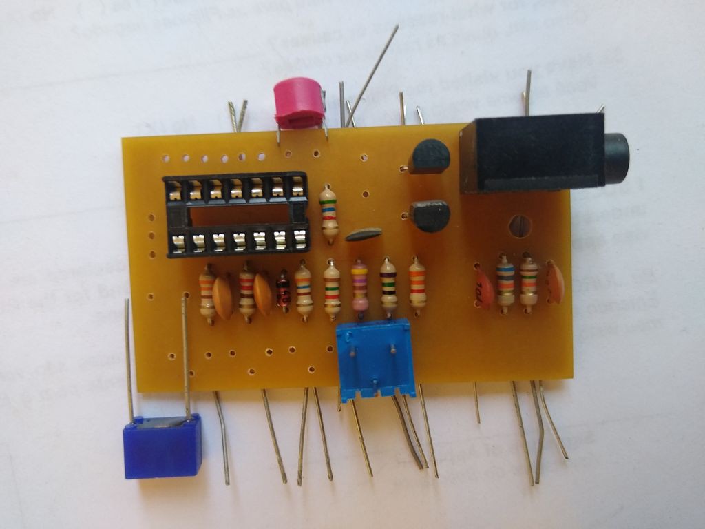
Prototype Assembled
11/13/2021 at 01:45 • 0 commentsJust finished to assemble the prototype of the A/V board.
![]()
I was able to reuse the trimmer from the original modulator board, but it was necessary to bend the leads of the inductor and the trim-pots
![]()
I have already updated the board layout to accommodate the alternate footprints for the trim pot, the inductor and also the trimmer. I should print the board on paper to do a tryout before uploading the sources to github
![]()
It was not possible to have an alternate jack. I should release 2 more versions for alternate types of 3.5mm jacks.
-
Alternative footprints
11/12/2021 at 16:05 • 0 commentsThe trimpots, the trimmer and the inductor have their footprints slightly different from the my libraries, but they were the ones I could find for purchase.
![]()
I usually wait for all components in hand before etch a prototype board but I could not afford more time to order them again and wait for the delivery, so I will bend the terminals and proceed to the testing/adjustments.
On the other hand I will update the PCB to accept some alternative footprints for this components, an probably add an alternative for the 3.5mm jack.
MC-10 A/V mod Board
Use composite Video instead of RF in your Tandy Micro Color Computer