-
[A] New LCD background image and renders
07/17/2023 at 06:56 • 0 commentsSource of background: https://wallpaperscraft.com/wallpaper/fractal_shapes_glow_235436
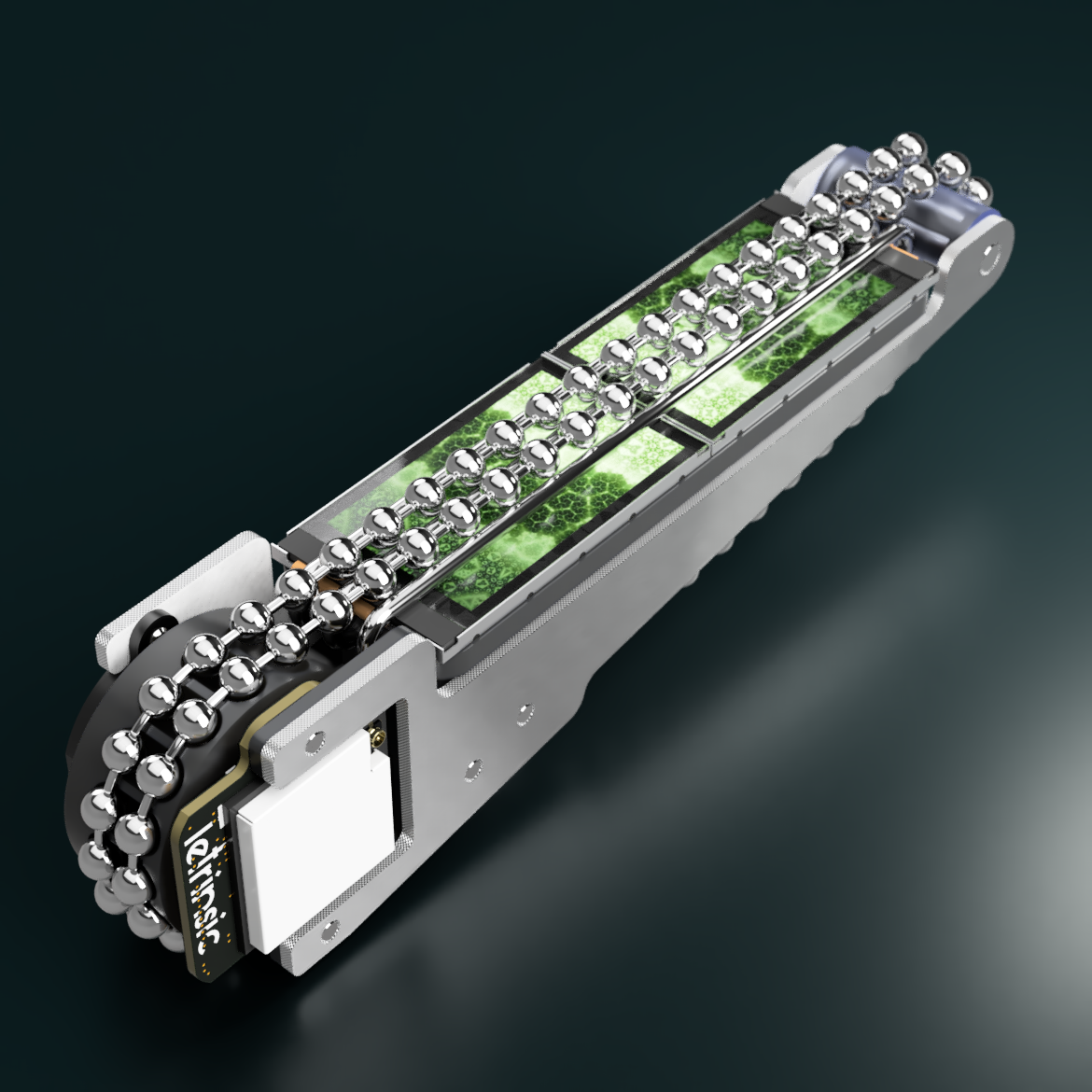
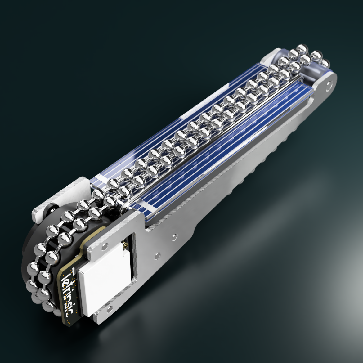
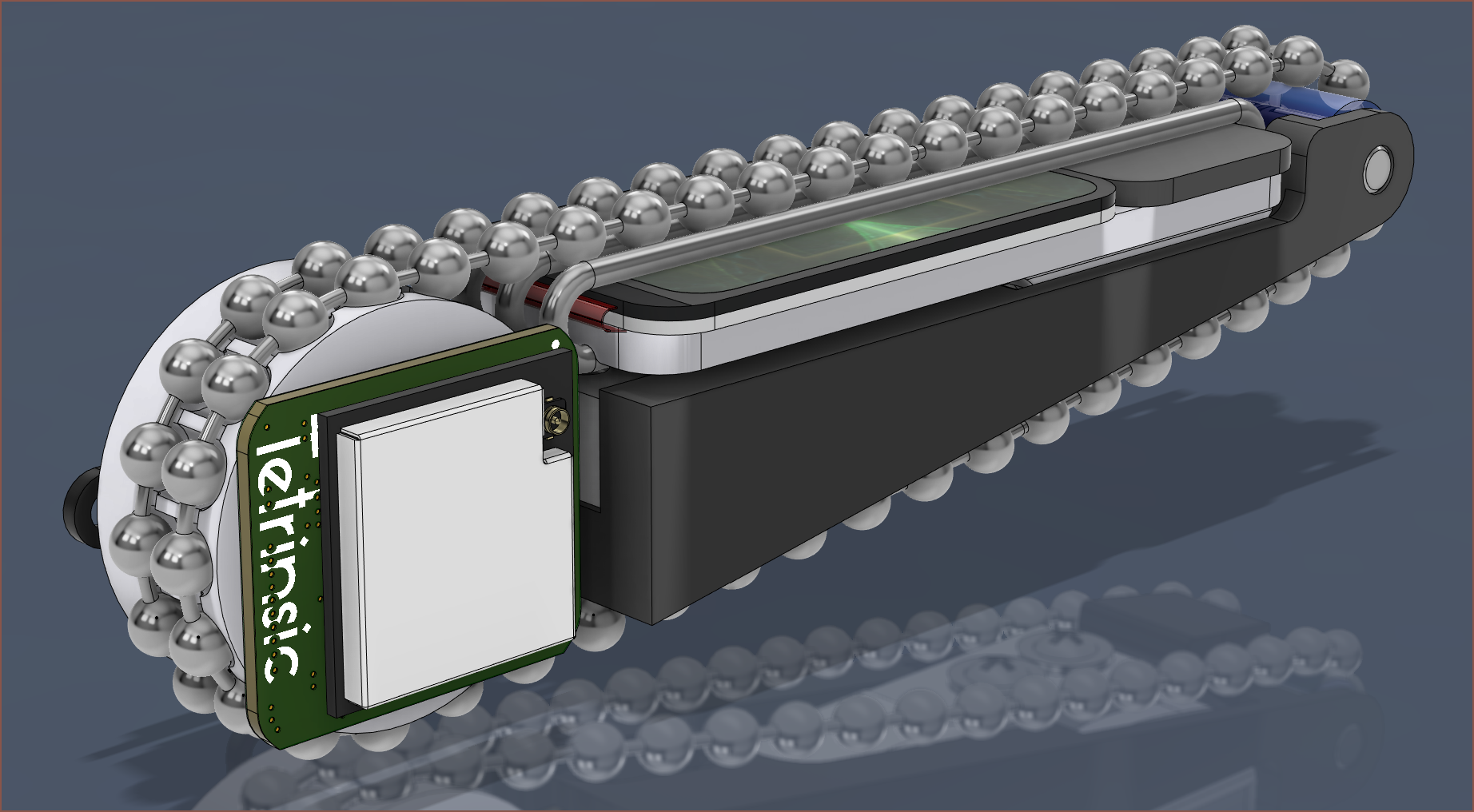
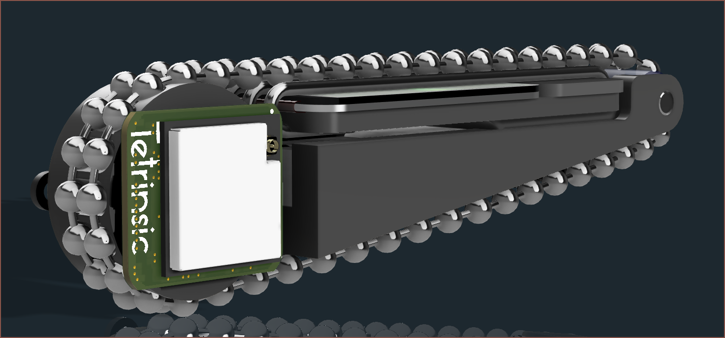
Hue changed by 240 degreesI'm finally closing in to a similar completed state as the very first Tetrinsic concept, hardware-wise. I thought it would be a good idea to commemorate the relatively radical redesign of Tetrinsic from a dual path, single LCD solution to a dual LCD, single path one by finding a new background (see below).
Unfortunately for me, it seems that this entire process has taken 3 hours -- 2 for choosing / editing an image and 1 for setting up the render. Part of the 1hr setting up the render was to do with setting up slightly more accurate textures of the plates, such as the white soldermask or rough milled textures of the edges.
It's also interesting to know that I'm now at save v359. Only the #SecSavr Skyrise [gd0092] has more saves (v385) and that's an entire FDM printer. I guess it's to be expected, since digital input devices are used by billions and so all the low-hanging fruit of faster input methods have likely all been found already.
Tetrinsic Taic looks really cool and every past version of myself in the last 15 or so years (whenever the Horizon Fuel Cell H2Go RC Car came out) would be happy to know that a futuristic input device may very well be powered by renewable energy.
This log took 50 minutes to create. -
[M] Frame connector and pressure plate pusher
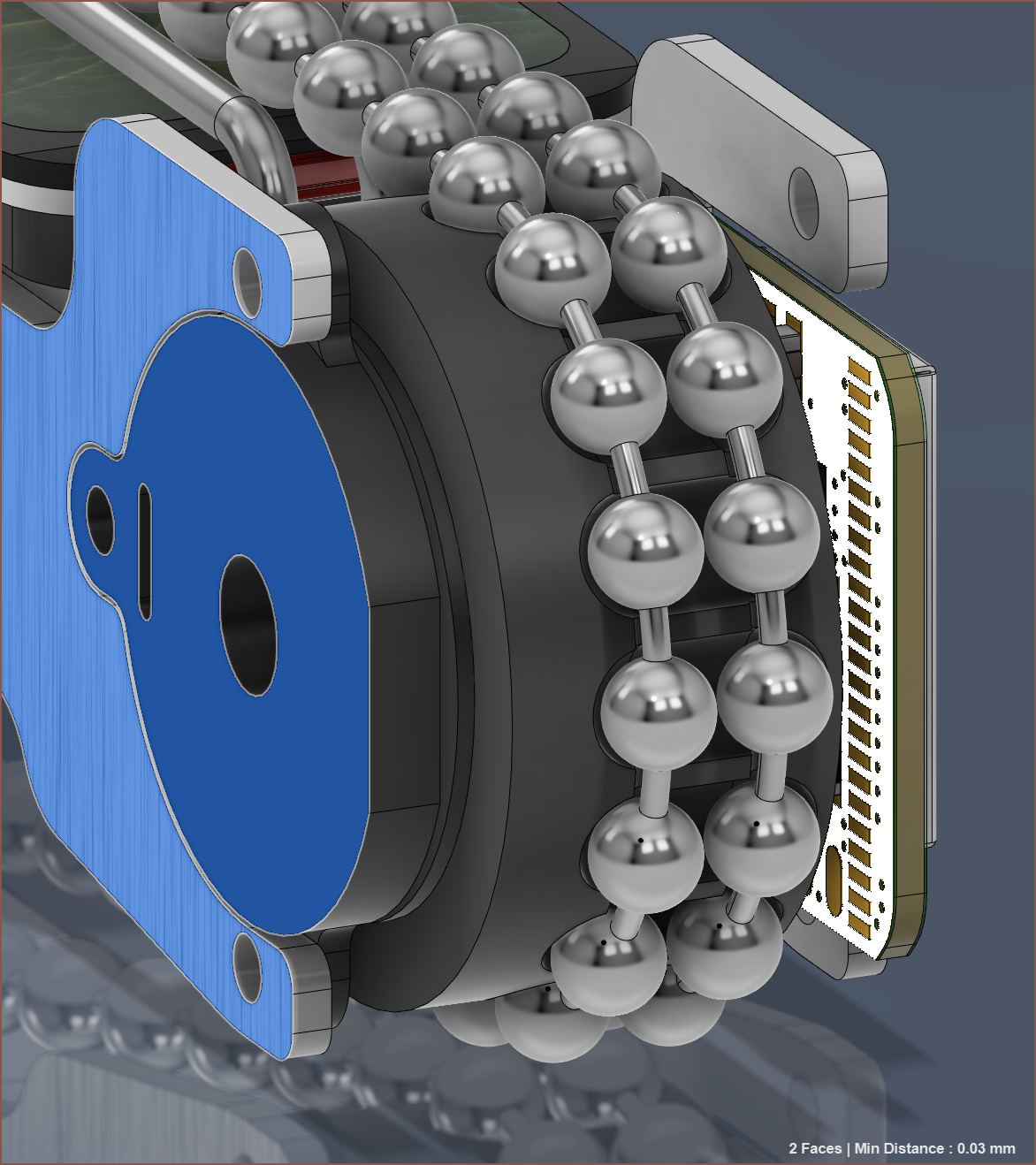
07/17/2023 at 03:24 • 0 commentsI've now modelled the 3d print that connect the two frame plates together, as well as modified the pressure plate to push the ball-chain around the load cell.
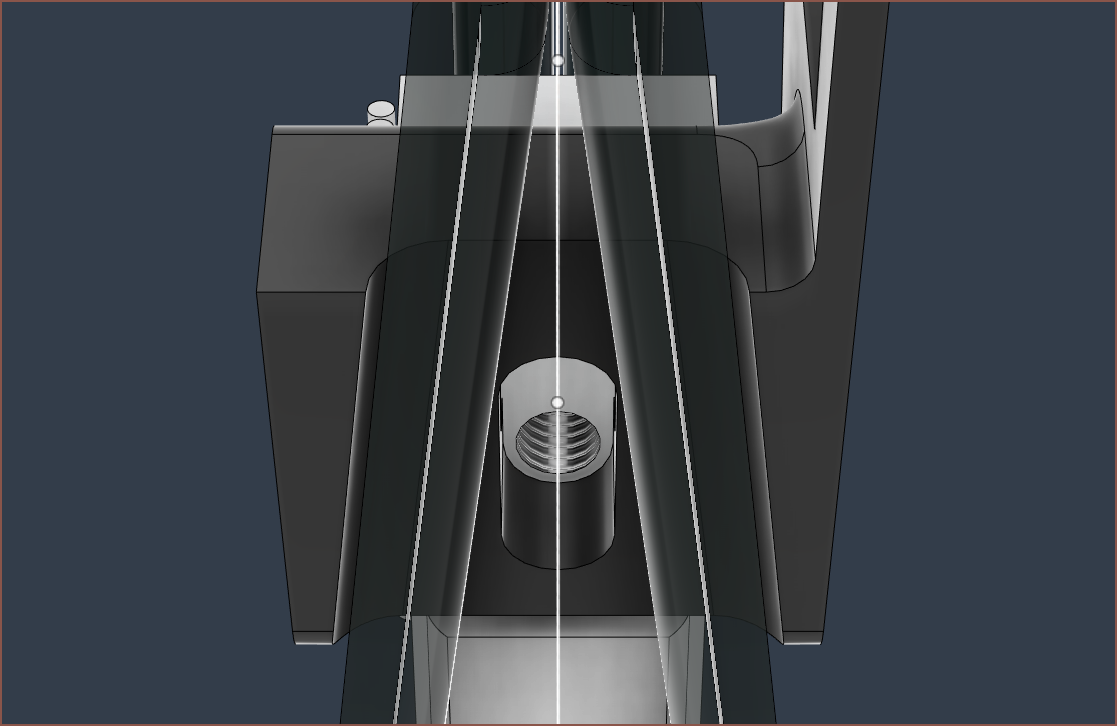
The plan is to use 2mm dowels as locating pins and then glue the frame plates together. The frame connector also acts as a spacer for the PCB. For mounting Tetrinsic to something, the frame acts like a massive spacer between the load cell and attachment surface. To put it another way, the M3 bolts go through the mounting surface, then the frame connector (narrowly missing the ball-chain path) and finally screw into the tapped holes of the load cell.
Hopefully, the tension of the ball-chain keeps the load cell + pressure plate assembly somewhat fixed in place during assembly.
-
[R][T] 1.56" AMOLED and LCD backlighting
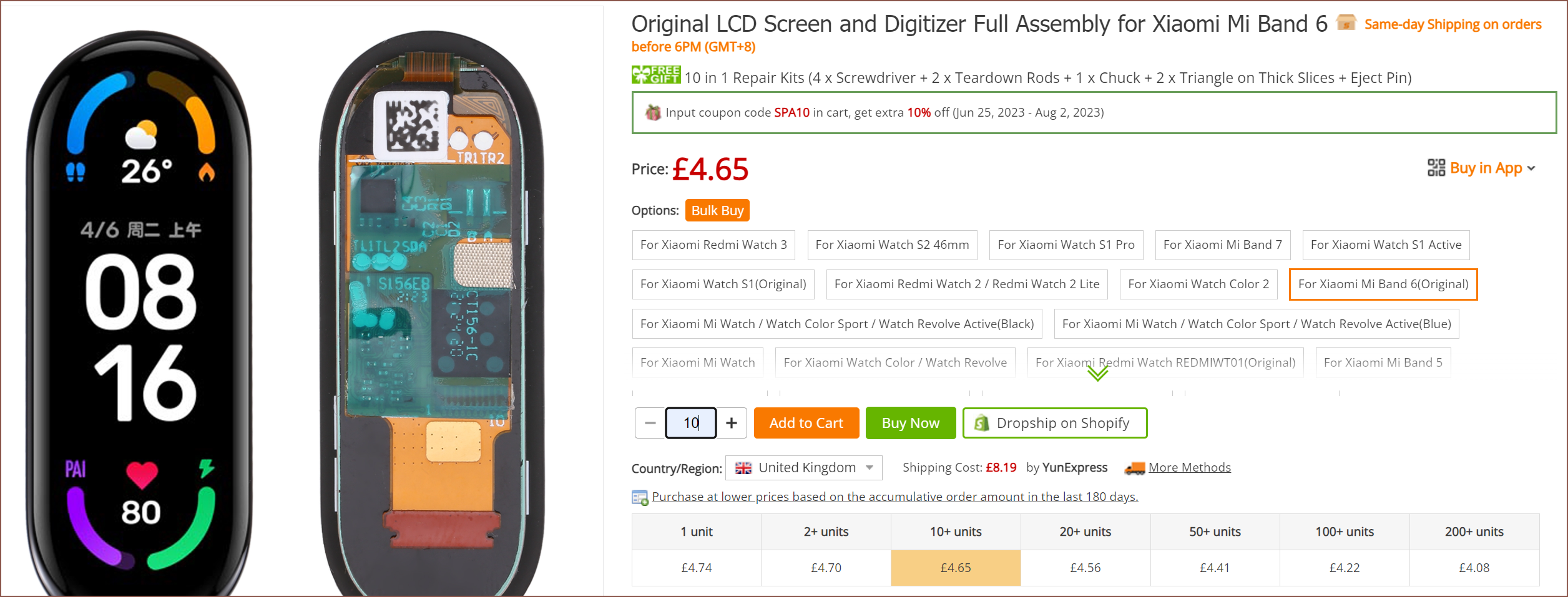
07/16/2023 at 04:41 • 0 commentsBefore I stopped researching once and for all, I had a look on Panelook for the largest screen that's less than 18mm wide. I found the TA016XVHM05 which is an SPI AMOLED panel that's 45mm in length (which means that I could have a 3d printed circle extension, as 45 + 18 = 63). I can't seem to find this anywhere, nor what it even looks like. There's also a MIPI panel (TA016XVHN05) that has 31 pins, and it seems that it's used in the Xiaomi Mi Band 6. SUNSKY has the lowest price where I've found the panel, which also comes with front glass for that extra premium look.
With shipping, it's £5.10/display for 10pcs, or 55% more expensive than dual 1.14" screens.
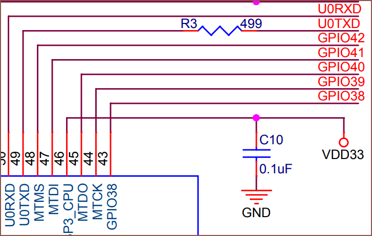
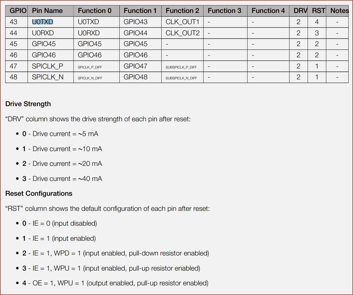
Speaking of those LCDs, I'm going to have to tap into the unused UART pins:
The good news is that these pins are right next to where the current display CS and backlight pins are. I was wondering if I should just drive both backlights with just one pin, but considering that each screen is likely to have brightness variances and that if I'm using one of the UART pins, I might as well use the other one too, I then decided to see if I could somehow fit the circuitry for 2 backlight drivers.
Well, as it turns out, there's only 1 LED in the 1.14" LCD and it only needs 20mA! IIRC, the 1.47" LCD required 180mA.
Digging into the ESP32-S3 datasheet, the current output of each pin is actually adjustable! In the MINI datasheet, it says that 40mA can be sourced and 28mA can be sunk from a GPIO.
The real question is if I can use those UART pins at all. Looking at the MINI schematic, it already looks like I can only use RX for backlighting since TX has an almost-500 ohm resistor on it.
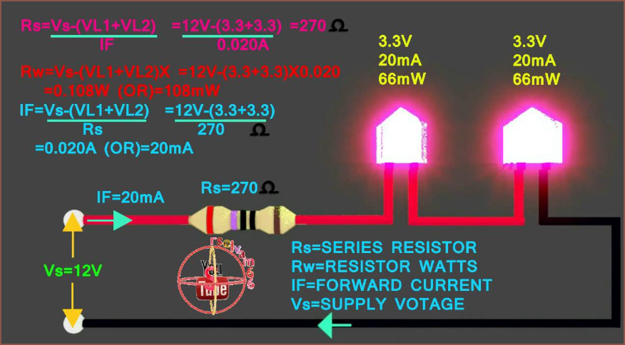
Using the below equation I found on the internet, I believe I need a 15 ohm resistor between the pin and the LED anode. Alternatively, I could always just have a maximum PWM value such that the pin maxes out at 3.0V. There's likely going to be a voltage drop anyway too.
It also seems that, unlike most other pins that have reset configurations of input enabled/disabled, TX sounds like outputting a logic 1 and both have a 45kOhm pull up enabled. Looking at the LCD docs, it sounds like this is fine as it only listens on the SPI bus when the CS pin is a logic 0:
I've also looked at how it's been done on the T-Display, which is an ESP32 (not ESP32-S3) development board with a 1.14" display, and they've done the traditional transistor circuit. I guess, worst case scenario, such circuitry is added onto the pressure plate PCB that the LCDs actually connect to, since there's more space there.
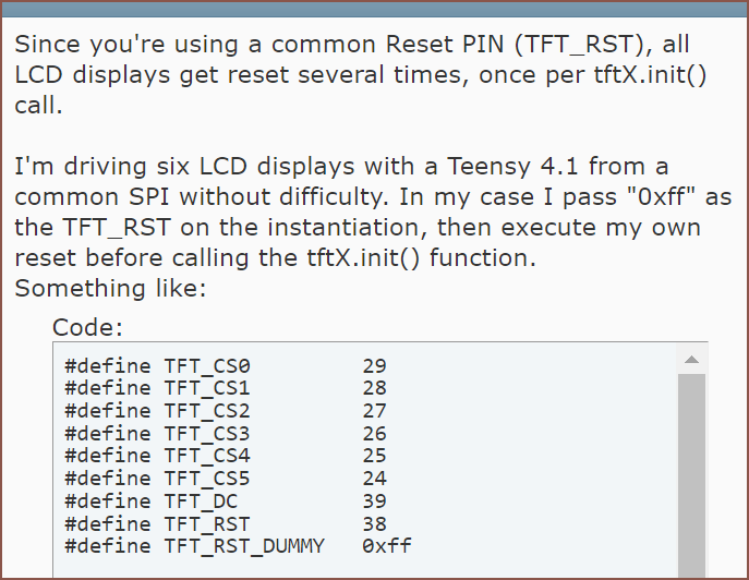
I also checked to make sure that I could use multiple LCDs on the same reset pin, and I can if I code in a dummy pin, as seen below.
In other news, I've added the same tabs as the BLDC onto the PCB. If you've seen #Coaxial Hotend [gd0144] logs, the shape may seem familiar.
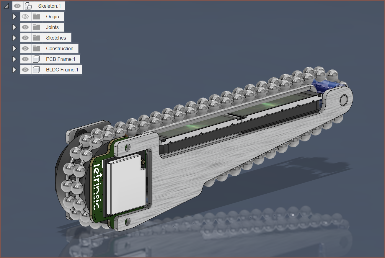
Next, I've started recreating the skeleton:
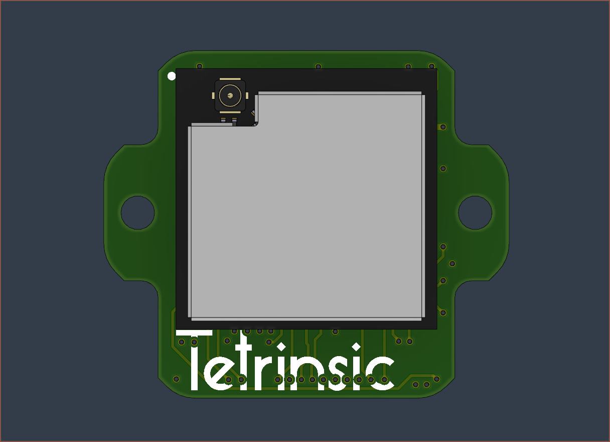
The frame cuts are 91mm, and it seems that the price break at JLCPCB is 100x100mm. I'll need to find out how big the antenna connector is so that I can ensure that I'd be able to connect it. Right now, I'm assuming that I'd be able to use the copper layer to solder the two together with brass tubing, but if not I'll just swap it so that the silkscreen is visible instead.
This log also took 110 minutes to create.
-
[M][R] Applying tweaks from Tetent Concept
07/13/2023 at 20:55 • 0 commentsThe concept print: https://hackaday.io/project/184181-tetent-gd0090/log/221171-p-concept-half-print
Essentially, I'm going to have to mandate that 18mm thickness I just so happened to acheive when switching to this 3.2mm ball chain solution. I've also got to aim for a slope angle of 18 degrees.
Solar Cell
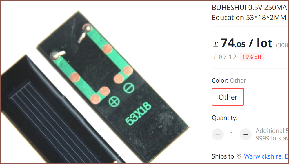
First, I wanted to research on my off-the-shelf solar panel options. I have a feeling that I could always cut down a larger panel if I get the process right, but off-the-shelf reduces manufacturing requirements on an already multi-fabrication design (wire bending, 3D printing, PCBA, aluminium milling).
First thing I saw was this:
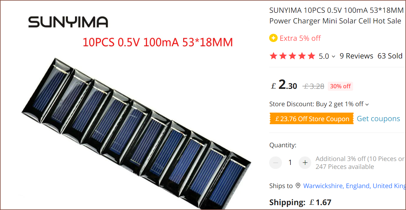
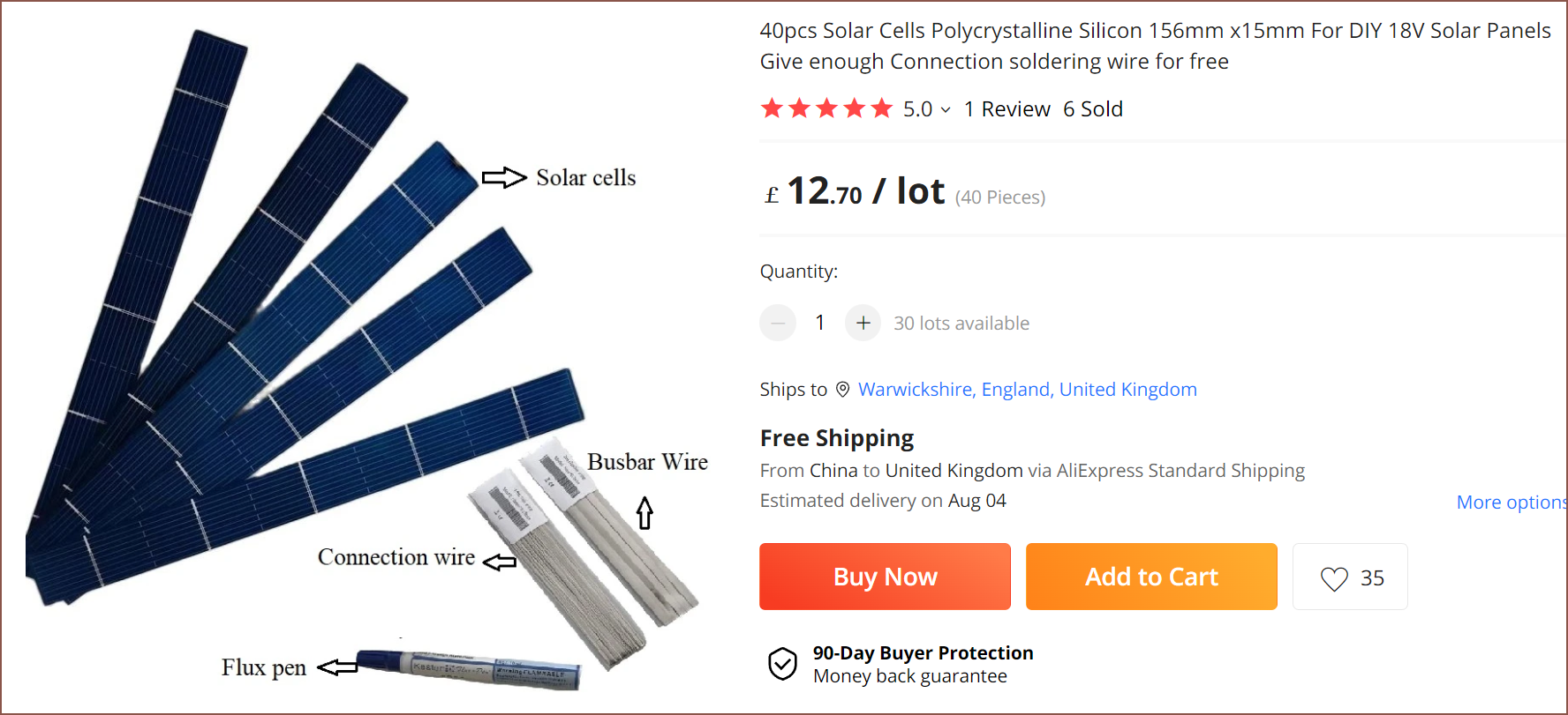
Something felt kind of... off, since I probably would've been fine with this already if I got 0.25A from one. It turns out that most of them are understandably only 0.1A:
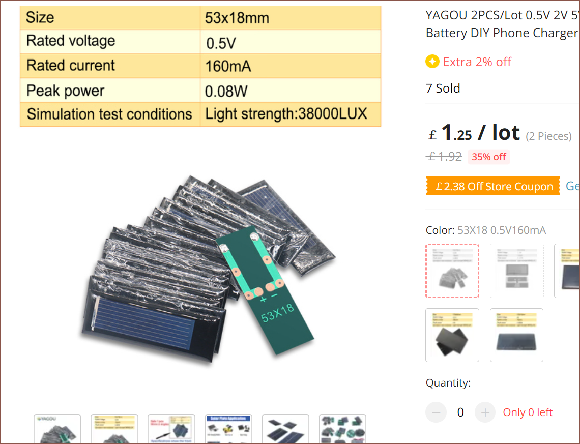
I was able to find one that produced 0.16A, and it visibly has more solar panel area inside:
Oh wait. I just found the below video. It's super easy -- barely an inconvinience -- to cut a cell:
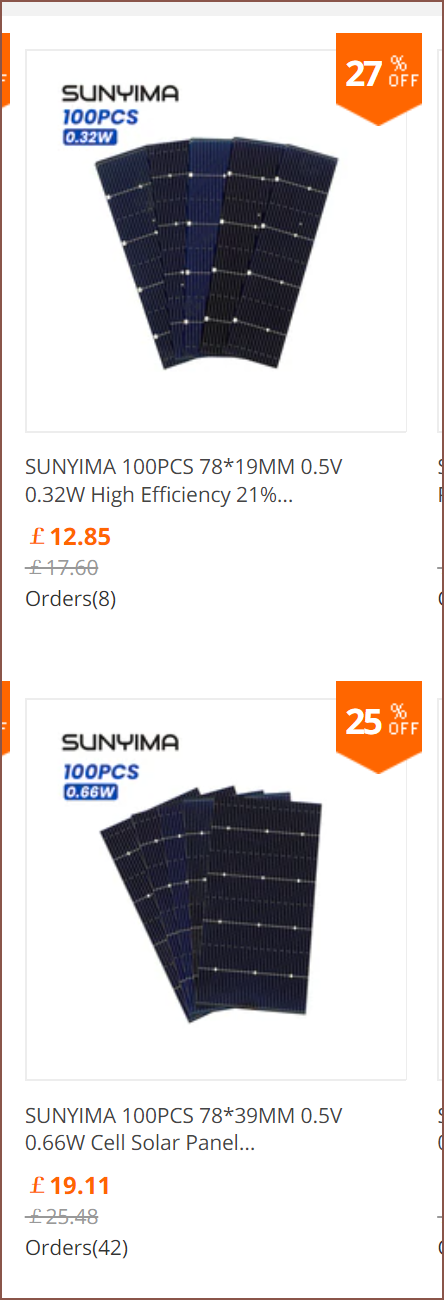
That means "reality can be whatever I want". The cheapest, highest efficiency cell that I can cut to size would be the 78x19mm cell I found earlier on, but it's more efficient from a cost and manufacturing standpoint to cut 2 panels at once from a 78x39mm cell:
There's also a seller that has a 15mm wide kit:
Modelling
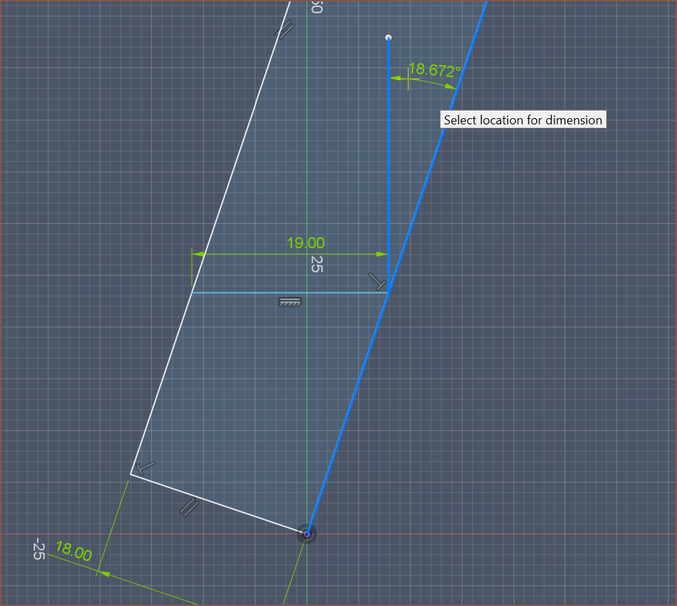
Sometihng interesting to know is that, if spaced precisely 18mm apart, I'd achieve a 18-ish degree "stagger" with a horizontal spacing of 19mm:
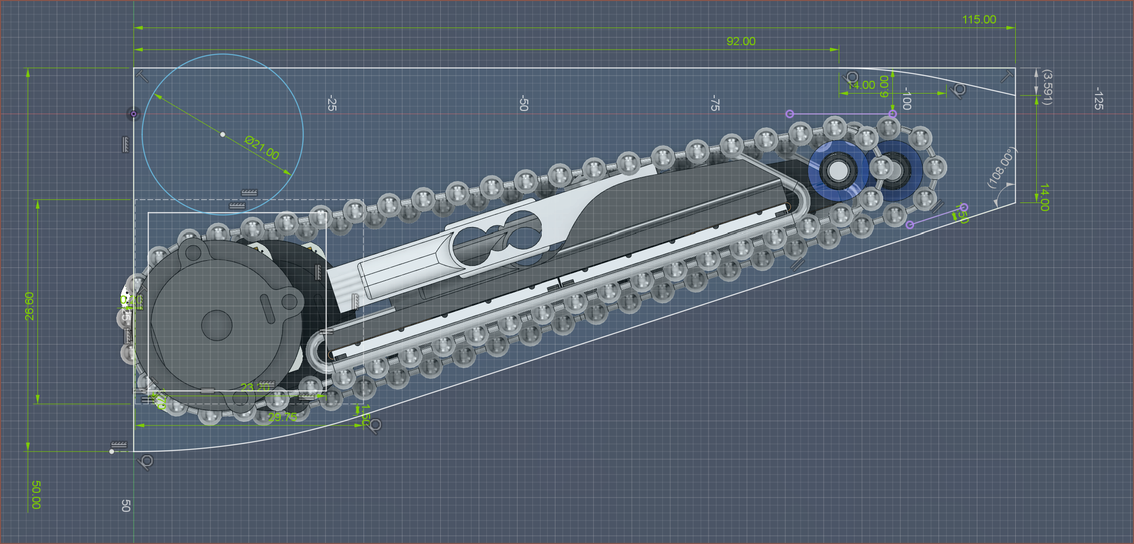
Anyway, the new design is a rather long 104mm:
That, along with the steeper angle, makes for some issues downstream:
-
[T][M] Aluminium PCB Skeleton?
07/12/2023 at 23:52 • 0 commentsThe idea I had was to generate a freeform model of the skeleton (see last log) and then see if it could be adapted to use JLCPCBs aluminium PCB service which comes in thicknesses of 1.0mm, 1.2mm and 1.6mm. As it turns out, the distance between the bottom of the motor and it's mysterious tabs is 1.17mm so I can use the 1.2mm option:
I'm not exactly sure what the motor tabs are for, but I'm going to try and use them with 2mm dowels. This would also be what I use to position the PCB. I'm also imagining printed parts with dowels to position them and lastly glue the whole thing together. Due to space constraints, there's not really any space to use bolts.
In unrelated news, I seemingly accidentally made the new component outside of the Tetrinsic component.
Yes, sure, I can and have just moved it in but I'm very tempted to just remake it. I need to tweak how I've done the skeleton anyway, since it'll still be much cheaper. I still haven't fully figured out how I'm mounting Tetrinsic to Tetent.
-
[T][M] SLS 3D Printed Skeleton?
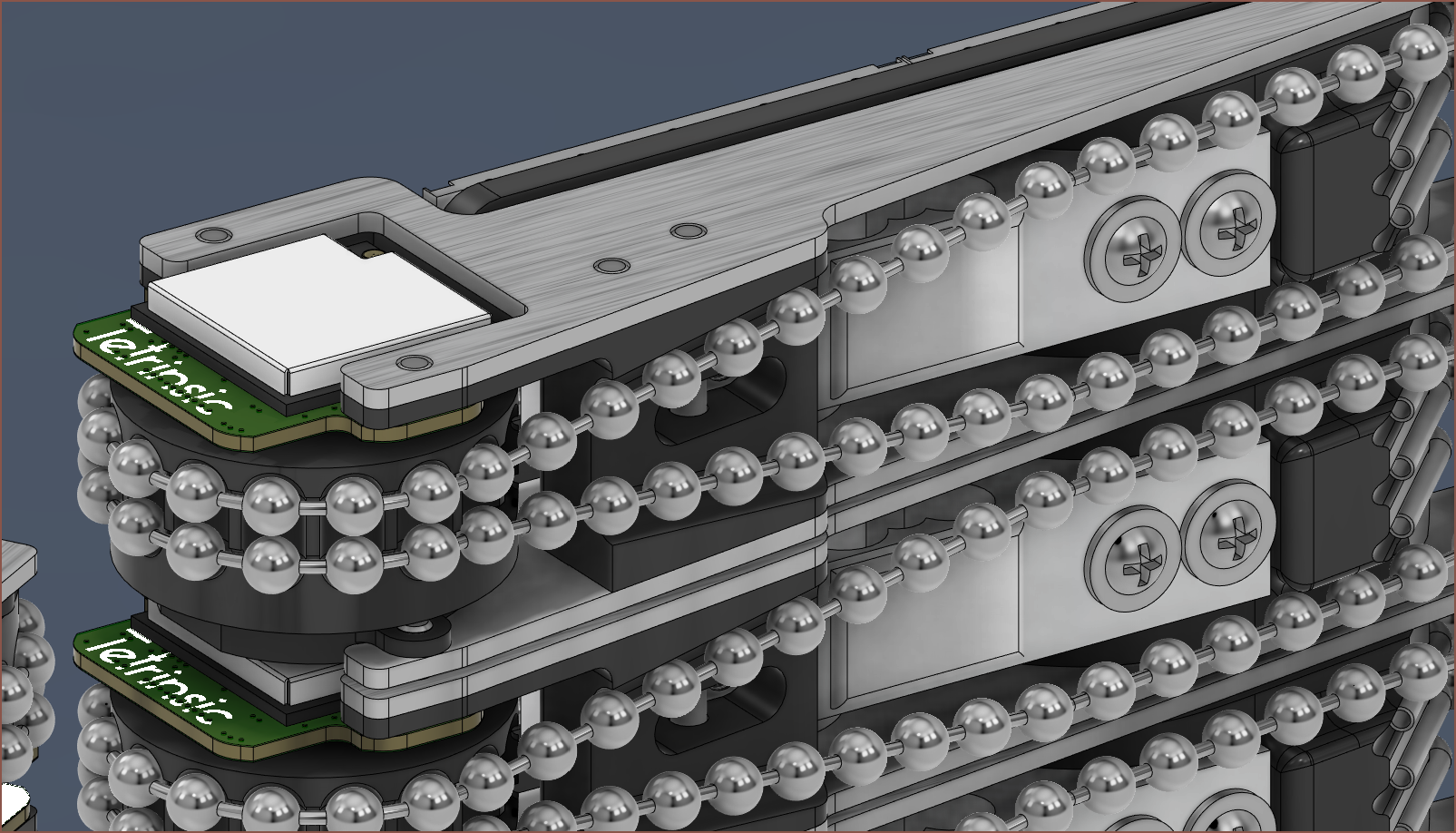
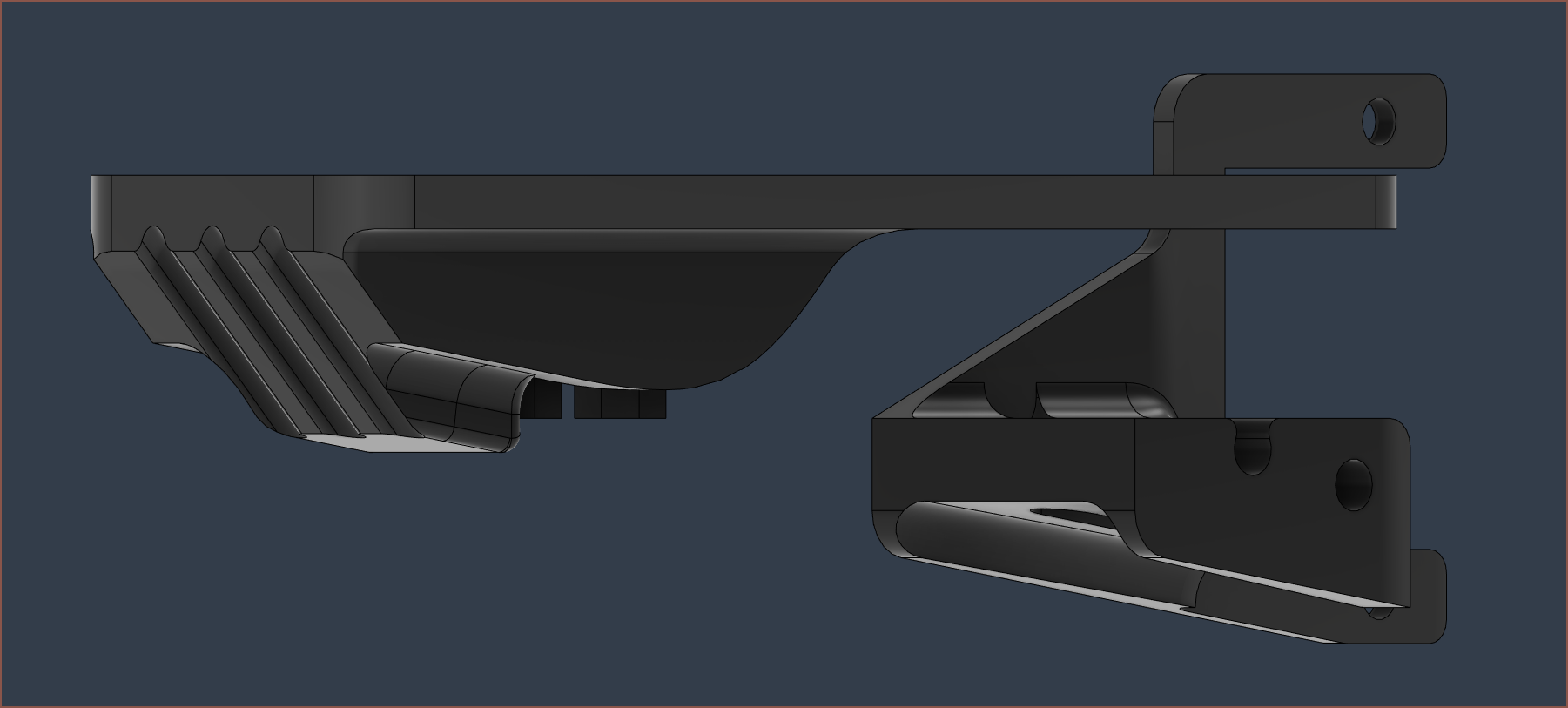
07/12/2023 at 18:44 • 0 commentsI knew I was going to get to a point where I wouldn't know how to go about modelling the rest of the enclosure / skeleton, but I modelled the section that I could.
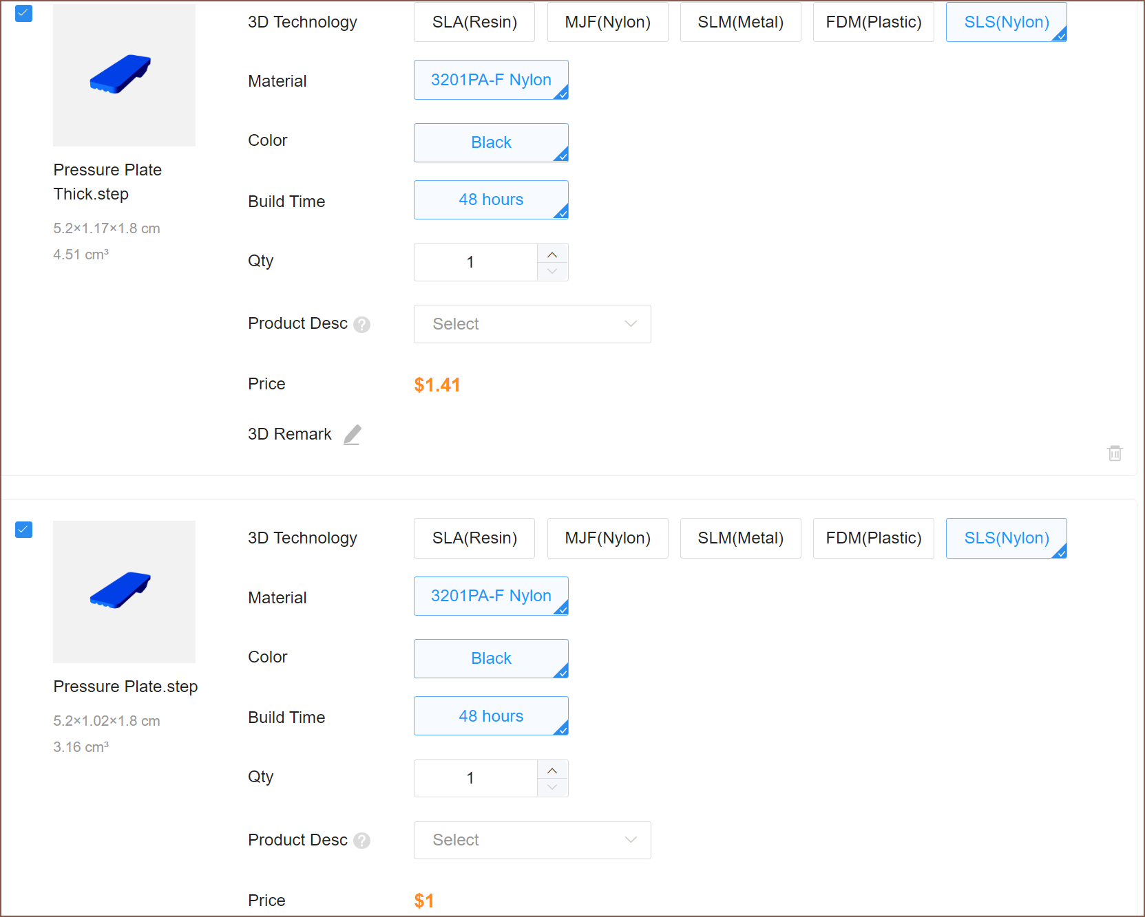
This all started by first looking on JLC for prices in MJF and SLS, mainly how big could I go until I was charged more than $1/part. It seems that adding a 1.5mm thickness to the pressure plate (for a Tetrinsic that's got nothing fancy happening like a solar cell or LCD) is where I go over $1, and by a good 40% increase. It's probably best to just keep with the normal pressure plate and then stick a 1.5mm peice ontop as then a vast array of colours and finishes are available for the visible part of the Tetrinsic.
And these are the other parts:
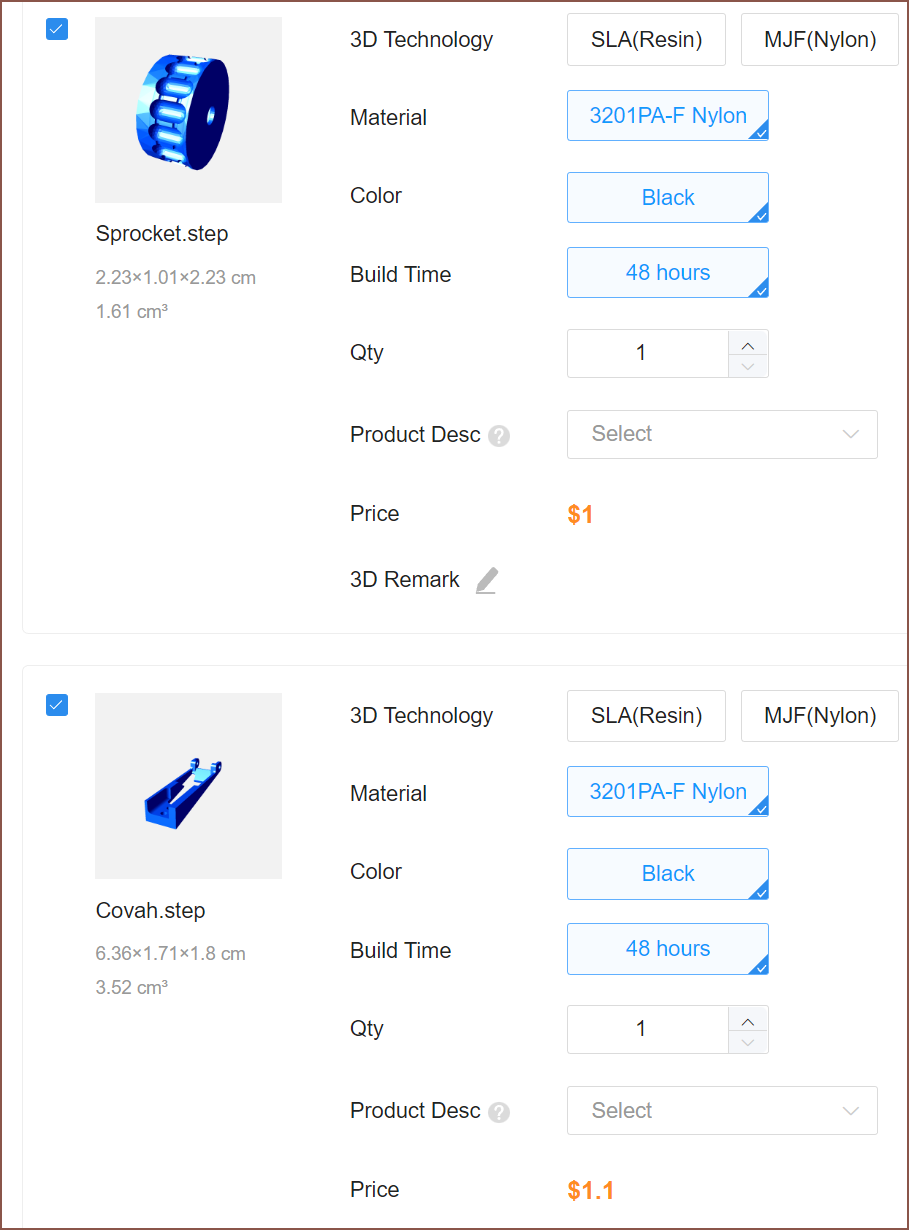
Covah.step is the skeleton (and is a temp name that is intentionally misspelled "cover"). The reason why I'm trying this is partially because I'm trying to think of a solution to actually holding them in place in the Proof Of Concept Tetent, which is almost the same as the fully featured one except that there's no battery and would only have 2 out of 4 Memory In Pixel LCDs.
The second is to allow easier integration into custom hardware designs.
Anyway, if all 3 parts were printed for 10 Tetrinsics, it'll cost £31.60 though I'd assume the shipping price would be bundled if also fabricating the PCBs though JLC too:
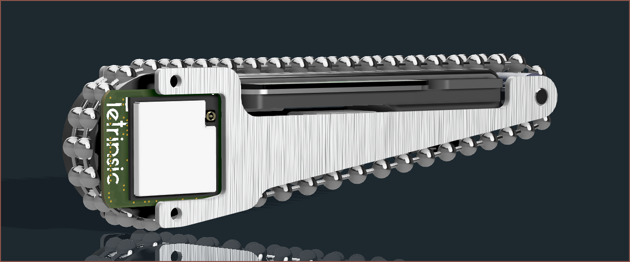
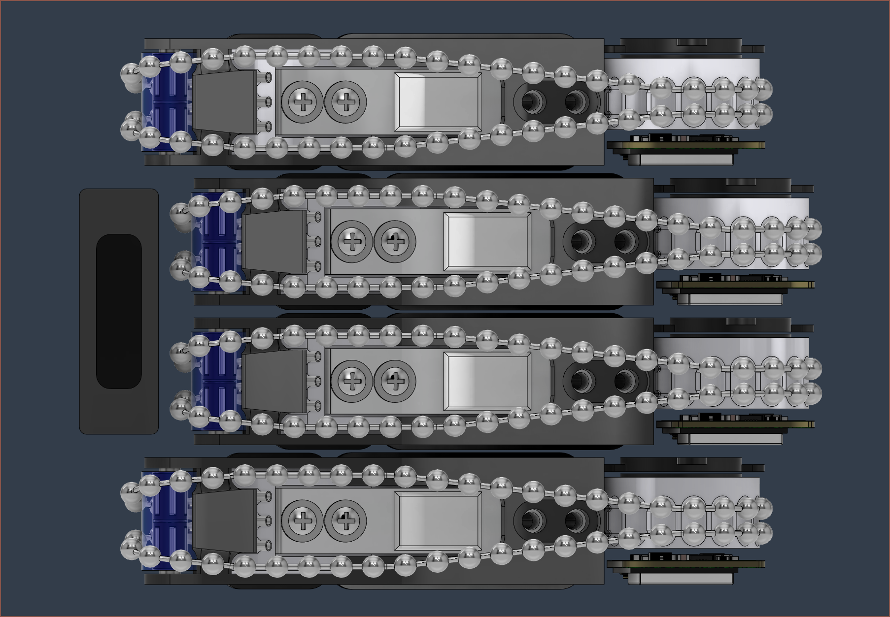
It'll look something kinda like the below, but this idea will only work if I somehow think of a way to mount the PCB.
Speaking of the PCB, I've been looking into panelizing 4 into a 50x50mm area as I hypothesise that I could get 20 boards (4 x 5pcs) cheaper than 10 boards (1 x 10pcs).
-
[P] 2.4mm and new 3.2mm chain
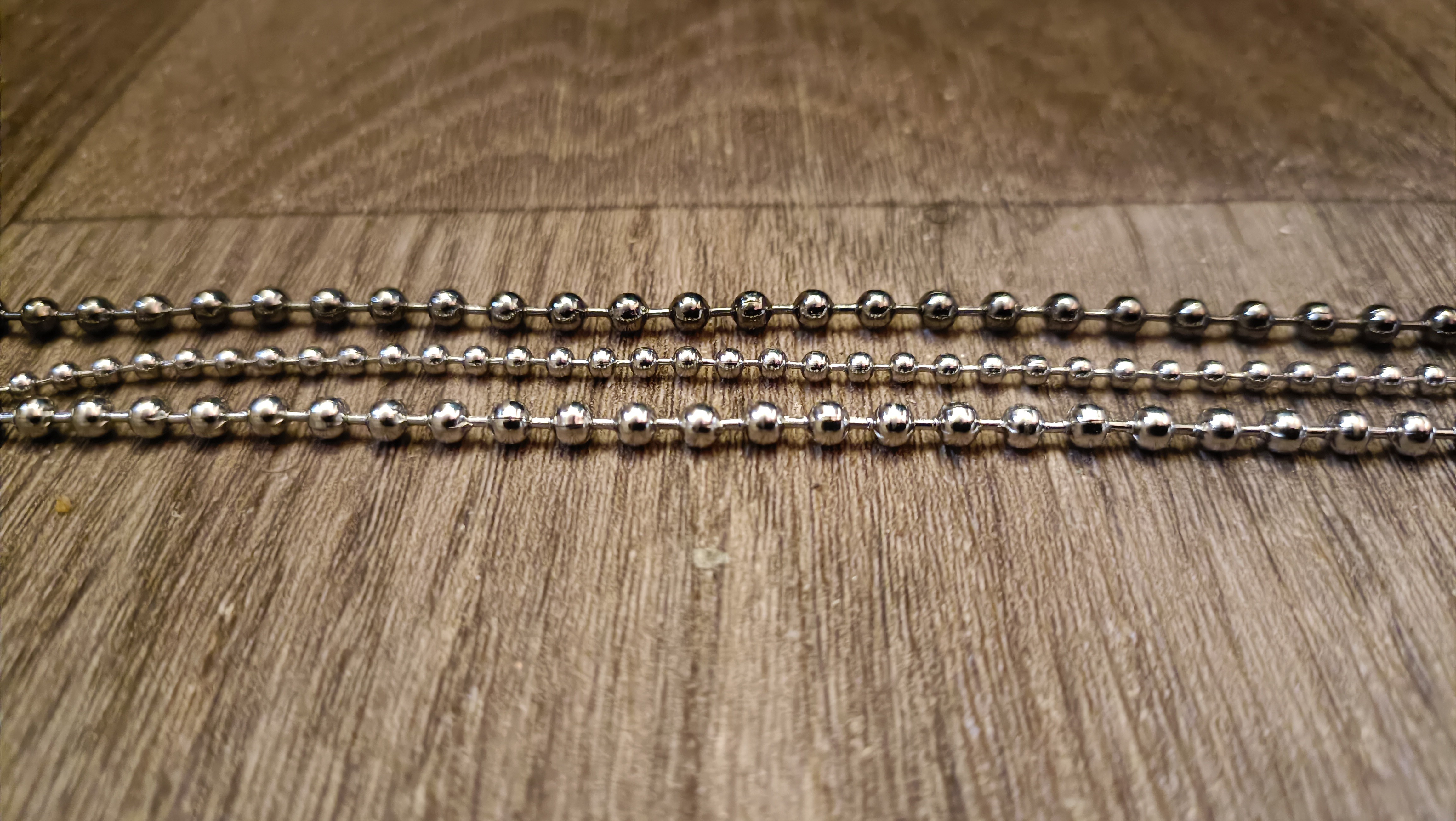
07/09/2023 at 17:42 • 0 commentsSo the 10m of 2.4mm chain arrived yesterday and it looked and flexed the same as the small sample of the stuff I've had since 2022.
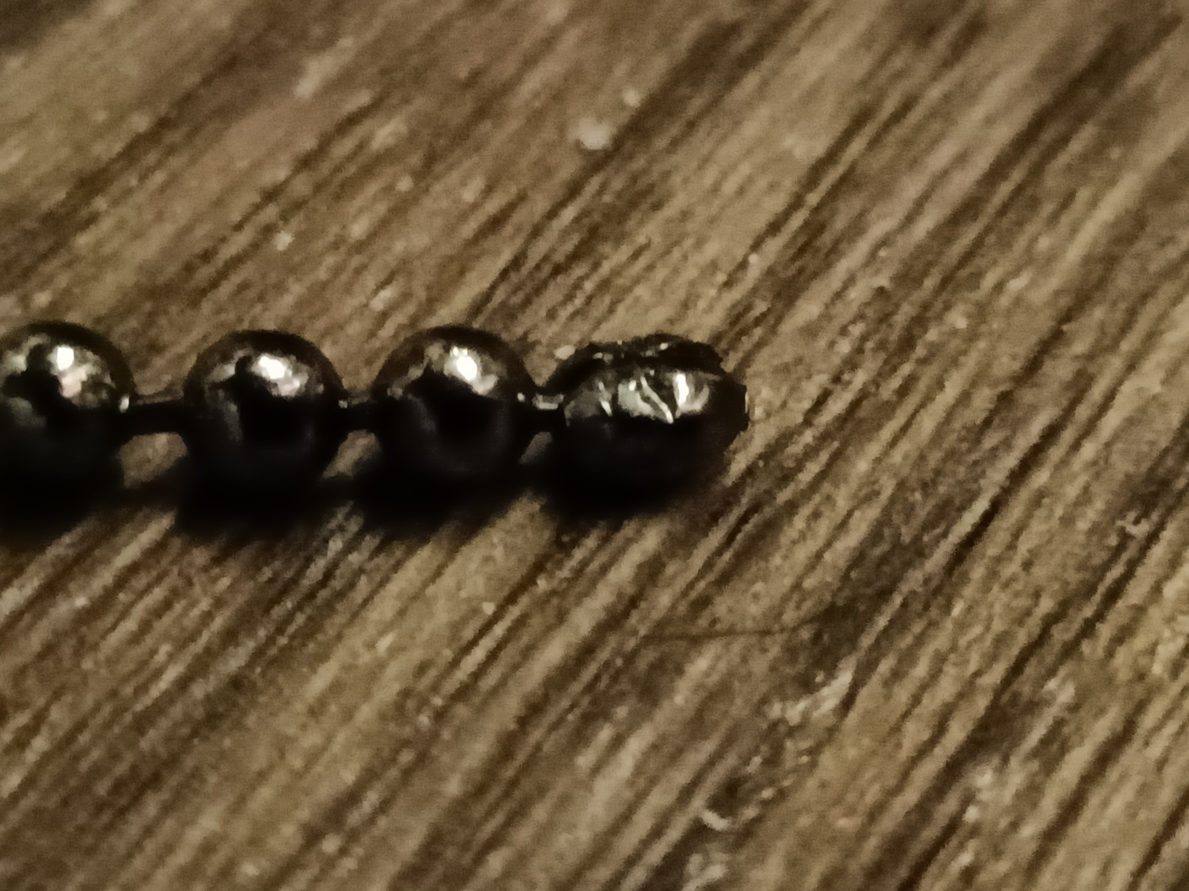
After seeing it, I went back to the dark 3.2mm chain and tried to see if I could scrape anything off the single crushed ball and I was actually able to get a tiny fragment of coating off, revealing the stainless steel below. It was then entirely possible that the reason for the large tensioned turning radius was due to the coating on the linkages. The 2.4mm chain slides on the linkages when on the bend, which doesn't happen with the dark 3.2mm. Thus, I found and bought another 3.2mm chain:
This literally-brand-new chain is the brightness I was expecting and it has a spacing of 4.55mm. It also goes around the OD 8.4mm pen-like scribe barrel much better than the used-like-new chain. This is good news since I was hoping that I could use 3.2mm chain for the #T^2 Tiles [gd0095] because, while it's twice the price of 2.4mm ball chain, it holds 20lb / 9kg more (source: www.ballchain.com), it should better resist slipping on the sprocket and it can be spliced into a closed loop.
It does seem that I should opt for a OD 8mm ID 5mm silicone tube instead of 7mm OD, wether I'm using the 2.4mm or 3.2mm. I still think the 3.2mm looks and feels better, so I'm going to revert in the CAD file.
Parameters of this new SourcingMap 3.2mm chain:
- 3.20 - 3.25mm balls, most commonly 3.23mm
- 0.77 - 0.80mm linkages, most commonly 0.79mm
- 4.55mm spacing
-
[P][T] Scribe Tool, 2.4mm Chain and Aluminium PCB Load Cell?
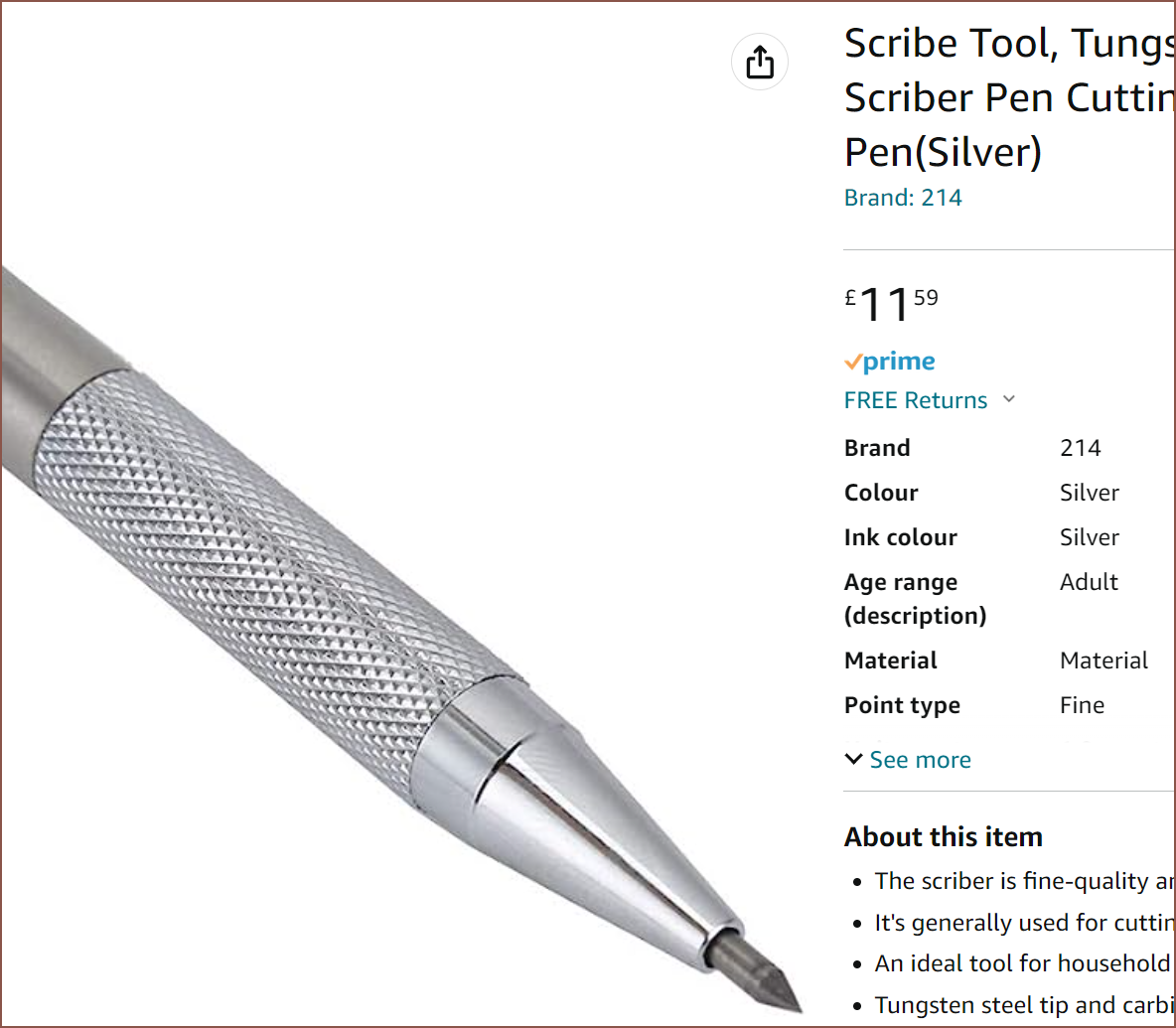
07/07/2023 at 23:23 • 0 commentsSo, this morning, I bought this scribe for £5.01:
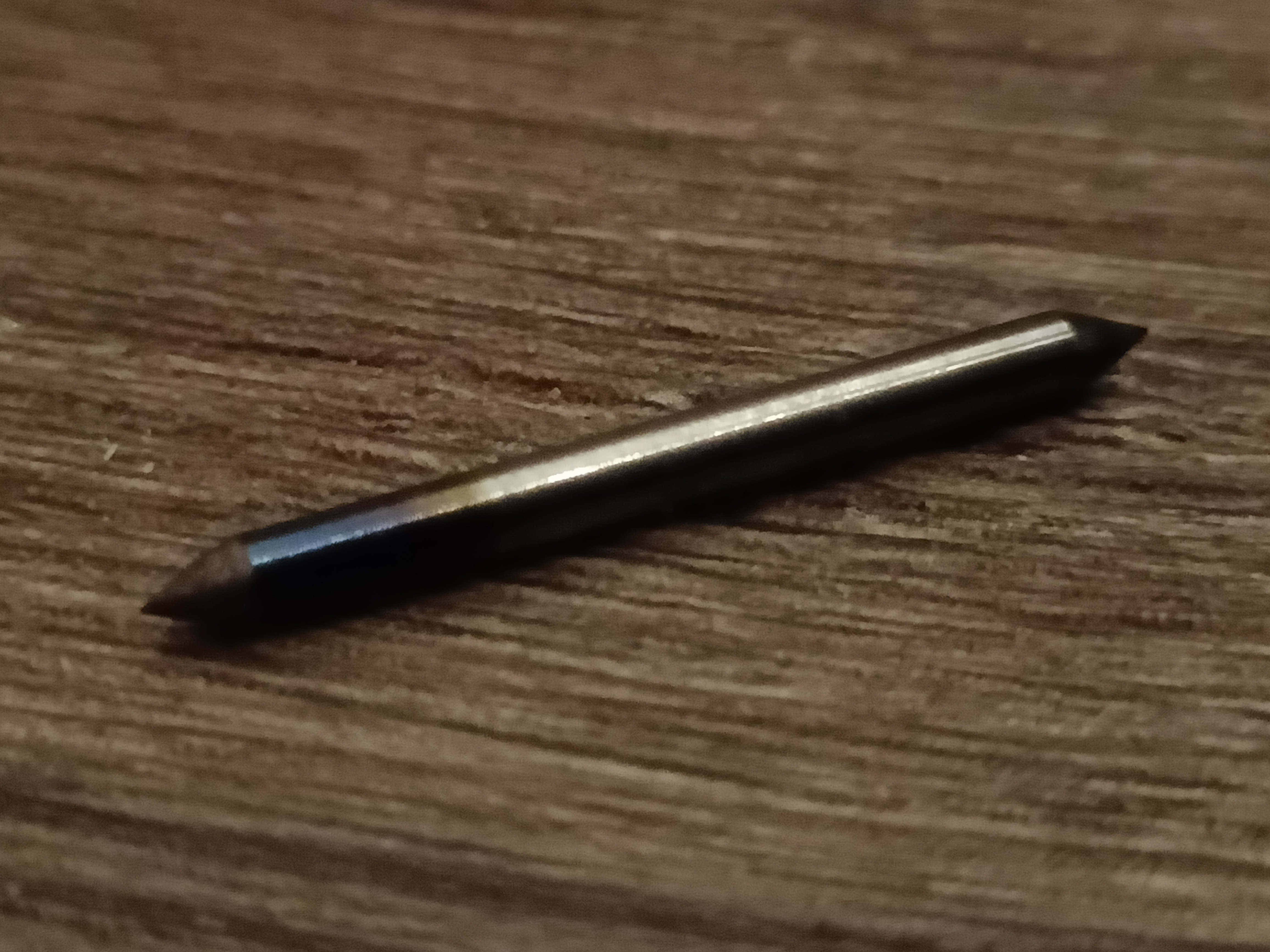
This is to get at it's scribe tool, which is 2mm in diameter and 24mm long:
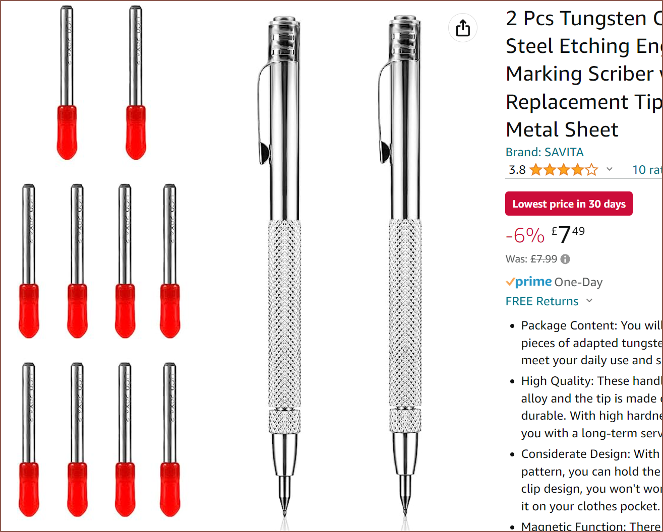
I was expecting that it would be flat on the other side, such as in a different product:
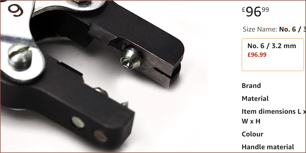
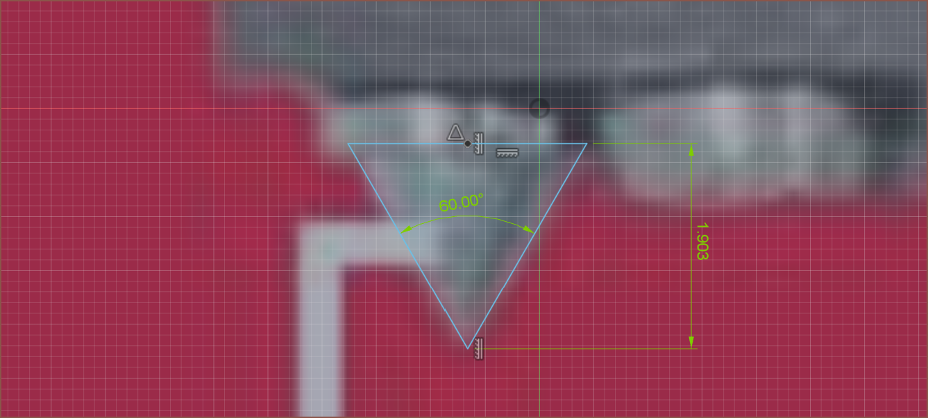
This means I'd probably need a design that uses a grub screw. I got this after measuring the angle of the £100 tool and then looking for anything with a diameter less than 4mm that has a similar point.
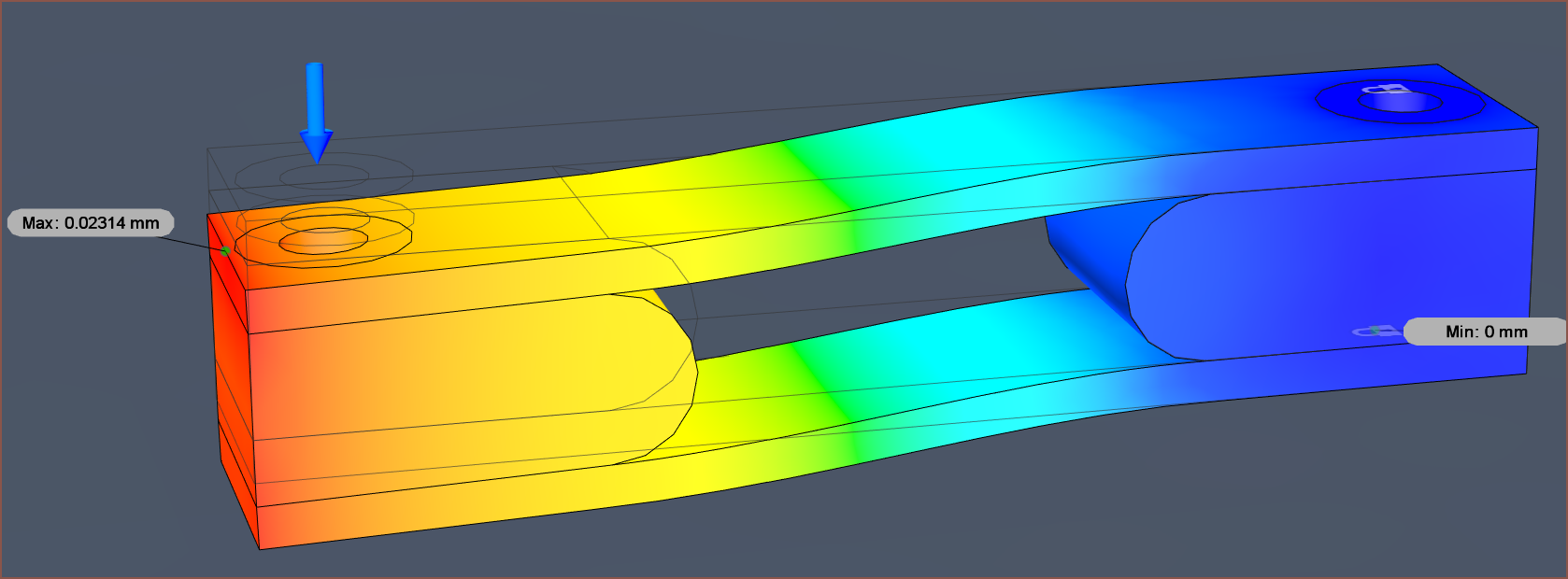
I then was reading through past logs, and one time I tried designing a PCB load cell. It seems, however, that I never tried simulating an aluminium PCB, which could cost under £5 from JLCPCB. The results with or without SMD resistors isn't that promising, but at least the deflection is less than 0.1mm:
The bigger issue is the turning radius of the sliding medium. I found the small section of 2.4mm chain and, unlike the 3.2mm stuff, it can actually go around 7.5mm diameter bends just fine.
Another consideration is that it actually turns out that my fingers easily use up the entire length of this new 52mm solution, though the utilisation would be better if the motor sprocket didn't force the Tetrinsics to be so close to the edge:
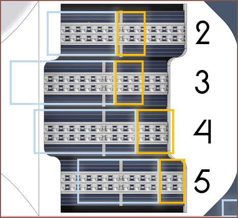
The orange section is the length of chain that would work for a pull-trigger style input, like what I'm doing on Finger5 for the shift key. Another way to put it, the boundary of the blue and orange boxes is where my fingers naturally rest. As long as all fingers can cover over half of the length (26mm), it should be fine. The earliest Tetrinsics designs only had 24 or 32mm of active area anyway. 52mm is about the spacing between 3 rows on a traditional keyboard.
-
[P] 3.2mm Ball Chain (and 100th log)
07/06/2023 at 22:31 • 0 commentsAlmost 1 year after I saw the beginning of the end for #SecSavr Sublime [gd0036], this project has overtaken it's 99 logs. There's only one other project -- a prism laser scanner -- that I know is in the triple digits. I'm not entirely sure how such a number of logs has accumulated and I'm only now looking to turn concept into reality, but I've got to take the few-and-far small wins on this journey whenever possible.
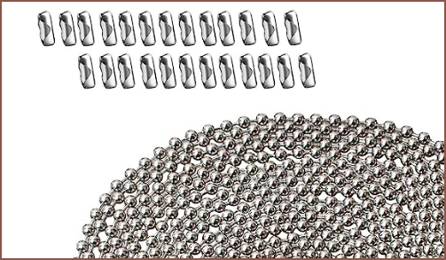
The 3.2mm "Used, Like New" ball chain just came in the mail from Amazon, and... it's certainly different from the image in 2 ways:
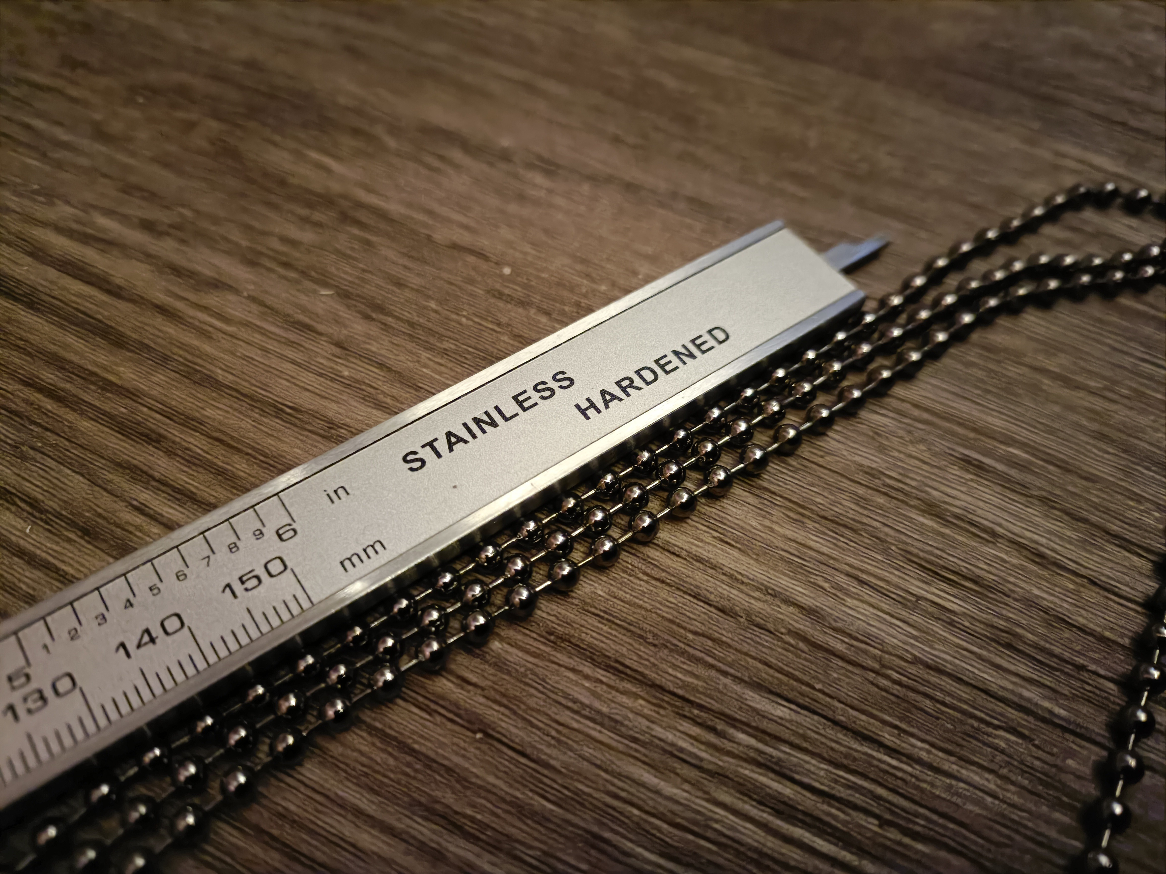
Firstly, there were no connectors in the bag I've got (or the packaging). That's fine since I wasn't planing on using them anyway. Secondly, as can be seen next to my calipers, it's visibly darker than anything I know to be stainless steel.
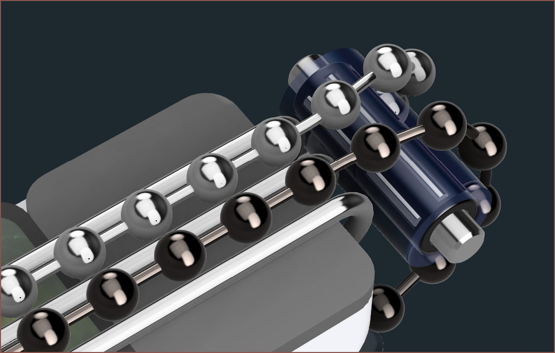
I've changed the texture of one of the ball chain loops to try and match what they look like in contrast to the default stainless steel texture. I think it looks a tad more premium this way, so I'll let it slide up until it starts rusting (implying that it was never stainless steel to begin with). Actually, it could just be more susceptible to lighting conditions than other metals. If I go under a brighter light, the chain still looks darker than other metals but it no longer has that slight brownish tint.
Other measurements are that the spacing between balls seems to be 4.9mm (measuring 14 balls to be 68.8mm), the linkages are 0.75mm and the balls are in the range of 3.18 - 3.24mm.
I'm going to need to model a sprocket to replace the small pulley. The reason is because, unlike in simplified physics calculations, friction is not negligible. It seems that, when taught, the ball bead binds on the linkage, resulting in a turning diameter of about 26mm.
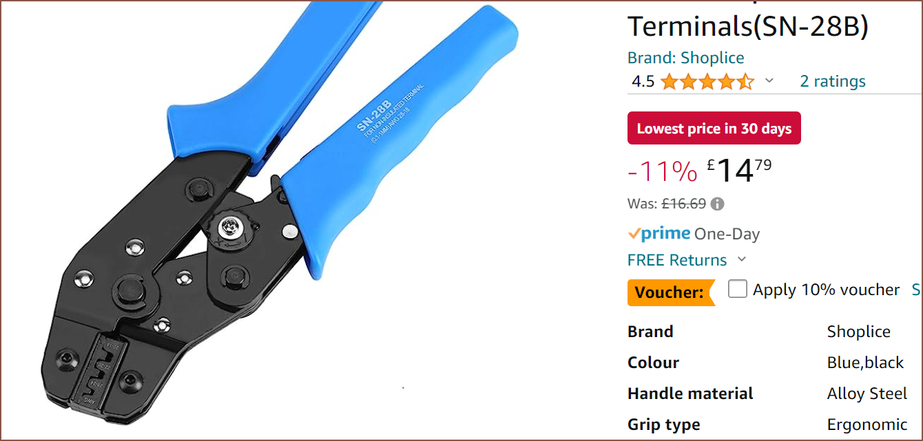
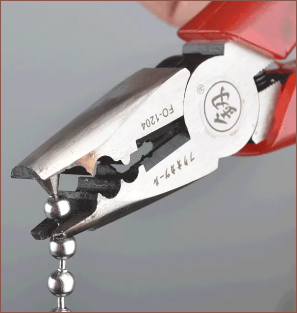
I'm also going to have to stop and think about the splicing situation. It certainly seems that I need the mechanical advantage of a crimp tool to actually do anything to these balls, but I'm sure not going to get the correct outcome from them:
I think the first strat I'm going to try is to replace the jaws of the SN-28B to be more similar to the splicer tools:
Obviously, this isn't a critical problem like the pulley is, since I could always fastpass my way to spliced chains by just buying the tool instead of inventing yet another thing here. It's not like I want this to be the difference between walking out of summer break empty handed or not.
-
[E1][R] LT6911C HDMI to MIPI in a QFN Package?
07/06/2023 at 11:05 • 0 comments[12:05]
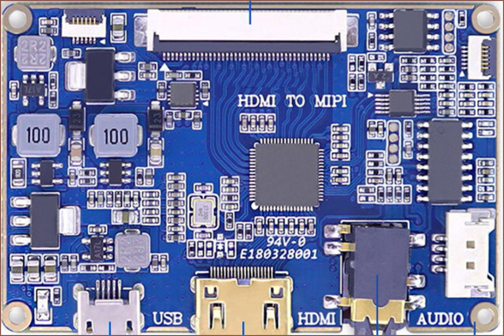
So, before I started creating a devboard that included the TC358870XBG, I wanted to see if I could find whatever QFN chip is used for the ET01-4K-V3.0 -- a named HDMI driver board on Alibaba:
This is because It's probably easier to route out than the TC, which is a BGA package. Searching HDMI to MIPI QFN lead me to the LT6911C and LT6911UXC,.The LT6911C supports HDMI 1.4 whereas the LT6911UXC supports HDMI 2.0. On AliExpress, it seems that the former is around £6 anf the latter £9, wheras the TC358870XBG is £4.
The freely downloadable brief was extremely brief, so I messaged as many AliExpress sellers of the LT6911C as I could find and I received some documentation that at least mentioned the pinout of the chip. Unfortunately, out of all 64 pins that the chip has, I couldn't see any mention of one that changed the I2C address. I did see that it's got an I2C for "EDID" and "Program Register", however.
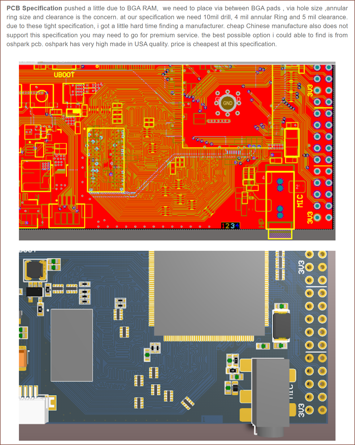
Looking at the above PCB, it's possible that this chip doesn't need an external microcontroller to initialise it, but since I don't have a fully featured tech document anyway, I'll move forward with the TC358870XBG, hoping that I don't need vias like what was needed for a DDR3 chip on a board I found on my research travels:
This was written in 2015. A 10mil drill = 0.254mm, which JLCPCB does these days (at an additional cost), but I think they'd also need 8mil (0.2mm) clearance. At least I found out that a 32GB chip of LPDDR5 is £23/each as a result of this research:
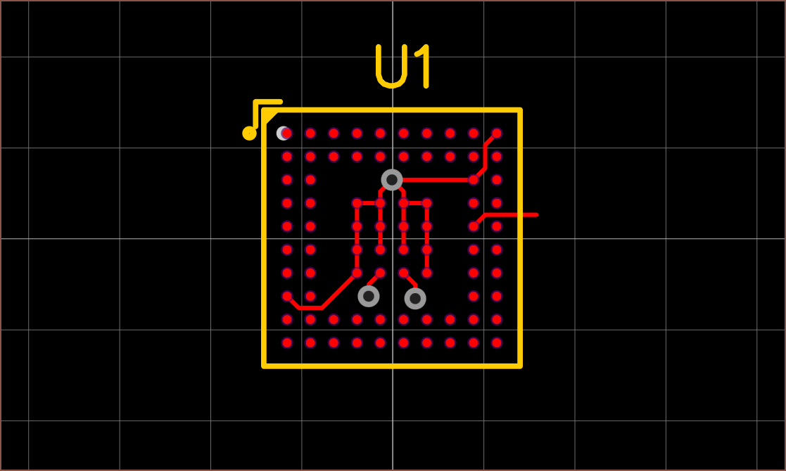
Now I'm wondering why laptops with soldered-on memory have such large price differences between RAM configurations, as well as why 32GB options are somewhat rare in the market. [17:40] JLC has the TC358870XBG and, as such, the footprint is available on EasyEDA. Very quickly looking over the pinout, it seems that the traces for the interior would look something like this:
These are 0.12mm traces with 0.12mm spacing set in the DRC. JLC claims that, for 4+ layer boards, their capabilities are down to 0.09mm track/space. They also say their minimum BGA pad size is 0.25mm, and they're 0.24mm in this EasyEDA footprint. The bottom 2 pads in the middle group of balls are for TEST and IR, and I doubt I'd be using it so it should "be fixed low", according to the documentation. I'm assuming they're saying to just connect it to ground. The TEST pin also has the note to always fix low externally too, so it's probably safe to assume that entire interior section can just be one GND copper pour.
In any case, all this talk about HDMI to MIPI bridges are irrelevant if the Tetrinsic proof-of-concept ergonomically fails.
Tetrinsic [gd0041]
A motorised fader that is continuous, pressure sensitive, haptic and water resistant.
 kelvinA

 It's also interesting to know that I'm now at save v359. Only the
  Tetrinsic Taic looks really cool and every past version of myself in the last 15 or so years (whenever the




 I knew I was going to get to a point where I wouldn't know how to go about modelling the rest of the enclosure / skeleton, but I modelled the section that I could.

 So the 10m of 2.4mm chain arrived yesterday and it looked and flexed the same as the small sample of the stuff I've had since 2022.

 The 3.2mm "Used, Like New" ball chain just came in the mail from Amazon, and... it's certainly different from the image in 2 ways:
 Firstly, there were no connectors in the bag I've got (or the packaging). That's fine since I wasn't planing on using them anyway. Secondly, as can be seen next to my calipers, it's visibly darker than anything I know to be stainless steel.
 I've changed the texture of one of the ball chain loops to try and match what they look like in contrast to the default stainless steel texture. I think it looks a tad more premium this way, so I'll let it slide up until it starts rusting (implying that it was never stainless steel to begin with). Actually, it could just be more susceptible to lighting conditions than other metals. If I go under a brighter light, the chain still looks darker than other metals but it no longer has that slight brownish tint.