-
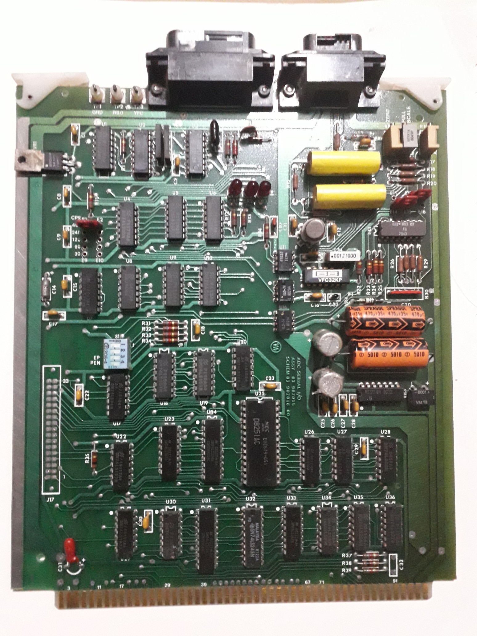
ADC Serial I/O Board
12/06/2022 at 18:11 • 0 commentsThis board turned out to be far more complex than expected. There are three connectors on the board - a large 24 pin connector wired to the 8251 PCI, a 14 pin connector wired partly into the digital side, and partly into the analogue side, and an unpopulated 34 pin header.
Based on the probing so far, I suspect the 14 pin connector is the link to the chromatograph machines, and it has some bit-banged protocol driven directly by the CPU when needed. I haven't looked into the analogue circuit yet, but I assume it's an ADC and associated reference voltages. A couple of optoisolators link from the digital side.
The 34 pin header I am guessing is for attaching a precision ADC. It consists of a read-only 14-bit parallel interface, read as an upper 6 bit number with a seventh bit fetched from elsewhere, and a lower 8-bit number, mapped into different addresses. The address used to write to the analogue port is the same as the address used to read from one of the header addresses, which, combined with the 14-bit data length, is what makes me think its ADC related. None of the four boards I have have this populated, so it was clearly an optional extra.
The serial port is a centronics-style socket so I will need to make an adaptor or wire another socket directly to the board to make it talk to anything else.
The schematic is unfinished and needs rearranging because it turns out chips are scattered all over the board with no regard for which other chips they are connected to. The logic surrounding what are supposed to be the interrupt and acknowledge signals makes no sense in this context, so I think these pins have been repurposed. In particular, Int7 and IntAck7 are wired into the chip selects, and I assume are hardwired on the backplane to give each of the four serial slots a unique address. Having a backplane to look at would make this much easier.
![]()
-
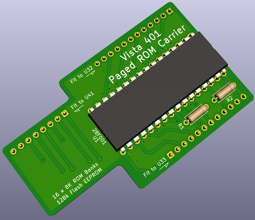
ROM Board Updates
11/30/2022 at 20:07 • 0 commentsFurther examination has placed EPROM U19 at memory address &6800-&6FFF. EPROM U9 appears to have its address decided by the contents of the two 7641 ROMs. Extracting the ROM contents will, presumably, reveal more - perhaps the EPROM moves around or is mirrored into several blocks of memory.
All 19 of the MK36000 ROMs have extensive corrosion on the pins, and only three came out without losing at least one pin. The EPROMs and 7641s are all unaffected. As modern EEPROMS aren't pin compatible with the MK36000s, I will likely replace the 16 paged ROMs with a single 128K EEPROM on a carrier board, and have another EEPROM replacing the fixed ROMs. For initial testing, I will likely just use jumper wires to connect U18's socket to a breadboard or stripboard adaptor, and leave the paged ROMs and other fixed ROMs empty. The OS ROM will probably be replaced by a 28C256 with some diodes and flying leads to the two secondary chip selects - I've built something similar for my BBC Master's paged ROMs.I have knocked up a possible design for the paged ROM carrier board, which sits across U32 and U33, as well as picking up the bank addresses from U41 (which will need to be removed and replaced with a socket).
![]()
-
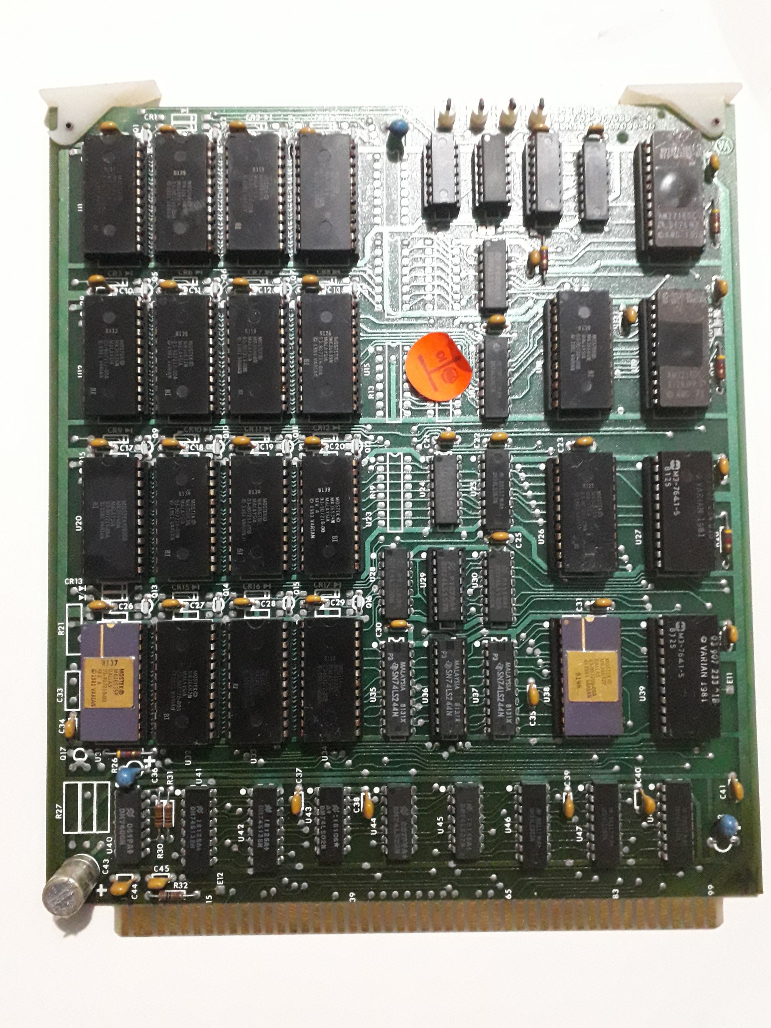
Rom Board & Memory Map
11/28/2022 at 17:19 • 0 commentsThe ROM PCB seems to be split into three primary sections:
The left hand side consists of 16 8KB mask programmed ROMs, addressed via two 3-to-8 decoders. These are the system's paged ROMS.
The mid-section consists of 3 8KB mask programmed ROMs, permanently mapped into the address space. These are presumably the core OS.
The right hand side consists of 2 512B mask programmed ROMs serving as some kind of additional address decoding logic, and 2 2KB EPROMs. I have yet to work out where these two EPROMs sit in the address space visible to the CPU.
The memory map, thus far, appears to be as follows:
Start End Contents 0000 1FFF Fixed ROM U18 2000 3FFF Fixed ROM U26 4000 5FFF Fixed ROM U38 6000 7FFF undefined 8000 9FFF Paged ROMs A000 BFFF undefined C000 FFFF CPU local RAM I haven't looked at the RAM card yet, but I assume there will be a 3-to-8 decoder mapping that 64KB into 8KB pages in one of the two undefined spaces.
The paging latch on the ROM card sits at IO address 0110xxxxb. Rather than latching the data bus, it latches the lower four bits of the address.
![]()
-
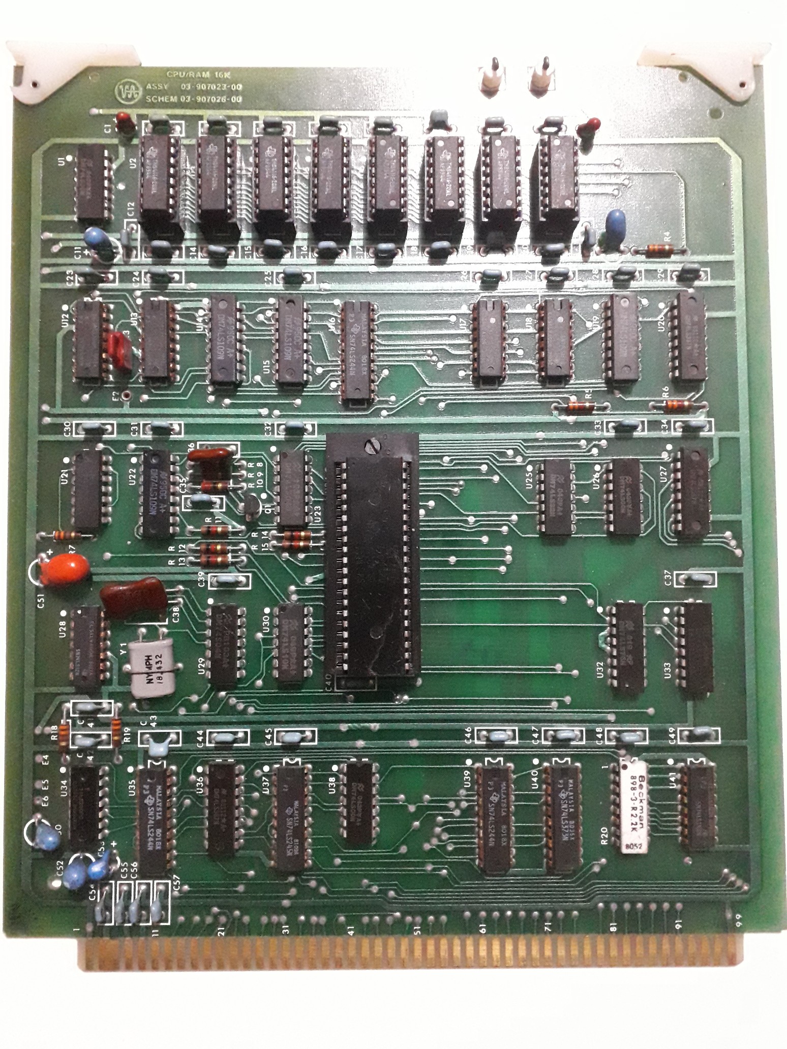
CPU Board Update
11/27/2022 at 16:02 • 0 commentsUpdated the CPU board schematic - added all the non-IC parts (resistors, capacitors, two test points, one jumper and one transistor), fixed up some errors on the previous version. Worked out how the data bus enable logic worked, and it does seem to switch off when reading from internal RAM (but not when writing, but presumably address decoding on the RAM card means this is harmless). Still not entirely sure what some signals do, but I think there's enough done now to get it talking to the ROMs, so I shall make a start on that card next.
-
CPU Board Progress
11/26/2022 at 10:54 • 0 commentsThe CPU board is now almost fully probed out. The schematic is not the tidiest, but all the chips now exist, though a few pins still need checking out. A lot of the signals I can work out the function of from their connections to pins or other identifiable signals, but there are a few I'm still unsure about. There may also be some mistakes, I'll have to recheck everything once it's complete.
If I'm reading the /RAS circuit correctly, the onboard 16K of RAM sits in the uppermost 16K of memory from &C000 - &FFFF. Unless I'm missing something, I can't see any bank select logic on the board, so the RAM card must handle that itself. I also don't see anything to stop the address/data lines being active on the bus during access to local RAM, so I assume the RAM card must handle mapping itself into a suitable place in the memory map so it doesn't respond. I'd assume U37 needs to turn off though, so floating inputs on the BD[0..7] lines aren't making it try and drive D[0..7]. Maybe the /DBUSEn logic handles that.
![]()
Varian Vista-based Z80 Microcomputer
Turning a pile of old circuit boards into a working computer.