Close
0%
0%

CRAPi2040

Chris' Really Awful Pi: so bad, it's good

Similar projects worth following
The CRAPi2040 board is a RP2040 based development board that's so bad, it's good...maybe.

Pushing the limits of clever PCB design to make the last dev board I'll ever need.

Features? We got 'em. This bad boy has features creeping into every crack and crevice for no other reason than pure masochism and maximum usefulness for any project situation that I could think of.

In the order that I remember them:

- Exactly 1 square inch (that's a feature right?)
- USB-C, but skinny.
- ALL the GPIO of the RP2040 broken out plus some bonus pins
- breadboard-able and PCB-able
- LiPo Charger
- 4 LEDs (RGB + B)
- SMD Protyping Grid
- Truly "flippable" design
- Configurable power pins
- A user button! that can be broken out!
- QR-Code on the back for quick reference
- A nice picture of a happy fish (guess the type)

This is my entry into the Gearing Up phase of the Hackaday Prize - the dev board for every project.

I'll be honest: sometimes I do a project just for the end result. I know, I know, it's about the journey and the process and the friends you make along the way. I totally get it! But man, sometimes I just realllllyyy want the thing. And it seems like most of the time, the thing is powered by a microcontroller. But I have a simple mind. Much too simple to screw around with wacky custom software and toolchains and to pledge allegiance to some silicon overlord. That's what led me to this project, the CRAPi board. 


My two brain cells worked up a storm on this one. I needed the board to be cheap and flexible. I wanted this board to be like ketchup: put that sh*t on everything. That way I could stop thinking about making stuff and actually make stuff. What better sliver of silicon to use for this noble goal than the RP2040? For the price and the PIO capabilities, it fit the bill. That's just the beginning though.

A wise man once told me "Pads are free, dude." And I took those words to heart. How could I squeeze every last bit of usefulness out of the thing that is literally holding the circuit together? Well for one thing, it meant that I didn't need to mess around with a USB-C connector. Upon seeing my substrate only USB-C pads the wise man promptly replied "Well that's a CRAPPY idea." And oh man was he right, that is a crappy idea. But why not try it anyway?


At it's core the CRAPi board is really about being an all purpose dev board without being too flashy about it. What was supposed to be an awful little weekend project to see if you could really make a USB-C connector just out 0.6mm PCB  turned into months of purely indulgent feature creep, masochism, and thoughtful design PCB design that borders on unhealthy.

  • Battery Mystery Solved (and more wire bonding by hand)

    Chris01/29/2024 at 01:21 0 comments

    A short log with lots of eye candy, but perhaps one of the most triumphant logs yet! In short, I have had trouble with my charging IC for the past few months. First, it wouldn't charge all the way, and the light would remain forever red. Second, it would stay green (reporting fully charged) even with no battery connected. This is undesired behavior which was not present on Rev. 2 of the boards, which only suffered from the former issue.

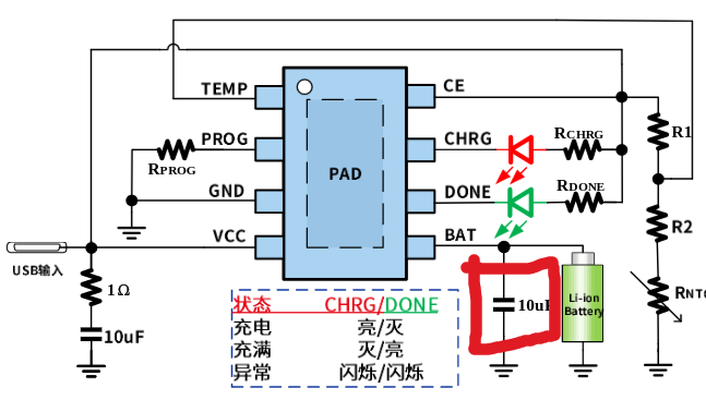
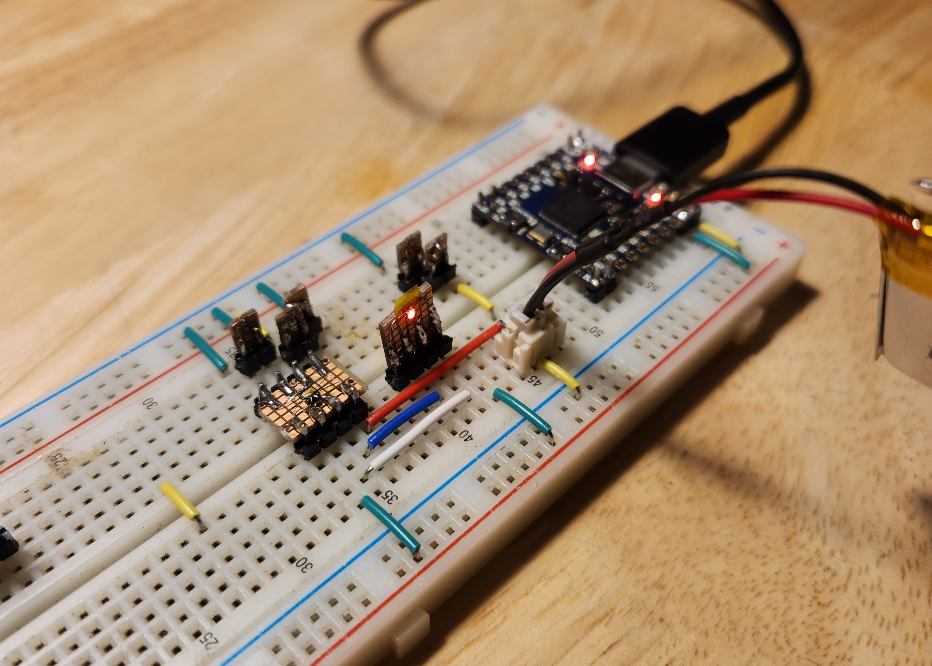
    I realized that if I want the DONE and CHRG  light to both remain off while there is no battery connected, I need to remove the suggested capacitor at battery input.

    I guess it makes sense that the chip behaves this way. From what I can tell, the IC is essentially charging the capacitor to a little over 4V and then reporting DONE. Based on some probably erroneous calculations, the capacitor is being charged at about 3 uA and has a DC impedance of about 1.32 MOhms.

    This chip does have a low current "trickle charge" meant to revive dead cells. It's possible that 3 uA is enough for the chip to operate in that regime and enable it's constant current supply into the capacitor.


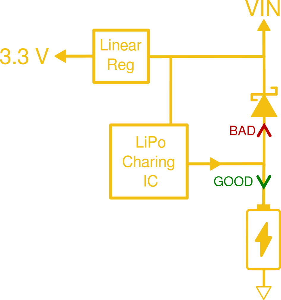
    Either way, I get my desired behavior when I remove the input capacitor. This seems like a bad idea, because it is. Without this capacitor, the CHRG and DONE light flip out when I press my finger to the contacts while the battery is disconnected and who knows what sort of instabilities that could lead to. I wonder if I can just use a TVS diode to kill any transients. I found a 0201 TVS diode with a leakage current of just 0.2 uA. Maybe that will be low enough as to not trigger the charging IC while still providing some transient protection.

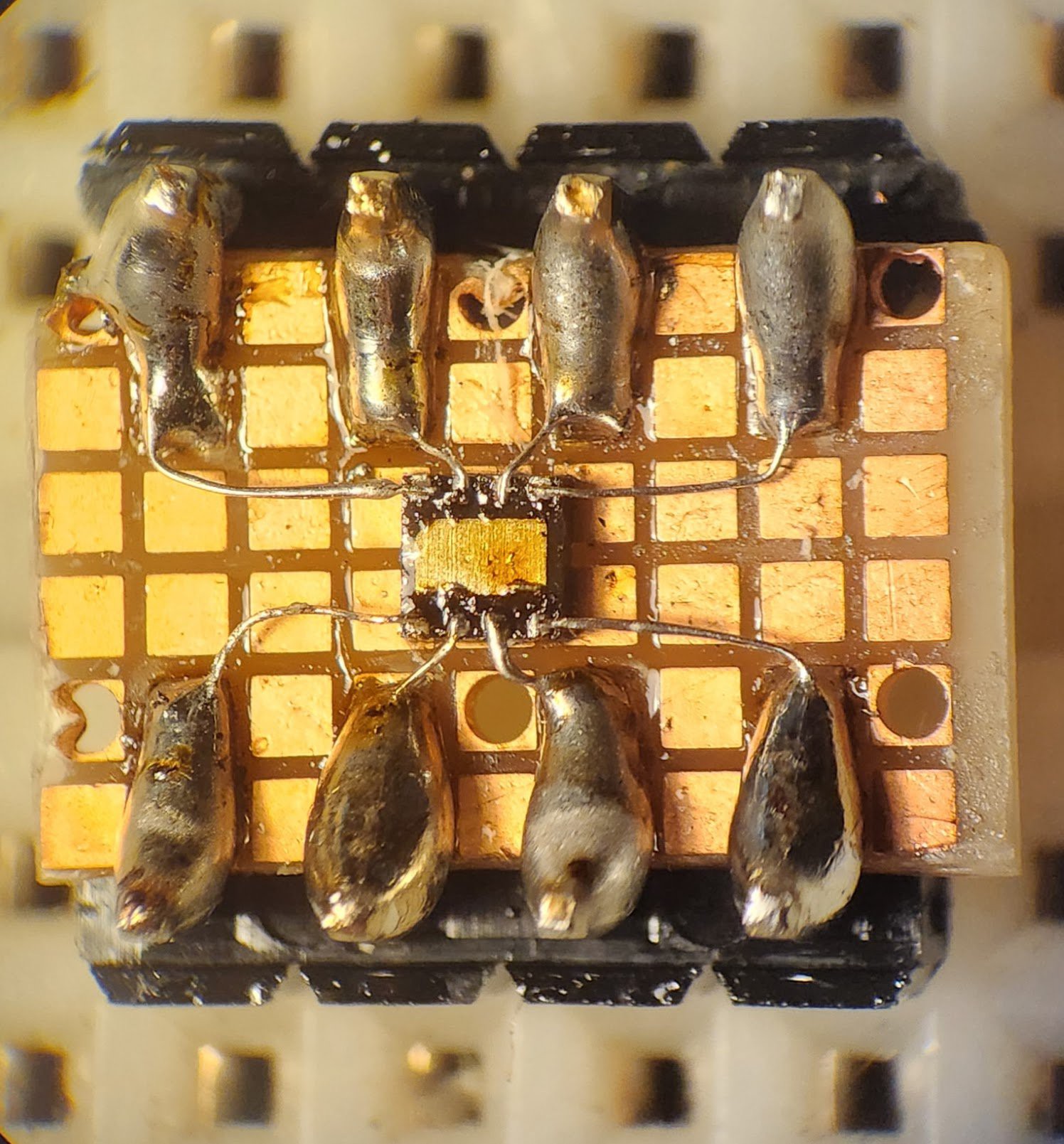
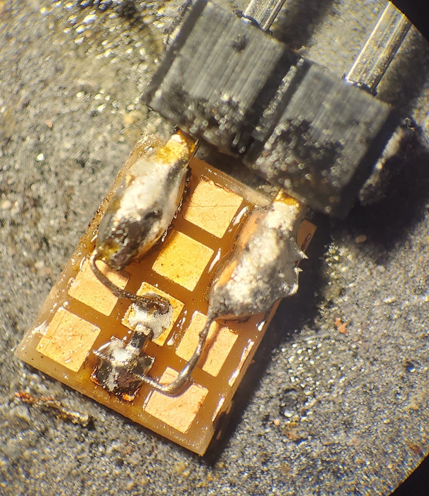
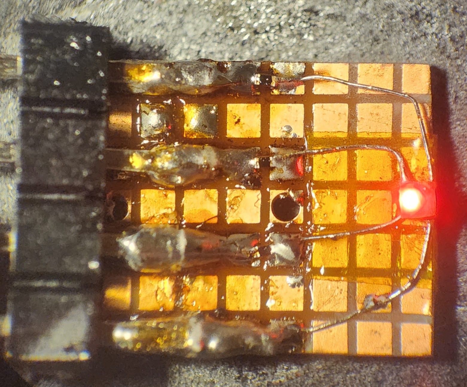
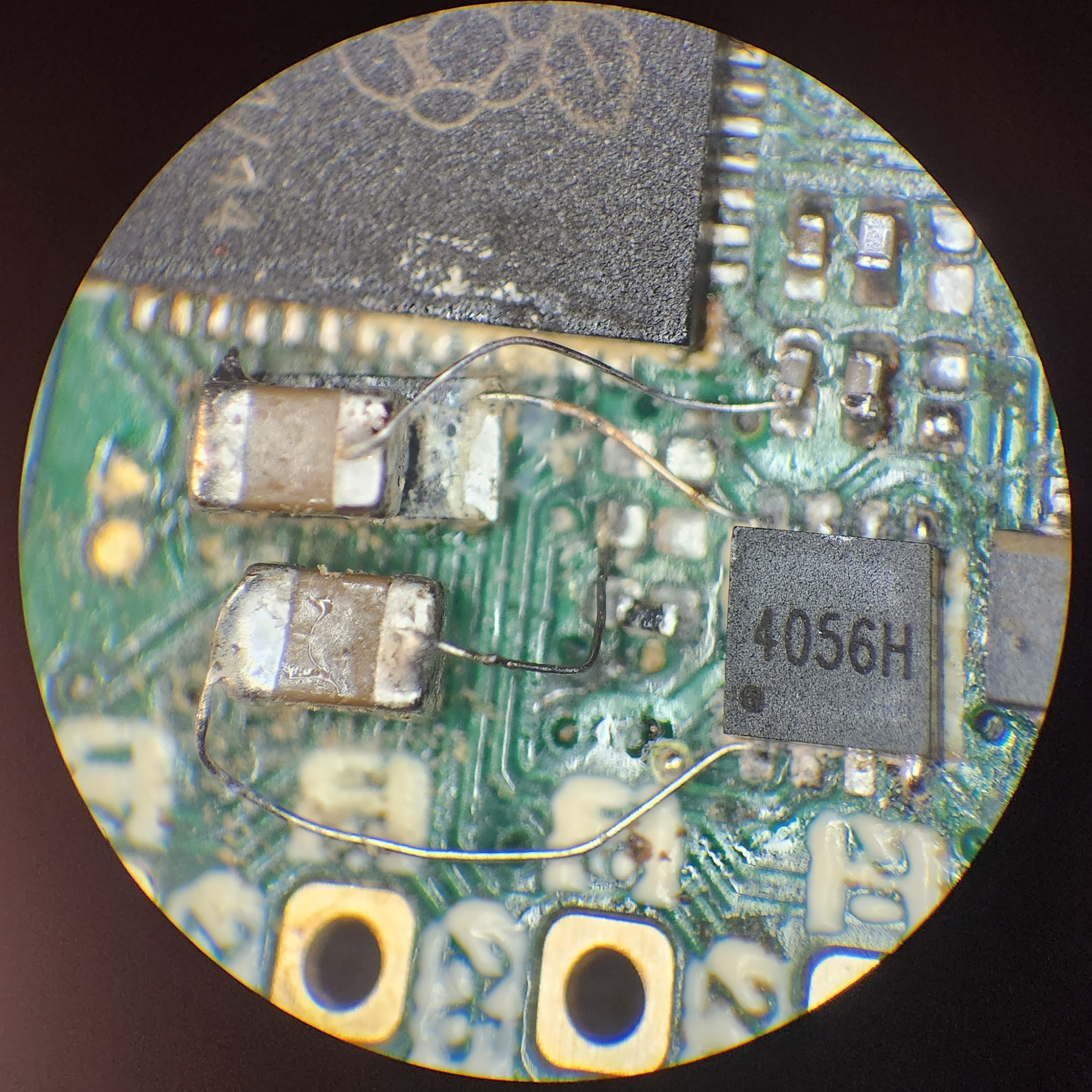
    How did I figure all of this stuff out? I breadboarded! How do you breadboard components that could fit through the eye of a needle? Just check out the pictures below...

  • CRAPi Rev. 3 is Complete (thank you PCBWay)

    Chris11/28/2023 at 04:47 2 comments

    That's right, Rev. 3 is basically complete and the board is almost ready for public consumption! There are a few different changes that I will get to but first:


    A huge thank you to PCBWay for sponsoring this run of pcbs!

    While PCBWay sponsored this revision of the CRAPi board, all of the following opinions are my own.

    A rep from PCBWay reached out to me after my last post and thanks to his incredible generosity I was able to check out their services. I had never used PCBWay before so I didn't  know what to expect, but right off the bat I noticed that the customer service was impeccable. They have a great intake system that let's you correspond with the representative responsible for your boards directly from within the website (as opposed to an email chain). My absolute favorite part of their website was the real time tracking of the PCB production stages. It's really cool to know exactly what stage of the production process your board is in and know when progress is being made.


    Really the only negative aspect (which isn't really negative at all) of the proofing process was the final cost/capability assessment. PCBWay takes a very professional approach in their proofing process and if you mis-specify your required manufacturing capabilities (trace width, drill diameter, etc.) they will ensure that those specifications are corrected and that your PCBs match your gerbers as closely as possible. This is in contrast to my experience with JLCPCB, who simply approved my design and sent it off for a best effort approach on their production line, resulting in different via diameters and trace widths than what I specified in my design.


    The proofing process resulted in a significant increase in the cost of the boards which was a bit shocking. Given that these boards were sponsored I choose to proceed with their recommended process specifications but in the future I would most likely work more closely with my representative to strike a balance between cost and specifications. It's clear that there is just a higher level of professionalism with PCBWay!


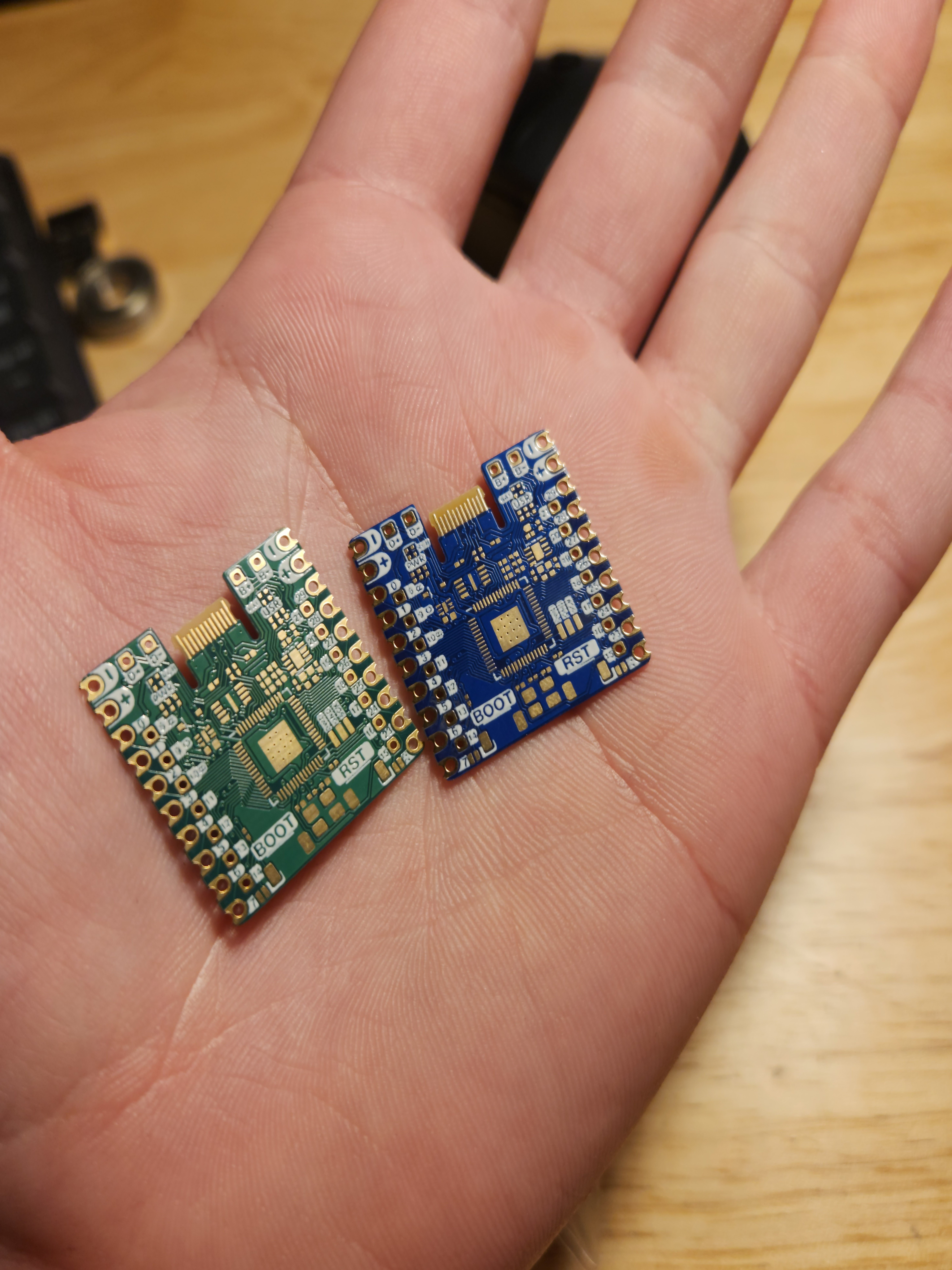
    Once that boards were done they arrived via DHL in just a few days. Incredible! I think they turned out very nicely.

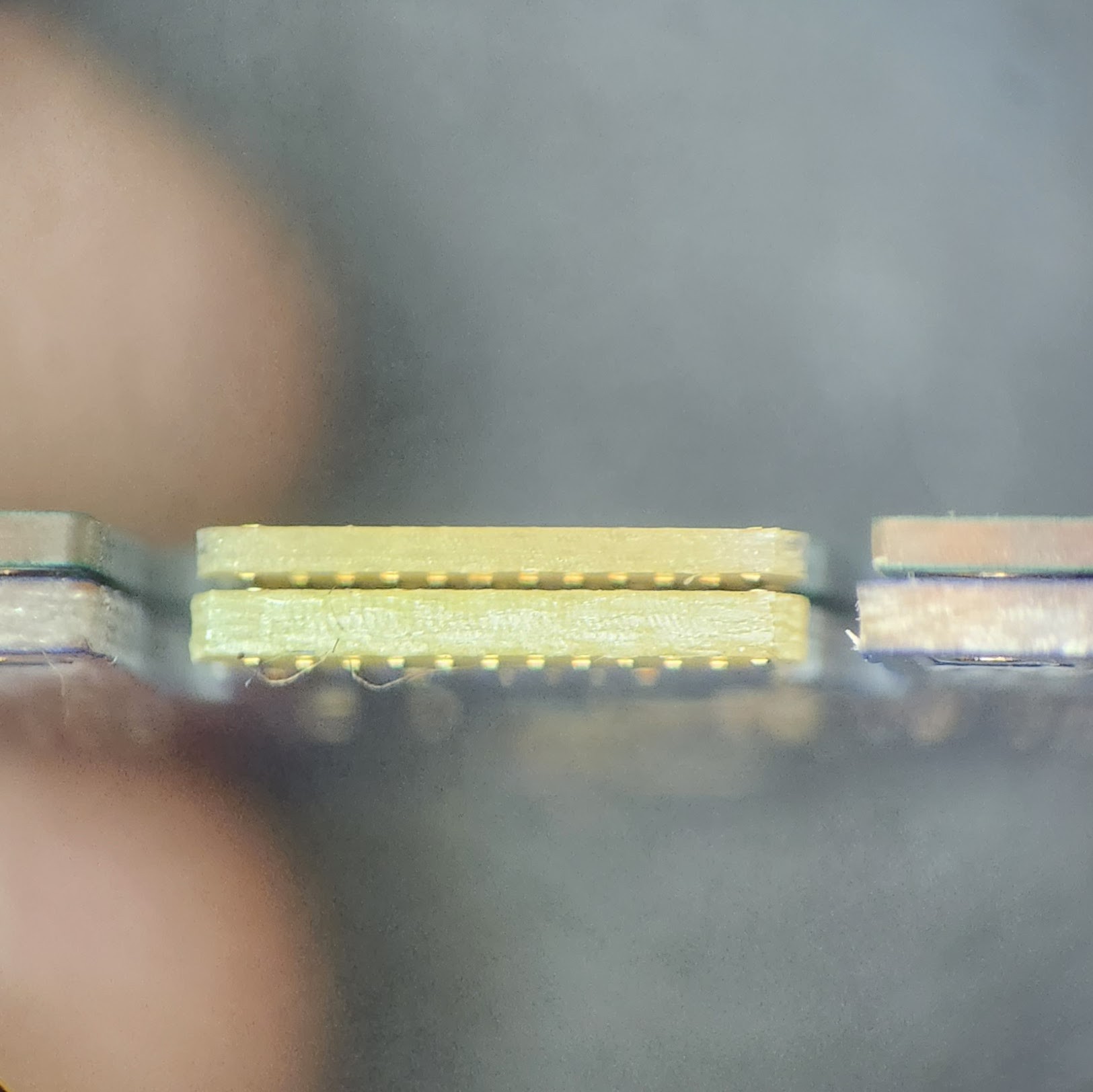
    This time around I was curious about how the thickness of the PCB would effect the retention force of the USB connector. The green boards are the 0.6 mm that I have used for the previous revisions and the blue board is 0.8 mm. The USB-C specification is 0.7 mm. The blue boards were almost impossible to disconnect accidentally. The force required to unplug it was almost too high. It also appears that the contacts on the blue board slowly get mushed down after repeated connections. I need to do some more repetitive testing before I decide on a final thickness and weight the costs and benefits of the thicker board.

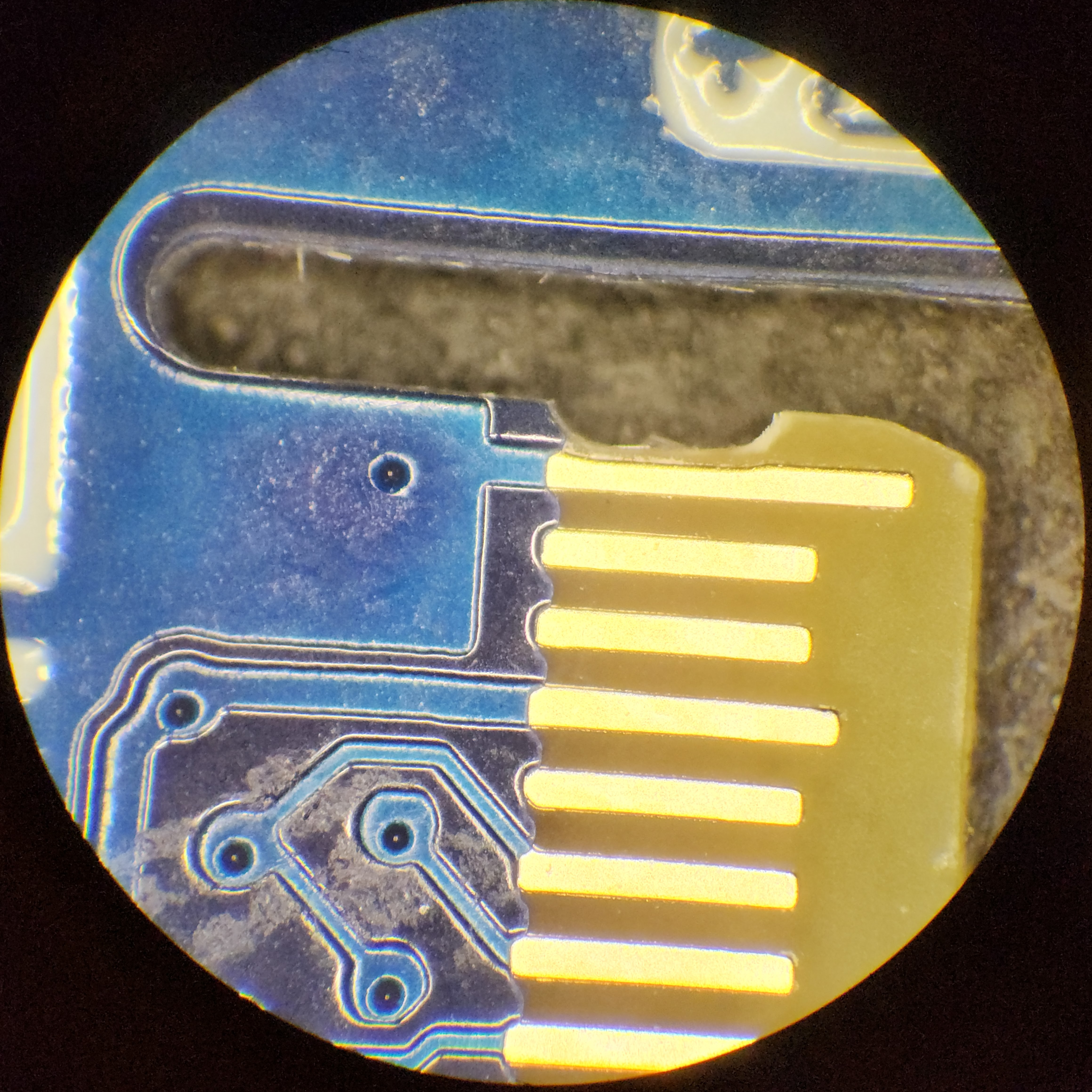
    PCBWay also did a superb job routing the small detents into the side of the USB-C connector. Previous revisions that used the JLC boards were far less crisp and the increase in quality is evident in the improved retention force of even the 0.6 mm thickness.

    Really the only criticism of their build quality was a slight mismatch on the registration of the vias. The vias uniformly off-center from their desired locations across the entire PCB. It's quite possible there could have been an issue with my gerbers, or that I am simply pushing the limits of their production capability. Nevertheless, they were all consistently covered with soldermask and this slight registration mismatch didn't cause any problems.

    I was curious about the quality of PCBWay's silkscreen. I didn't have expectations because I am working at the limit of the typical liquid photo imaging (LPI) silkscreening process. Next time I order PCBs I am going to make sure to select the direct legend printing option so that all my labels can finally be read. That option is a flat 80 dollars so unless I am ordering a bunch of boards it hasn't been worth it, yet. The legends below...

    Read more »

  • (Feels Like) Wire Bonding By Hand

    Chris10/08/2023 at 20:03 5 comments

    I think I finally figured out my LiPo Charging woes! As a reminder, the LiPo IC would not fully charge the connected battery when a Schottky diode was present at the LiPo's output. This diode allows the CRAPi board to switch between USB and battery power with minimal fuss.

     I figured adding a LiPo charger would make the CRAPi board way more useful, plus it would help fledgling dev board give the big boys a run for their money. Looking at you Adafruit and Pimoroni.

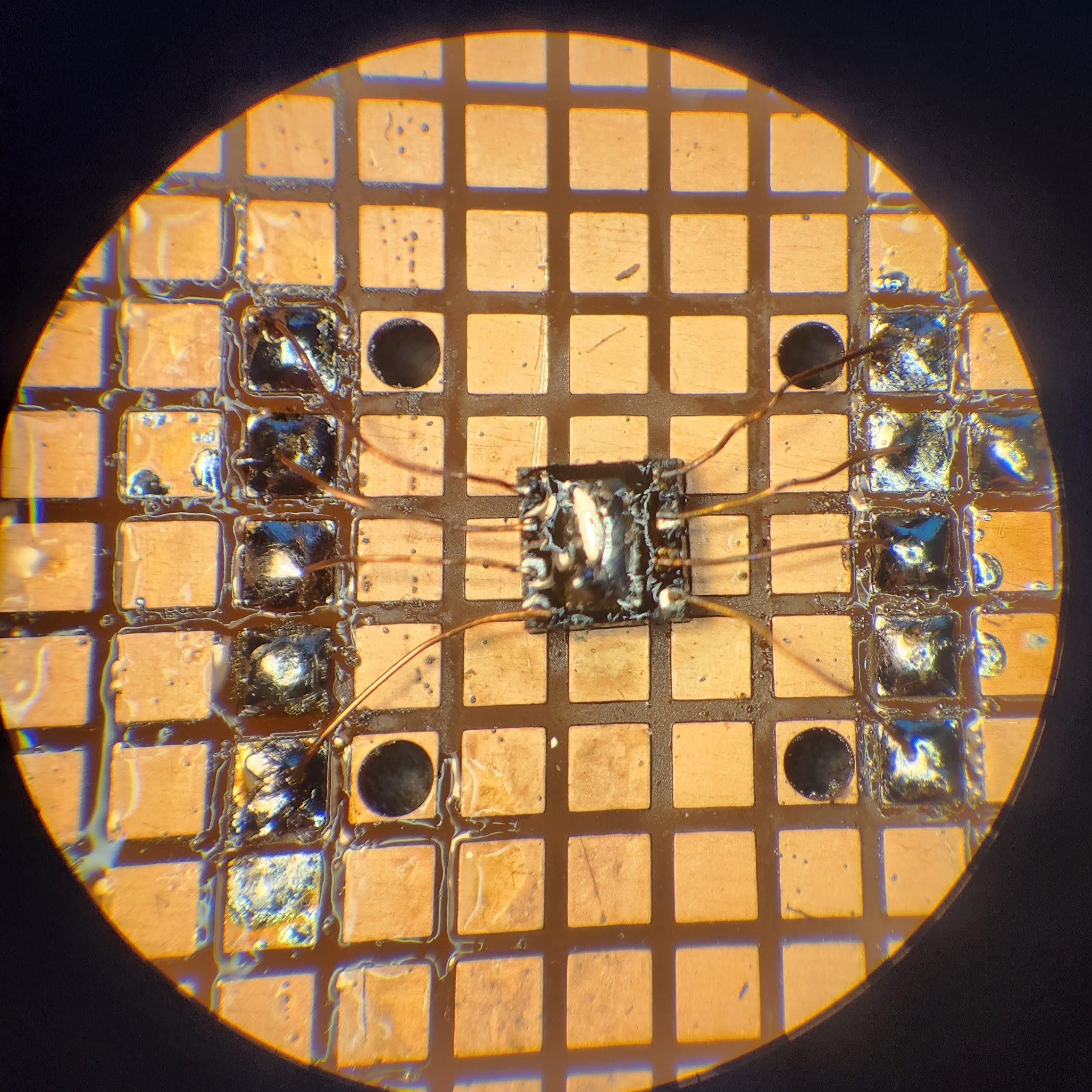
    This was supposed to just be another IC and a few passives. Instead, I ended up dead-bugging a chip measuring 1.5mm x 1.5mm. With the hope of troubleshooting the circuit directly.

    Yep. Check out the picture below. It really did feel like wire bonding!


    The copper wires are once again the strands from those cheap jumper cables. They are super thin and readily accessible. Unlike magnet wire, they don't have any insulation on them which I like. It means that I don't have to mess around burning varnish and the crust that comes with it. There isn't really much of a danger of shorts either, the wire is so thin that you can just route it around in midair and it stays put.

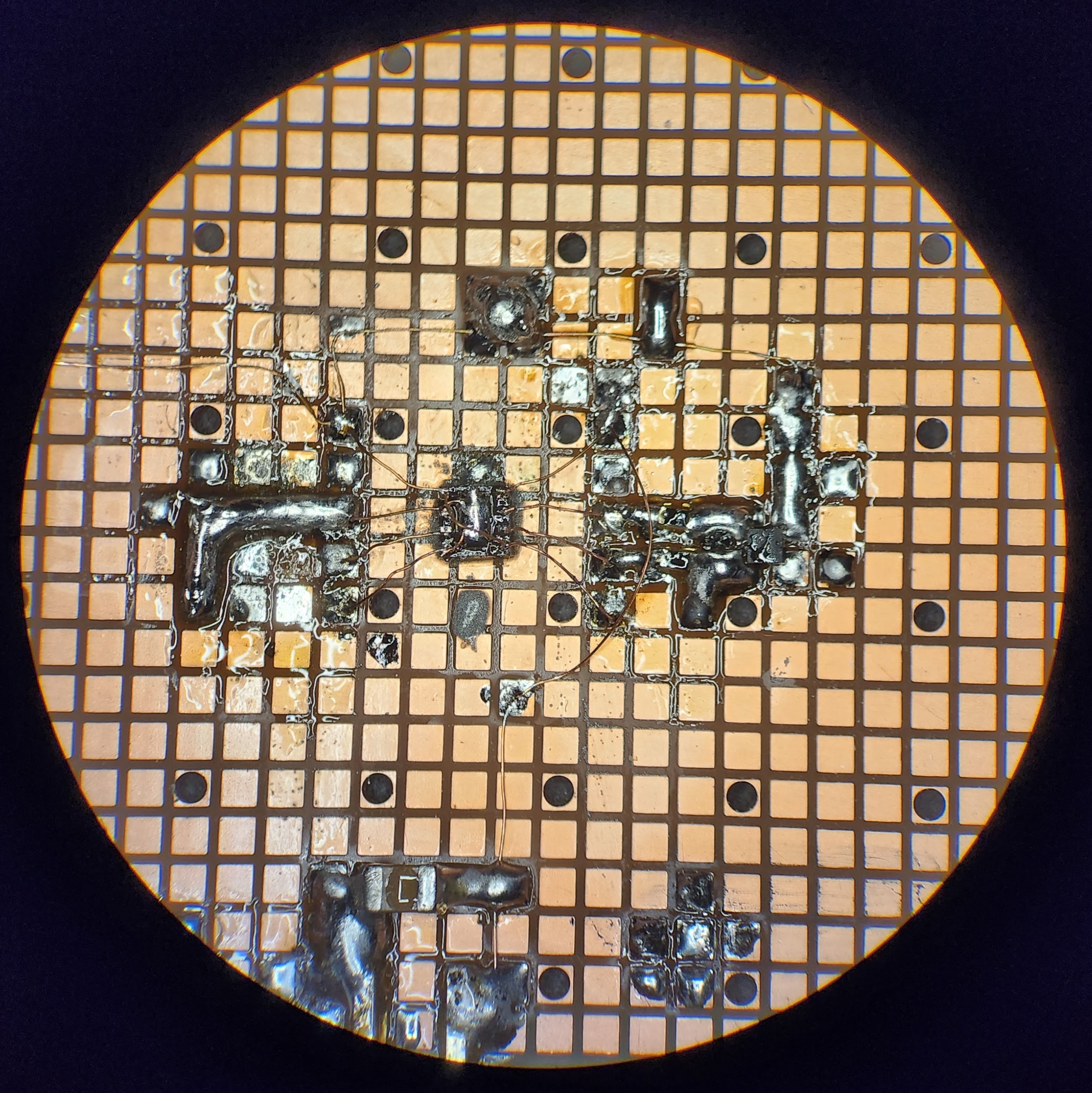
    Here is a partial picture of the completed circuit. After the strong start with just the chip I was a little disappointed I couldn't do a better job on the rest of the circuit but I didn't have all night...

    The fun part is that circuit did in fact work. I measured almost 100 mA flowing into the battery when I plugged it in! With the circuit working my next plan was to start messing around with diodes and dummy loads and what not and use this as my test bench.


    After sleeping on it (and asking a smarter friend) I realized that would be a dumb idea. The diode really shouldn't have anything to do with it so there must be another issue.


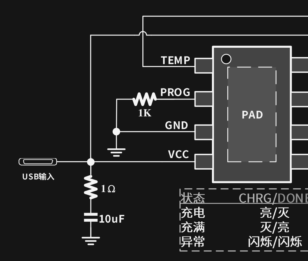
    It occurred to me that I didn't actually put a 1 Ohm stabilizing resistor or a 10 uF capacitor on the input. I figured the traces on the board would be high enough resistance to replace the 1 Ohm and that the capacitance already on the 5V bus would be good enough that I could just slap down a 4.7 uF cap and call it a day.


    Well after messing around with the capacitors close to the charging IC and observing some interesting and inconsistent behavior I realized that those components were probably included in the datasheet for a reason!

    So instead of messing around with my crappy dead-bugged circuit I chose to just bodge the proper capacitors and resistor onto my test-board directly.

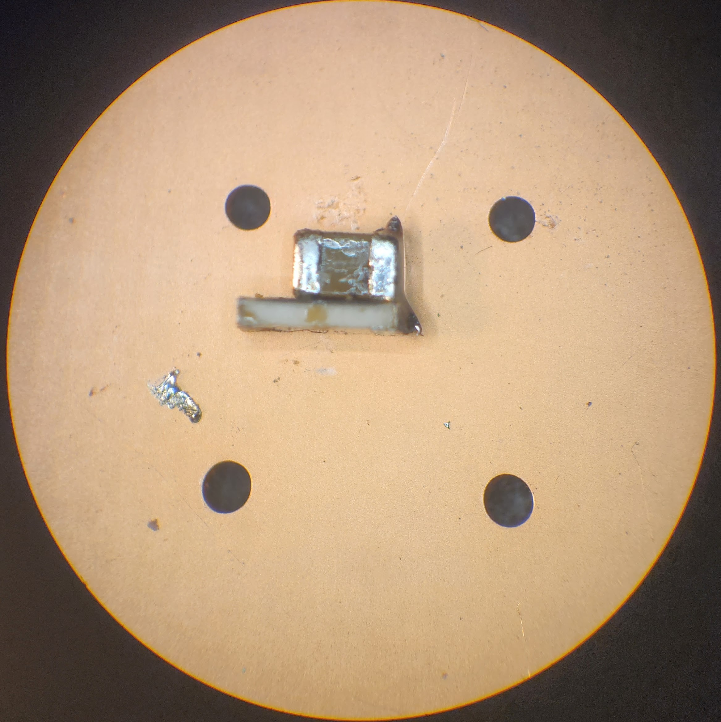
    First I stacked a resistor and capacitor on top of each other and soldered their two ends together. The rest was just some time with some very very thin wire and the microscope.

    The solution to my charing woes!
    Remember, datasheets give you example circuits for a reason.


    SUCCESS!


    This is probably my favorite bodge I have made to the CRAPi board so far just because it's sort of cool to look at. You can see that I added the recommended capacitance to the battery input as well as the recommended capacitance and resistance to the VCC of the charging IC.


    Sure enough, after making this addition to the circuit the battery charged up all the way no problem, even with the diode. That leads me to think that there was just some weird instability or oscillation that was happen in the charging IC. This particular IC also has a trickle charge mode that attempts to revive dead batteries with < 1 mA charging currents if it detects an under-volted battery. I suspect that this has something to do with the problem as well, but without the time to stick the problematic circuit on a scope I won't know for sure. Oh well!


    Sometimes you just have to move on.

    Next steps.

    This was pretty much the final technical issue with this version of the CRAPi board. I've already updated the Rev. 3 PCB to include more capacitance and the (apparently) very important stabilizing resistor. I am nearly done updating the silkscreen to clearer and more descriptive of the "hidden features" of the  CRAPi board. 

    I've also...

    Read more »

  • Rev. 3 in Progress

    Chris09/10/2023 at 05:28 0 comments

    This is was going to be a way more in depth post about Rev. 3 updates but then my laptop died and nothing saved so I guess I will just type up a quick version for now.


    There are a few main things that I need to change in Rev. 3. The biggest issue so far is that the battery charge never charges the battery fully. It only gets to 3.9 V. After some thinking and some tinkering I figured out the problem, and this was a great learning moment!

    Battery Charging Woes

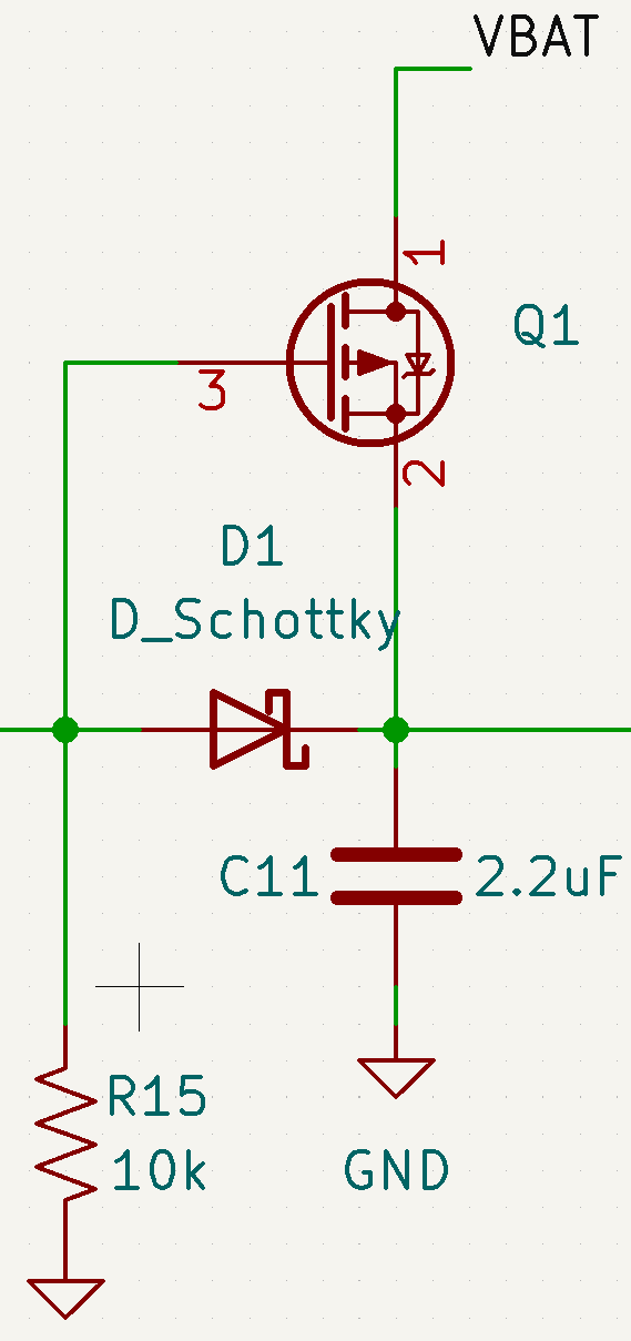
    To handle the power switching between USB and battery, I threw a diode in front of the battery. That way VIN wouldn't go to the battery directly but when USB wasn't connected it would be the battery powering the system via the linear regulator. The problem?

    What happens when the battery is no longer the path of least resistance.

    That's right, at a certain point in the charging the diode became the preferential current path meaning the battery never increased fully charged. After looking at the data sheet for the diode it worked out to a forward drop equivalent to about 2 Ohms. The fact that the impedance of the battery was high than 2 Ohms seemed strange to me but thinking about the crappy contacts and connectors it made sense.

    I was able to confirm this theory but removing the diode and letting the battery charge up. Sure enough, that worked! I got the green light!

    Green Light baby!

    The battery charging solution

    I poked around a little bit and realized that I just need to stop being lazy. The more correct way to handle this power off is with a P-FET and resistor.

    The idea here is that the P-FET acts like a Normally Closed switch. It will happily conduct until you hook up a VIN that pulls the gate higher than the source (P-FET are weird) and the P-FET opens, protecting the battery. I think this is something called an "ideal diode" configuration, or something like that.

    Anyway! Figuring this out was honestly the easy part. The hard part was

    1. Integrating ANOTHER chip and resistor onto this board.

    2. Finding a small, cheap, and least crappy P-FET I could find.

    In this case the "crappiness" is defined as the On Resistance of the FET. This parameter was especially important to me because when running on battery power you are running all the current through the FET. So if there is a super high on resistance that is basically just burning power.


    Assuming an average current draw of 10 mA (just to make the math easy), using a diode in the configuration above gives a drop of about 2 Ohms.  I managed to find a P-FET for cheaper than the diode with an on resistance of just 100 milliohms! Now we are talking!


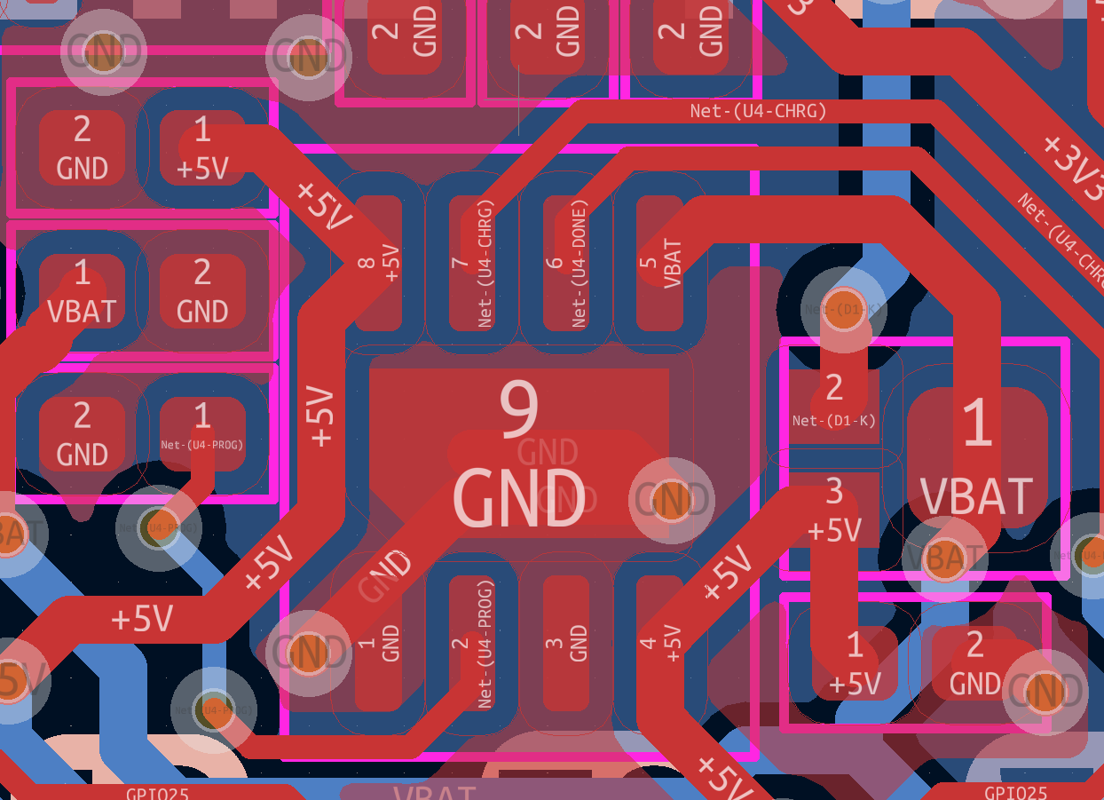
    The next hardest part was just integrating it into the board! Thankfully I managed to do it without too much frustration. You can see the P-FET and extra resistor on the right hand side of the image below. This thing is TINY. Just 1.3mm by 1mm! What a time to be alive!

    That's all for now. Slowly I am moving towards Rev. 3! Like I've mentioned before, I will be trying PCBWay for the next round of boards and I am super excited to get some more microscope pictures!

  • Rev. 2 - LiPo Current Testing and Questions

    Chris08/16/2023 at 16:20 0 comments

    Just a quick log today.  The last log had me checking my biggest "creeped" feature, as it were: the LiPo Charger.

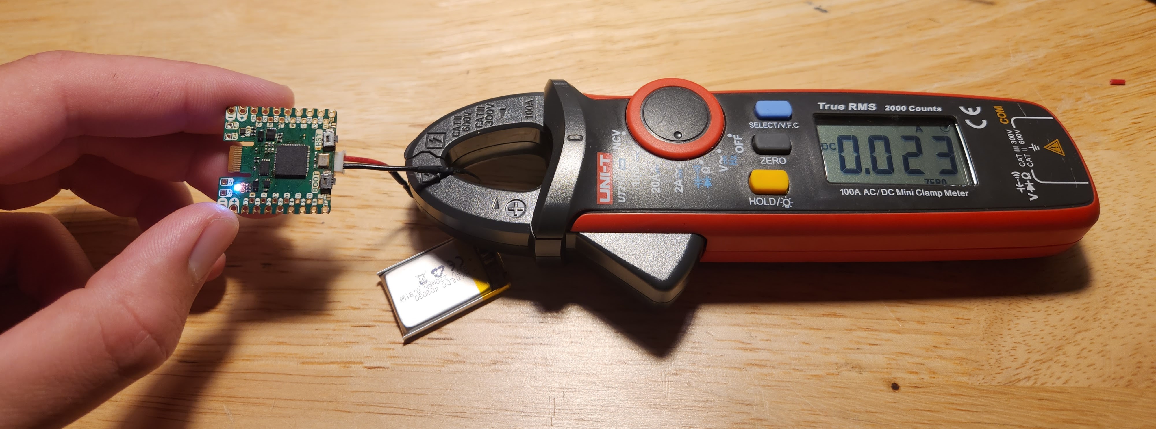
    I bought a less sketchy LiPo cell and borrowed a suitably accurate clamp meter from a friend.

    Don't let labeling on the meter fool you! The firmware on the meter had been reconfigured to measure 6000 counts rather than 2000. Considering that the charging IC was configured for 100 mA charge rate I would call this a win!

    This setup is also convenient for power draw measuring too. Sitting idle with an install of CircuitPython and with the R, G and B LEDs turned on, current draw measured anywhere from ~25 mA to ~35 mA, which seems to be in the ball park for the RP2040. Eventually I would like some more power logging / bench marking.

    I also wanted to look into an issue that I mentioned in my last log. 

    For some reason, if you unplug the USB cable while charging the battery, and then try to immediately plug it back in, the charger does not respond: no indicator light and no current flow. If I wait for a while, running off battery power (so no power cycle) and try plugging in the USB again, then it will charge as normal.  

    I know that these chargers can normally have some sort of hysteresis but  1+ minute seems a little strange. I am wondering if the Schottky is messing with the LiPo charger some how... maybe I should investigate a more graceful switching option for Rev. 3 of the board.

    If anyone has any ideas for this issue I would love to hear your input!

  • LiPo Charging - First Try!

    Chris08/14/2023 at 03:13 0 comments

    The last log on Rev. 2 got a bit into the weeds. That's my bad. Another product of my late night brain but hopefully you got the gist... These posts always take way longer than I think to write because I keep thinking of things I want to include!


    Anyway, hopefully this log will be less rambly because today I tested out the last core feature of the CRAPi2040 board: LiPo Charging.

    Spoiler: I nailed it first try :D

    Nothing ever works first try so this is sort of a big deal for me.


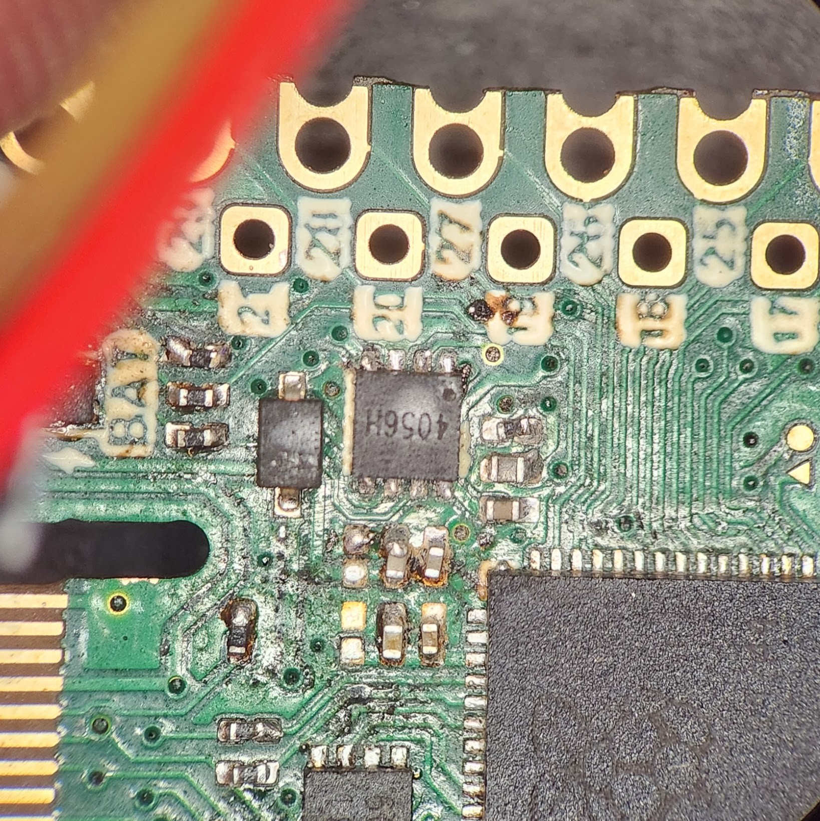
    Here's an up close, but crusty, shot of the LiPo circuity. Sorry about that.

     I was pretty deliberate in the choice in my charging IC. I had two primary criteria:

    • Small as possible
    • Constant Current and Constant Voltage Charging.

    This random chip that I picked from LCSC does both of those things... Well, I am 100% it does the "being small" part well. Only about 80% sure on the CC feature as the entire sheet was in Chinese and the PDF translation on Google refused to work for some reason. I got around that by using that cool live camera translation thing on my phone.

    As a side note, this was my first experience with LCSC and it definitely has it's uses. If you can fill in the blanks in some of the translations you can find some really niche stuff. The main reason I went to LCSC is because Digikey didn't have any appropriately minuscule LiPo charging ICs. The shipping was reasonable too considering it's an ocean away. If you are looking for something very particular and haven't already, checkout LCSC!

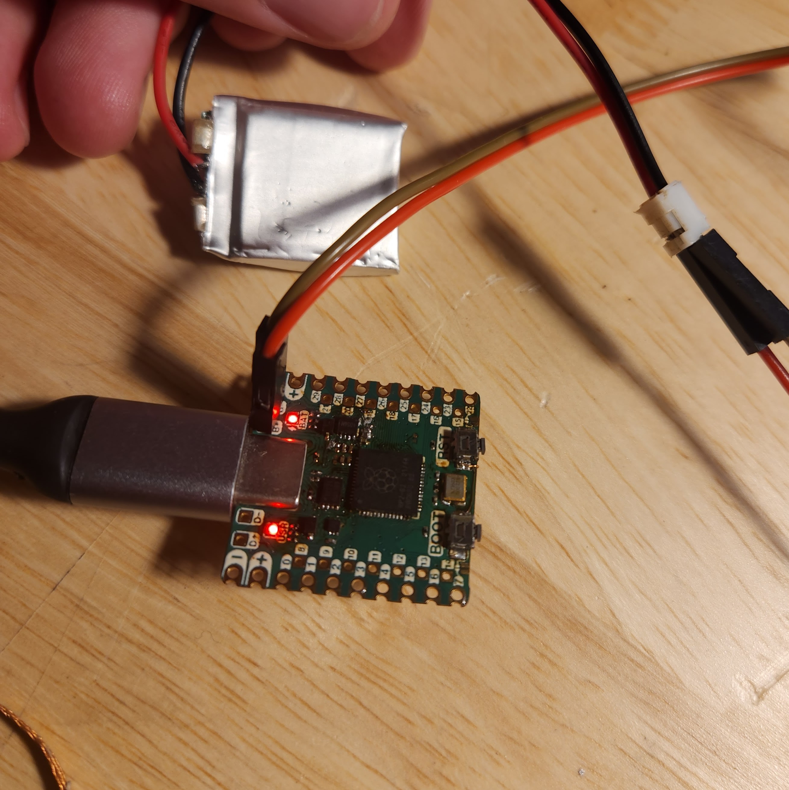
    Here's the picture of success that made my day!


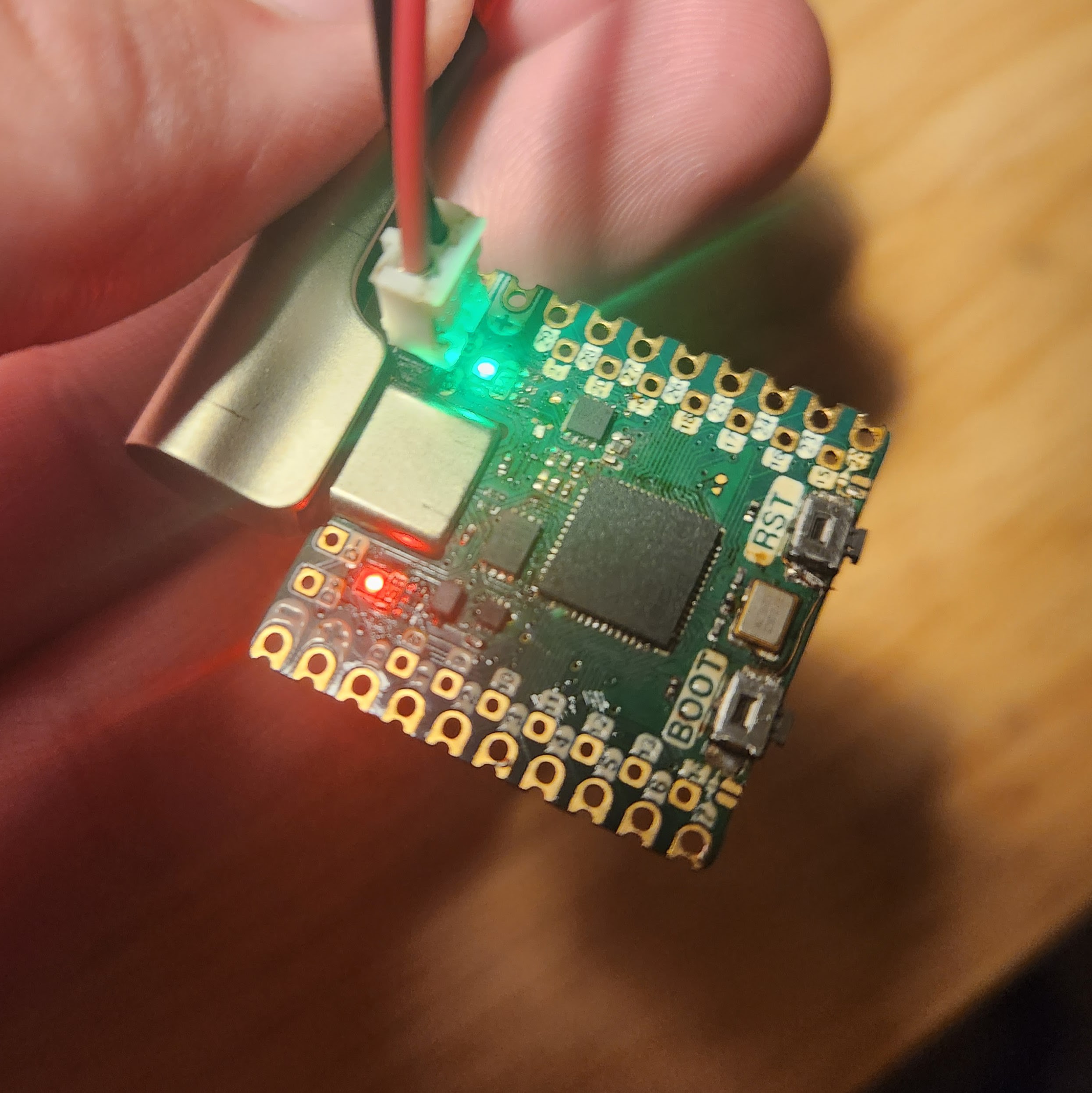
    Look at those two beautiful RED LEDS!


    The first red LED is the power but the second red LED is the charging indicator!! The bad boy popped right on the second I hooked up that beat up LiPo. Also, if it wasn't clear. That second LED (labeled as BAT), is RGB. The R and the G is hooked as the status LED for charing and the B is hooked up to pin 25 so that code meant to run on the Raspberry Pi Pico will port over well.

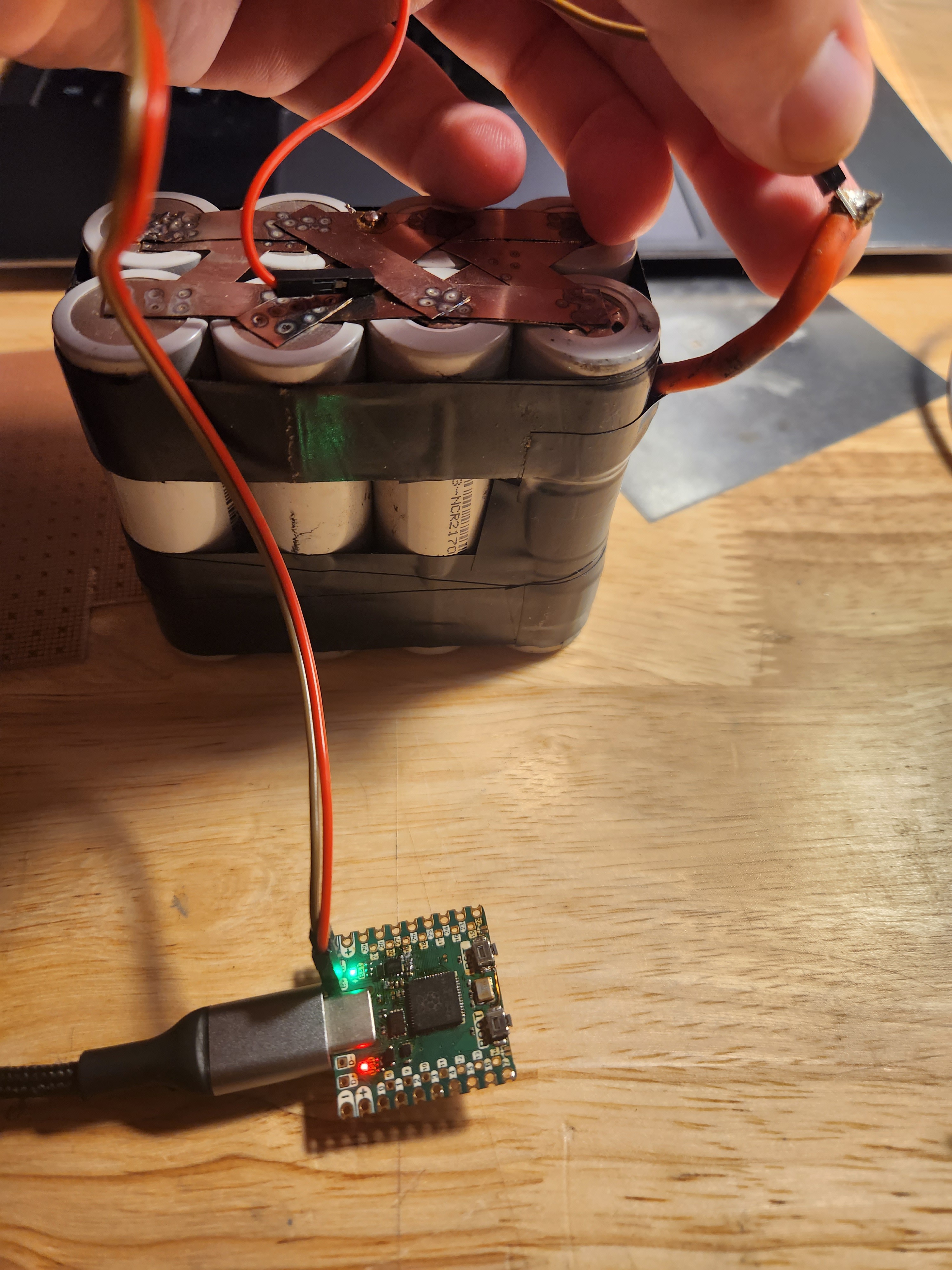
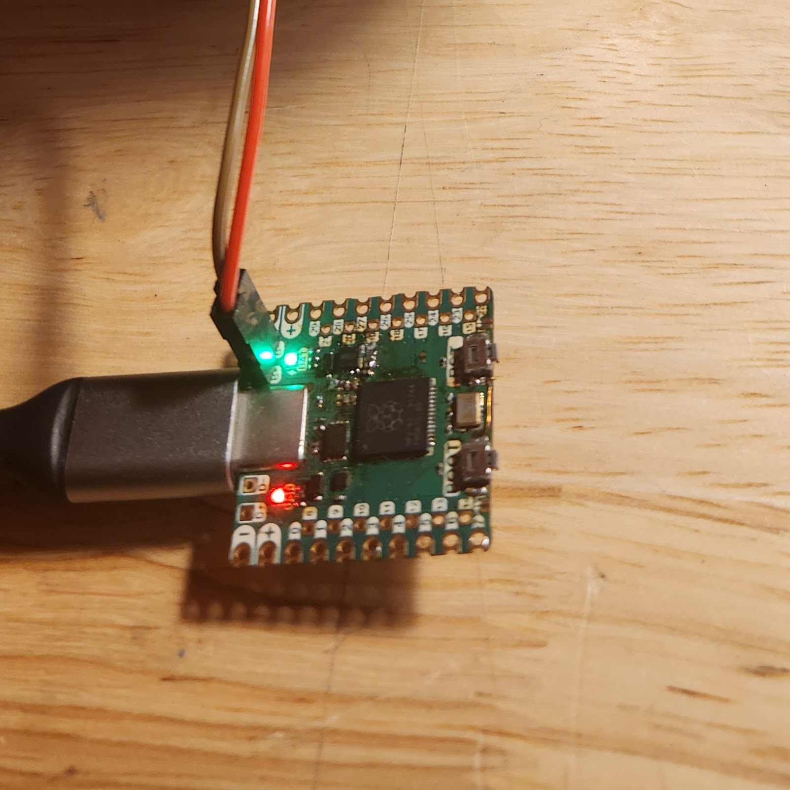
     I wasn't patient enough to let scary LiPo try to charge all the way, so I jammed some jumpers onto some batteries that were already fully charged to see if I could get that green LED to show it's face.

    And there it is! YES. AMAZING. That feels so good. And by the way, this is only a 1 cell charger. The connection above is just testing one set of batteries in a 2S4P string.

    Green Green Green Baby!

    This also shows off one of the changes that I made to the Thads in Rev. 2 that I don't think I have mentioned yet. On Rev. 1 of the CRAPi board I had these really really tiny plated through holes which probably were sort of useless for getting solder to flow through.

    In the second revision of the board. I made the holes way bigger. This is for two reasons:

    • It will probably help when soldering the Thads to other boards
    • AND they are the perfect size for those bread board jumpers that everyone uses.

    The picture below sort of shows what I am talking about from the bottom view. The holes are just just tight enough to use as a friction fit but that's probably a bad idea. Also note the 0.1 inch spacing!

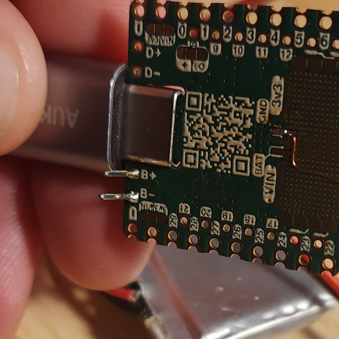
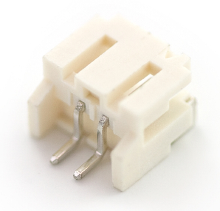
    In all of this excitement I almost forgot to test another feature that I labored over in Rev. 2 on the ProtoGrid. I succeeded in jamming a (somewhat hidden) right angle JST connector footprint onto the CRAPi board! You know, this one:

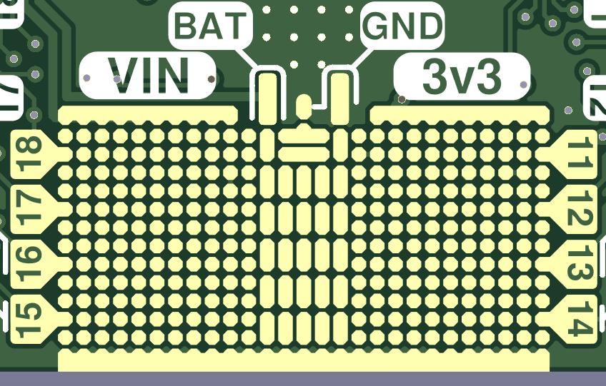
    Direct your attention to the BAT and GND labels. Those aren't just for show! Those skinny little pads are basically the exact same width as the leads of the JST-PH connector shown above. Obviously, I didn't have much room to work with so I wasn't sure if this would even work.

    Again, to my surprise: the footprint worked perfectly. The front anchor tabs of the connector have no problem being soldered down to the GND rail at the bottom of the ProtoGrid. I'm pretty sure I was designing this on a train to Chicago in the middle of the night. So, I don't really remember designing this, but I am glad it worked...
    Read more »

  • Rev. 2 Assembly and Blinking!

    Chris08/11/2023 at 03:39 0 comments

    Previously, we took a look at some gorgeous ENIG plating, clever silk screening, and a USB-C connector that consisted only of the 0.6mm PCB substrate that the rest of CRAPi board lives on. Honestly, I almost didn't even want to put the boards together. Seeing them come out so well made my week! The thing is, this isn't my first rodeo, I know how these things go.

    Here I am feeling like a smarty pants with some shiny boards and cute little components, but I already know that this isn't going to work on the first try... but we must push on! The only way to turn the unknown unknowns into known unknowns, and eventually into known knowns is to just slap a board together and pretend that everything will work on the first try.


    Now if I was smart, I would assemble the board bit by bit, ensuring that each component is soldered down and working as intended. If I was this hypothetically smart engineer, I would test my board by assembling things in the following order:

    1. Linear Regulator
      Rule No. 0 of Electrical Engineering: Make sure it's plugged in.
    2. Processor
      Once the heart is beating, gotta make sure the brain is thinking
    3. Flash
      Once the brain is thinking gotta make sure the brain is remembering
    4. Everything Else
      Everything else is really just a bonus to me...

    So with this plan in mind. I am going to completely ignore it and just put the board together all at once and hope for the best! Sometimes being smart and optimistic is mutually exclusive, and there's nothing you can do to stop me!

    Assembly!

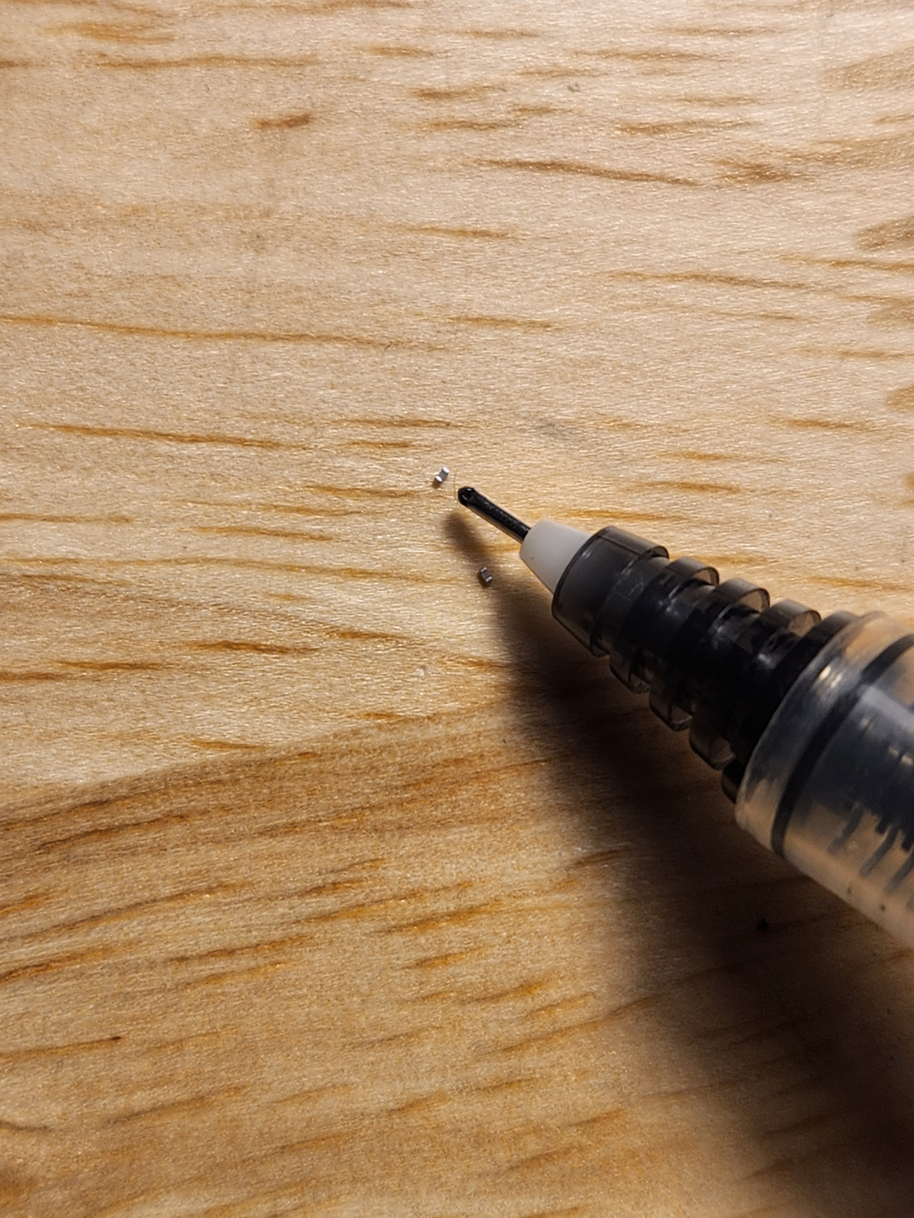
    I mentioned it in the last post, but one of the changes between Rev. 1 and Rev. 2 was the move from 0402 components to 0201 components. In my head I knew that 0201 components were half the size of what I had gotten used to on Rev 1, but its a totally different thing to actually see how tiny these things are.


    I mean look at this! Look how dumb and tiny they are! That's the tip of a pen! Man that was intimidating. I tried my best to only remove the number of components that I needed from the tape, but of course a few extras popped out now and again. It literally felt like brushing sand off my desk, if I felt it at all. At least clean up is easy. Just need to vacuum it up with the rest of the dust on my floor!


    Once I got over the grains of sand that I would be trying to work with, it actually wasn't too hard. I had a pretty nice pair of tweezers and my eye sight is decent so populating and positioning those itty bitty Rs and Cs wasn't much harder than with 0402 components.

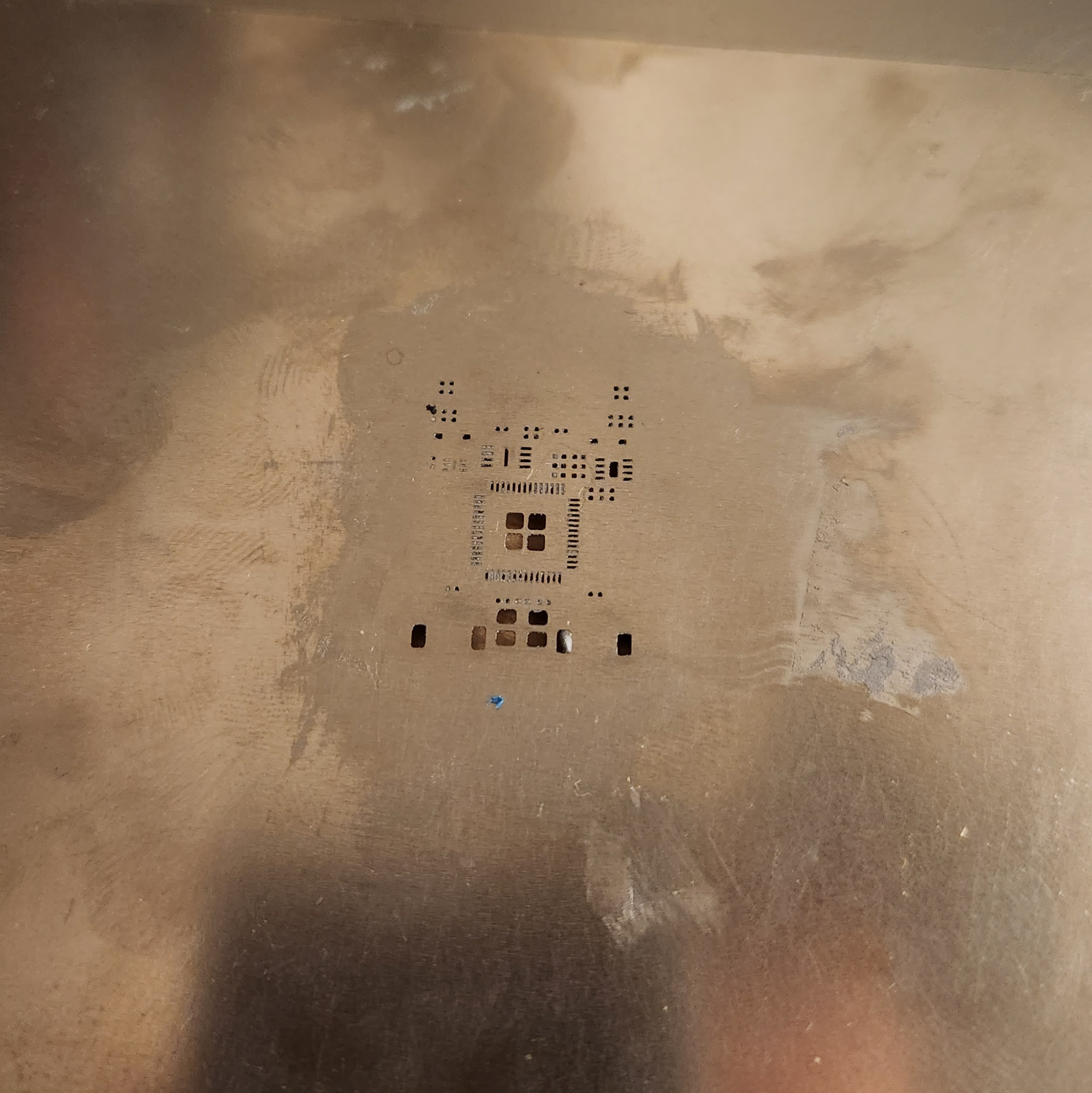
    Armed with my solder stencil and paste, I lined everything up the best I could and gave it a good swipe to make sure that I got all the pads covered.

    I carefully placed all the components into their respective locations yadda yadda, threw that thing on my crappy hot plate and watched the magic happen

    Assembly Problem #1 - Solder Paste Trouble.

     I mentioned that my cheap little hot plate gave me some problems in the last post and that I managed to mitigate them by heating up the hot plate with the PCB already placed on top. I did not have such luck with this new problem.

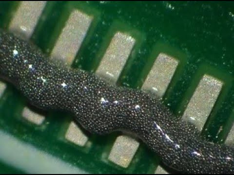
    In case you have never seen it up close before, heres a random picture from the internet. Ypi can see that solder paste is just tiny balls of solder in a suspension of flux. Of course, the flux is supposed to melt first, and in the process clean the metal joint of oxidation that would prevent the solder from properly wicking on to the joint and mating the two surfaces

    The interesting problem that I was experiencing is that the flux bubbling and boiling under my components created enough force to knock around the 0201 components. Because the flux melts before the solder does, there is nothing to hold those little grains of sand in place while the flux does its thing.

    Eventually I'll look into the problem; obviously this has been solved.For now though, I don't really care!. Instead of mucking around with different types of solder paste or throwing down a few Alexander Hamiltons...

    Read more »

  • Rev. 2 has arrived (and it works!)

    Chris08/09/2023 at 03:59 0 comments

    In the last log we suffered through the very first revision of the CRAPi board! That whole experience really lived up to this board's namesake. Not surprised, just disappointed. The first two logs were retrospectives. Rather than just jumping into where the project is now I wanted to make sure I showed the last few months of design and trouble shooting. The board became more and more unreliable until it eventually refused to enter programming mode. Making stuff is hard!

    Thankfully, this post now brings us firmly into the present. I had decided to cut my losses with Rev. 1 and focus on moving forward. I started Rev. 2 in the middle of February and  "finished" the design around the middle of July, with time spent on the project ramping up exponentially once the semester was over. All told that's about 5 months worth of work. So here's what changed in that time:

    Changes in Rev 2. of the CRAPi2040

    • Pin Labeling
      • Went back to traditional silkscreen but used a "knock-out," negative-space style.
    • Improvements to the ProtoGrid
      • Pin pads that should let solder bridges form more easily
      • Better GPIO Access
      • Vertically oriented pads for 20 mil spaced surface mount connectors
      • More prototyping space.
    • Thad Improvements
      • Increased the diameter of the center hole to match diameter of common jumper wire
      • Bread board jumpers can now be (hopefully) friction fit into the Thads and/or soldered
    • Right Angled buttons
      • Low profile buttons hang off the side of the PCB
      • Allows for boot mode and resetting even when the board is upside down
    • Route-able Power Pins
      • Solder jumpers let you route 3.3V or VIN to either side of the board
      • Independent of each other - 4 total configurations for max flexibility
    • Configurable Power LED
      • Lets you reclaim the red power-on LED for RGB usage
    • A second BLUE LED attached to Pin 25
      • Blue LED attached to GPIO 25, so default Pico blink examples are (almost) drop in.
    • RESET and BOOT button breakout jumpers
      • Solder jumpers to route the BOOT and RESET buttons to GPIO pads.
      • Gives an optional, general purpose user button (which seems to be pretty rare!)
      • Can reset itself (which I guess could be useful!)
    • Castellated Holes
      • Allows for use on a breadboard and as a module on a PCB
      • No components on the back of the board so no cut out needed.
    • QR Code Link to Documentation
      • Quick access to pinout documentation because those labels are tiny!
    • LiPo Battery Charging IC (!!!!!!!!!!!)
      • Single cell LiPo battery charge and automatic switching circuity.
      • On board indicator of charging status via a second RGB LED.
      • Oh god why did I decide to add another IC to this design.

    How's that for 5 months worth of work?

    With all these changes it also meant that I needed to start routing completely from scratch. This time I decided to drop the trace width from 7 mil to 5 mil as well as the size of the vias. Just for my own sanity I also changed all the passive components on the board from 0402 to 0201. Some may argue that this was just exchanging sanity in the virtual world for insanity in the real world went I went to assemble the things.

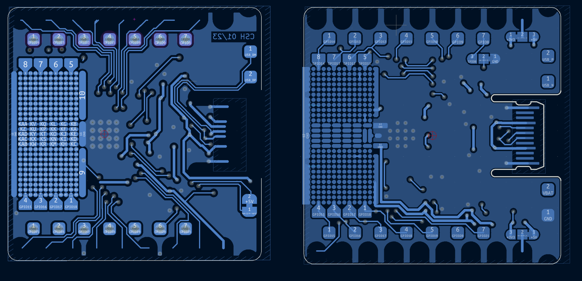
    Routing Comparison

    All in all I'd say that I did a much better job routing this time around. My main focus was keeping traces on the top layer of the board and ground plane in tact on the bottom of the board. Just for fun I also made sure that to length match the traces going to the flash chip and the USB lines, mostly because I like how the squiggly lines look. Rev. 1 is on the left and Rev. 2 is on the right. Not bad right?

    Again, old on the right, new on the left. It gives you a pretty good idea how things changed and why it took 5 months to Rev the board!
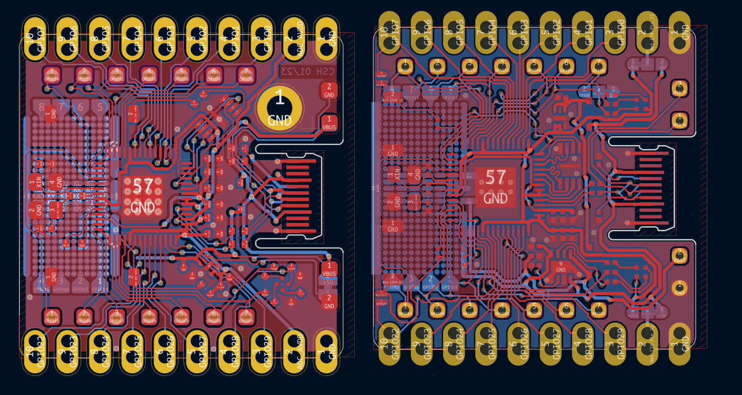
    You can also see that I had to give up the mounting hole... I determined that all the new features would be worth give it up. The board doesn't have any components on the back side so you can always double side tape it down. I am also thinking about making some sort of carrier board that would solder to the Thads specifically to add mounting holes. So many ideas so little time.
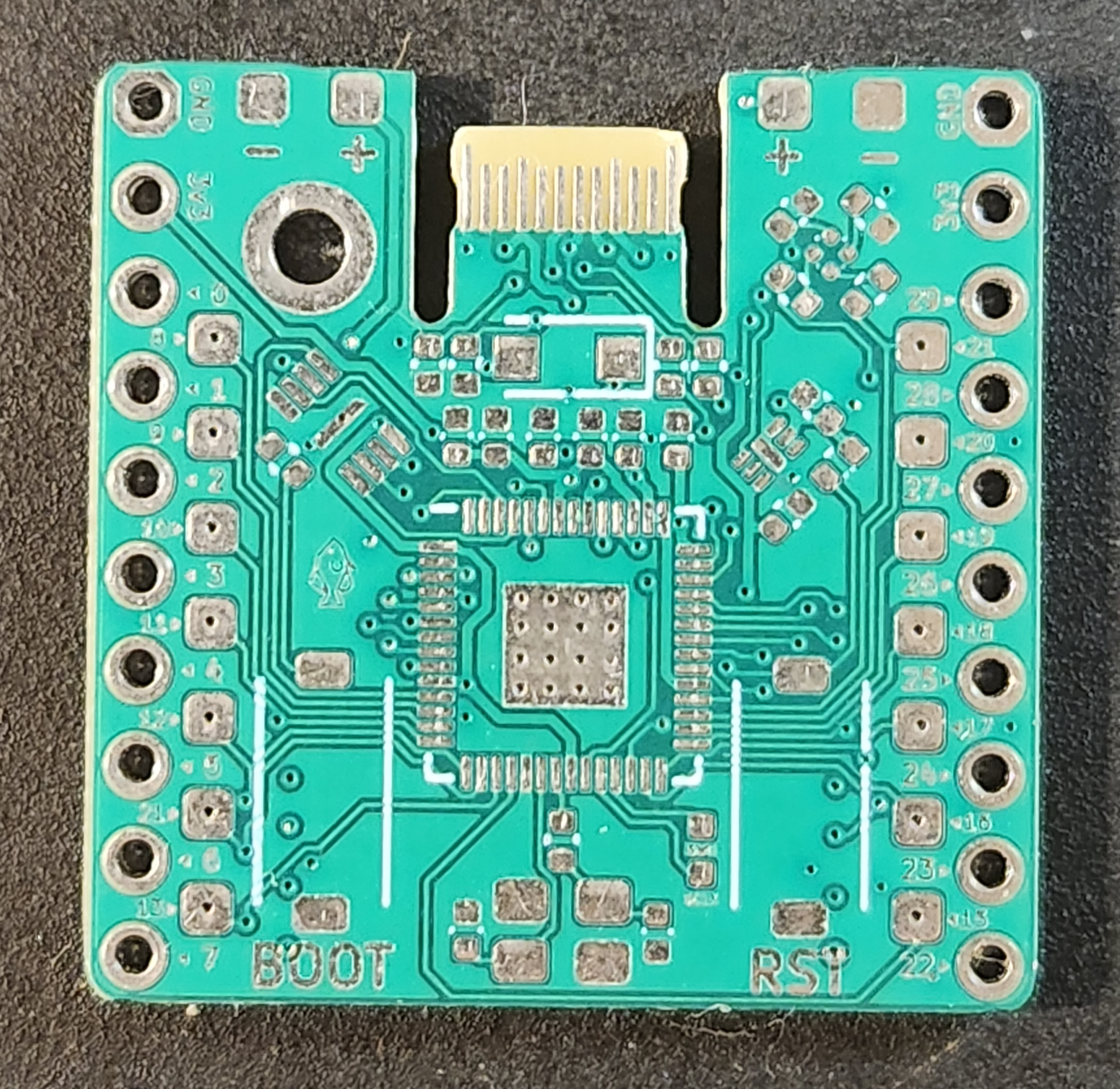
    Cool...
    Read more »

  • Rev 1. PCB Assembly!

    Chris08/08/2023 at 04:34 0 comments

    Alright here we go! In case you missed the last log, here it is! Check it out because what you're about to see will make a lot more sense. Just like the last log, this log is going to be a retrospective, but I promise that the next CRAPi2040 log to grace your retinas will be firmly rooted in the present!

    We left off with the very first "completed" revision of the CRAPi2040 board. All told it probably took a few tens of hours to design and layout. Some of that time included picking out parts, learning KiCAD, and looking up reference material. But I would say that 75% of that time was for sure spent routing and rerouting traces and trying to keep my ground plane in tact. I'm going to be honest, the amount of time I spent laboring over that routing was probably not healthy considering I was supposed to be taking a break from school and only focusing on work and my friends and family.


    But who cares about all that stuff. You're here to see that gorgeous board! So here it is!

    Front of the CRAPi2040 Rev 1.
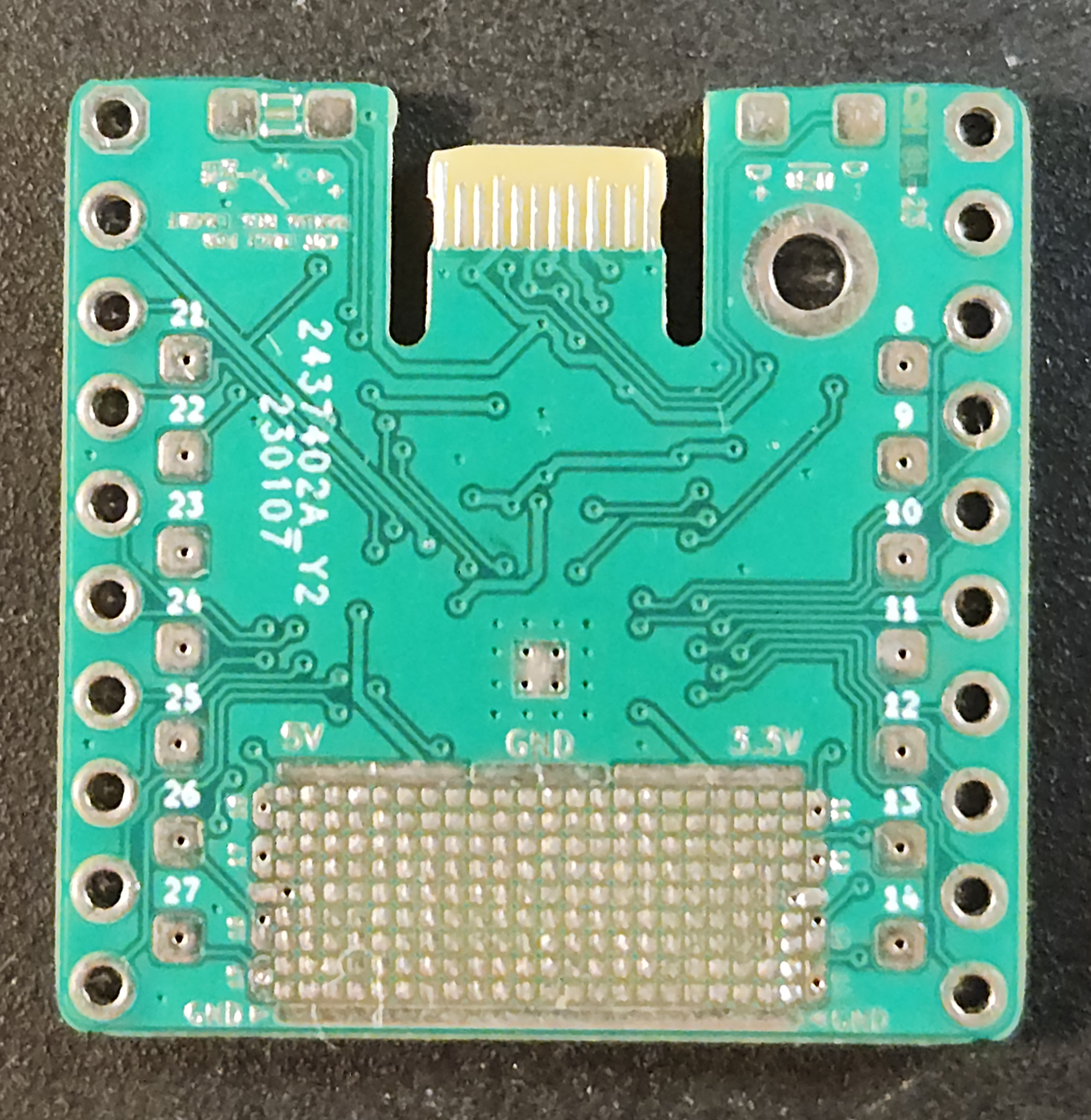
    Back of the CRAPi2040 Rev. 1


    Beautiful I know, even if my phone camera washed it out a little. You can get a really good look at the routing thought which I think is awesome. You'll notice that I didn't do a great job at keeping my traces on the top of the board so some current paths are probably longer than they need to but on a board that is only 1 square inch probably not a huge deal. To be honest, it looks a little crappy to me but hey sometimes you've just got to send it. The gerber files that is, to JLCPCB.


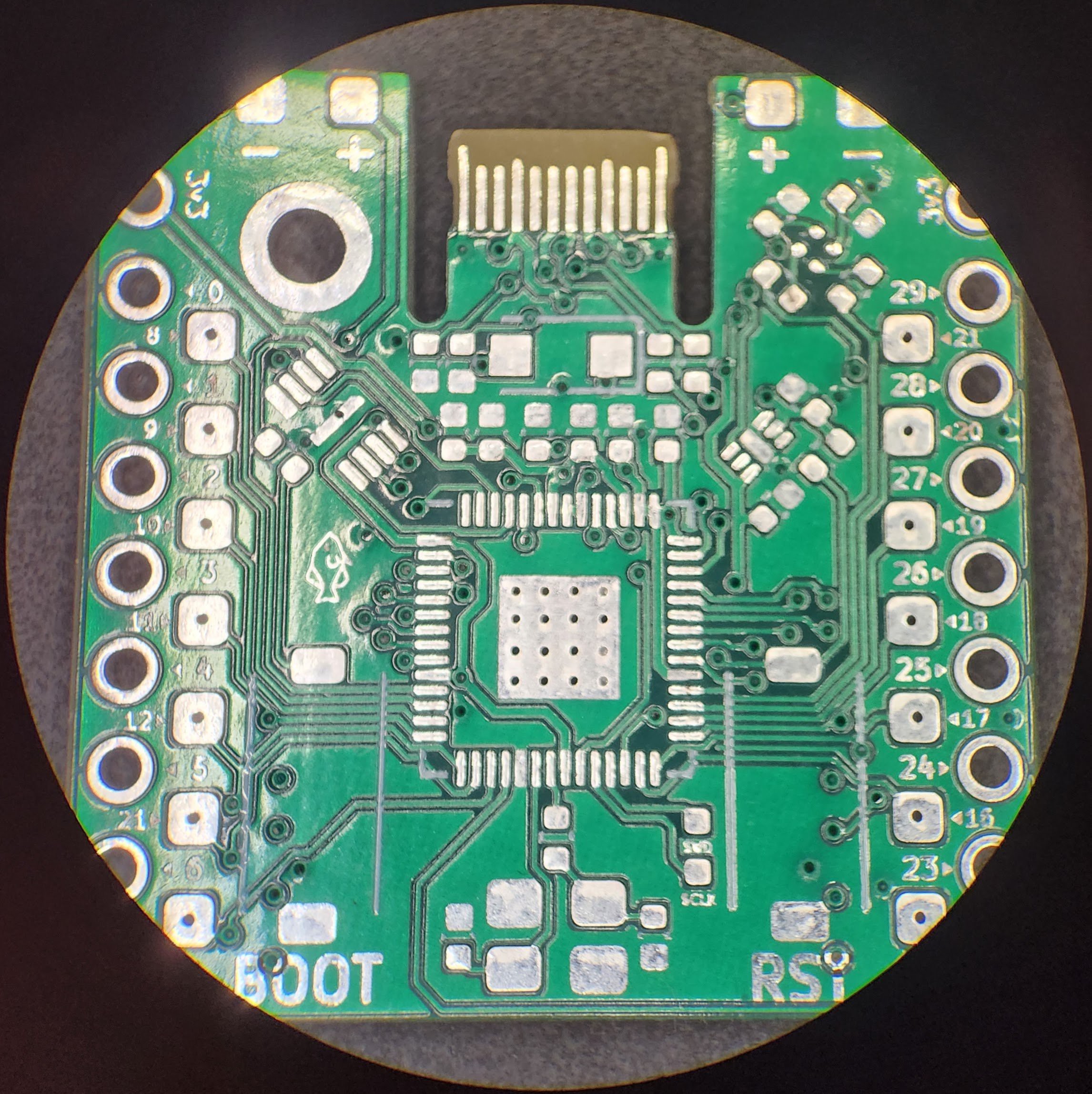
    If those pictures don't satisfy you, say no more. I am lucky enough to be the proud owner of a garbage bin microscope! It's sort of hard to take good pictures with my phone through a microscope but it's better than nothing. Plus it's a huge help when trying to deal 0402 components. My eye sight is pretty good but this really takes a lot of the guess work out soldering these leadless components. To the surprise of no one, it's hardly smooth sailing from here so I'll take every advantage that I can get.

    Front Microscope Shot of Rev. 1

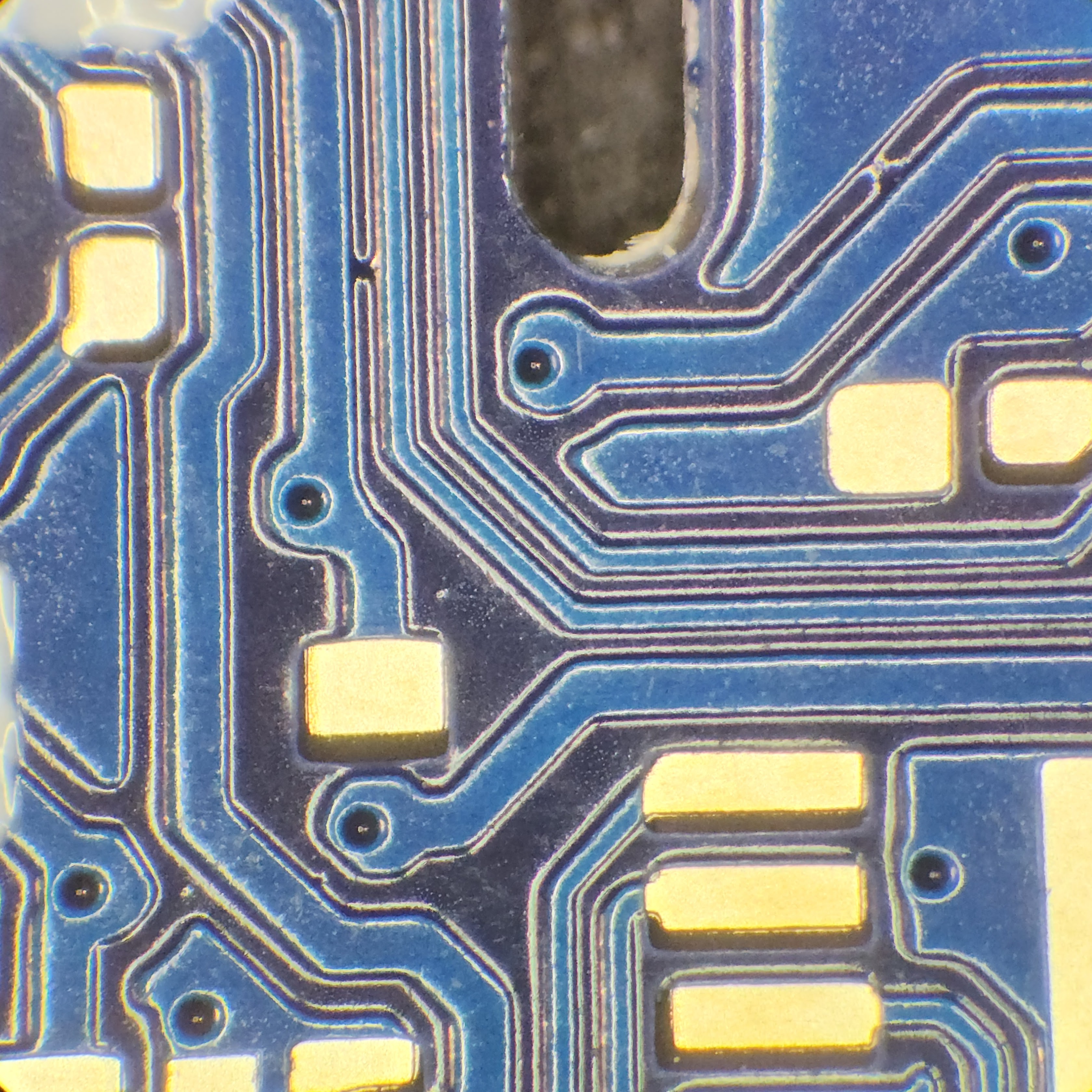
    At a first glance under the microscope things look GREAT. I didn't really know what to expect from JLCPCB because these boards were literally 20 cents each. The driving factor for such a low cost board, as you may have noticed, is that I went with a HASL finish on the copper pads. This was my first time even hearing about the process so I needed to look into it.

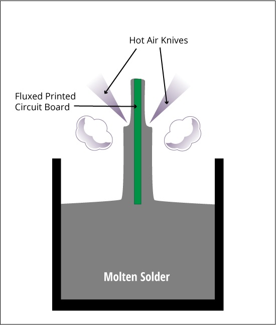
    HASL stands for Hot Air Solder Leveling and the process basically involves dipping the entire circuit board into a vat of molten solder to tin the exposed copper. As the board is withdrawn all the excess solder is blown away by hot air knives. Or so I am told by Google. Looking at picture definitely helped.


    HASL Surface Finish

    This is opposed to the typical ENIG (Electroless Nickel Immersion Gold) process that most "normal" PCBs are put through. This is the one that gives you those nice shiny gold pads. The ENIG process deposits a layer of nickel and then a layer of gold on to all the exposed copper, without using an electric current. Nickel is essential for preventing the gold from diffusing into the copper and of course the gold is great to solder to and provides corrosion resistance. But obvisouly the most important part is that ENIG is prettyyyy.

    Resulting Layer from ENIG ProcessThe (G) stands for (G)old so it's cleare why ENIG would cost more money than HASL. When I sent the boards away I already knew that I was going to need to do another board revision so I didn't bother getting the good stuff. That turned out to be a great choice considering all the issues these boards would have. I'm not surprised, just disappointed.
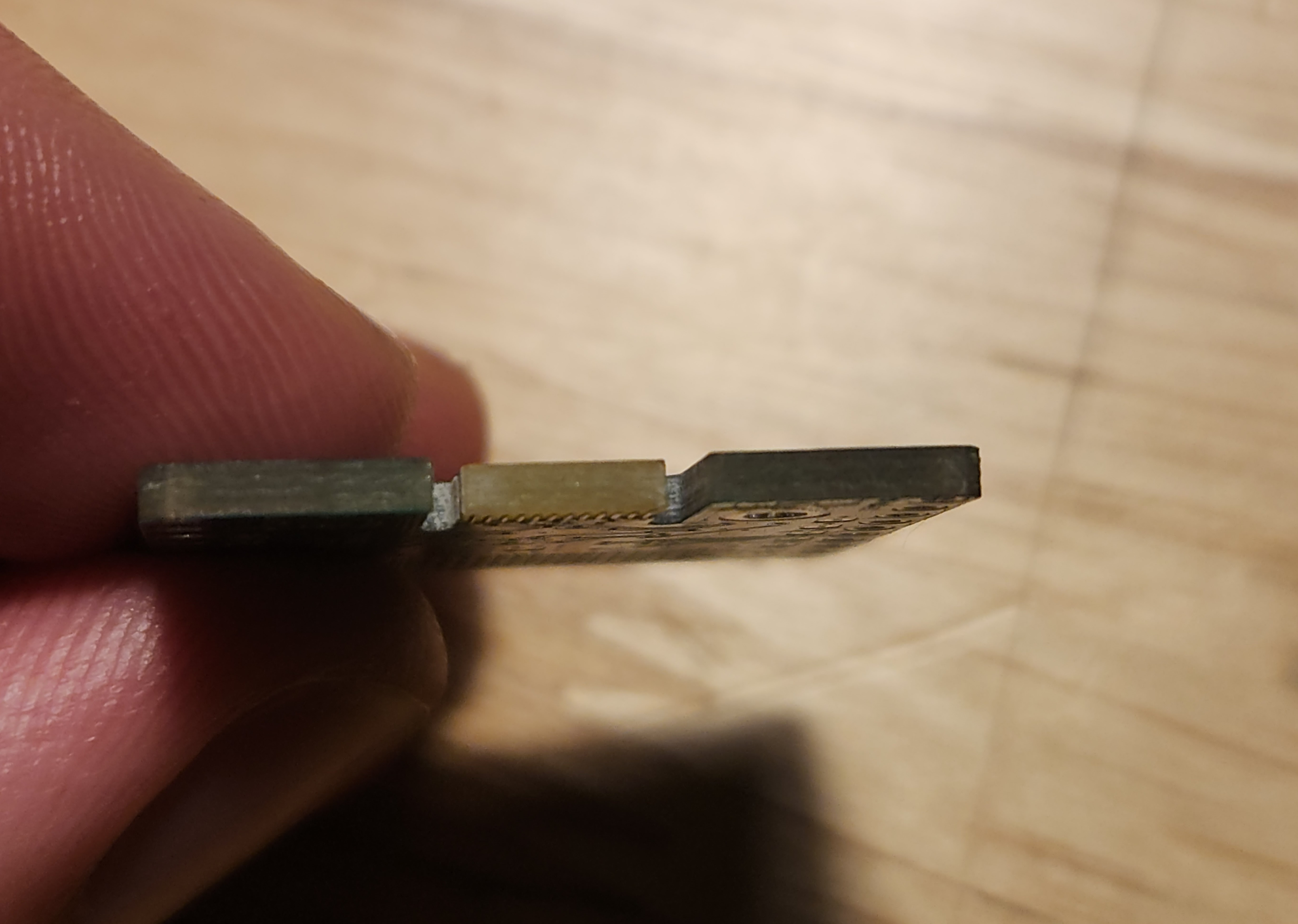

    They Thicc.

    As a reminder, the PCBs need to be around 0.7 mm for this crappy USB-C connector idea to work. The closest option available was 0.6 mm from JLCPCB so it wasn't even a given that these boards would work. Unfortunately, we would not get to see if that 0.1 mm really made a difference because the PCBs that were sent were 1.6 mm! 

    It's pretty easy to tell that is way thicker than we wanted but just to really send the point home here is a comparison...

    Read more »

  • Rev. 1

    Chris08/05/2023 at 04:06 0 comments

    This is going to be somewhat of a retrospective. Over the past year I have been working full time and have been concurrently completing my graduate degree as a full time student . It's been a lot of work so if things get a bit disjointed in the narrative that may have something to do with it. I've got like, two brain cells, so this has not been an easy project!

    The intro may not have made it clear but this was supposed to be a weekend project for a quick, all purpose, dev board of my own. I was shooting for a half step above breakout board for the RP2040. With that in mind a primary goal was to break out ALL the pins. On the stock Raspberry Pi Pico you only get access to 26/30 GPIO pins. I'm paying for 30 pins of GPIO so gosh darn it I want to use all 30 pins if I feel like it! That's of joke of course, I'd be sick of layout too after spending who knows how long laying out custom silicon.

    But then my cheap brain cell gets all worked up with this lofty pin-breakout-goal presented by the flexible brain cell. Why? Because more signals means more pins, which means more board area, which means more money!  So the first question was: how small can I make the make the board. The second question was: how could I break out all the signals in a reasonable way? 

    The answer to the first question was clear: I'd make it 1 square inch. Why? Well that's the size of the RP2040 Stamp, which I'd argue isn't really a development board and more of a daughter board or maybe an SoC. Sure it's technically hand solderable but what's the point if you need a carrier board to even use it? Then it's no longer 1x1 inch! 

    Answering the second question was a bit more difficult. After many minutes of thinking my two brain cells presented me with:

    The Thad - A Through-Hole Pad. 

    Clever name, I know. Hopefully a clever solution too. It's literally just a square pad with sort of small plated through hole down the middle

    Yep! That's all it is! But sometimes the simplest solutions are the best solutions. Obviously this gives you a nice place to solder jumpers, but more importantly, it also allows you to hand solder the board down another circuit board without having to deal with the 2mm pitch of the RP2040 Stamp. The hope is that if everything is tinned properly then the solder will follow the heat down the plated hole and be drawn onto the bottom pad through capillary action. I don't really know what capillary action is but it sounds applicable in this case. 

    Through Hole Pads = Thads!
    Through Hole Pads = Thads!

    Space those bad boys out on a 0.1 inch grid and stagger them with the regular header pins and it feels like just maybe we found a cool solution. There's one more cute little trick that I'll show in the next post that really takes this concept to the next level, so stay tuned. 

    Alright great! So we have the Thads taking care of breakout duty but man, my cheap brain cell wasn't quite satisfied. I mean sure, those pads don't technically cost money, but look at all the space they are taking up! We're only working with one square inch here, buddy! We better do some serious space saving somewhere else. And oh boy did we save some space in promote the most questionable way possible. Presenting: 

    Free USB-C Connector - USB-C, but SKINNY

     If you think about it. What do you really need in a USB-C port? Obviously you'll need the metal contacts because electrons tend to flow better through metal. Or so I'm told. You'll also need something for the metal to sit on, so substrate material is pretty non-negotiable too. The rest? Well, do you really need it? "Strain relief something something," I hear you mumble; but do you really need it. You may say yes, but I say no!

    Hear me out. For something like a phone or a laptop, of course this would be a horrible idea. You would snap this little piece of fiberglass off in an instant as soon as you forget your phone is plugged and try to roll over...

    Read more »

View all 10 project logs

Enjoy this project?

Share

Discussions

neil wrote 02/02/2024 at 12:49 point

Interesting USB-C connector!  Whats the BGA footprint on the rear for? I'm intrigued as the GPIO pins are consecutive - is this for PIO?

  Are you sure? yes | no

Chris wrote 03/29/2024 at 23:04 point

The idea for USB-C connector is what started this whole thing! I pleased with how functional it is. 

The BGA footprint looking thing on the back is actually an SMD prototyping area. It's a great size for an SOIC-8 part. 

The GPIO pins are consecutive because I always get frustrated hunting for pins that might not even be broken on tiny dev boards. The PIO convenience is a bonus!! 

  Are you sure? yes | no

GatCode wrote 08/17/2023 at 06:01 point

Great project! Is there any chance that you can share the source files? I really wanna get my hands on this project - this is such a great idea.

  Are you sure? yes | no

James Newton wrote 08/10/2023 at 04:08 point

Wow. If I could purchase a couple for $20 I would. e.g. "Shut up and take my money!" Any chance of a PCBA run?

  Are you sure? yes | no

Chris wrote 08/10/2023 at 19:53 point

There's a 100% chance! The next revision of the board should be ready for public consumption. Thankfully its just minor bug fixes this time...

  Are you sure? yes | no

Similar Projects

Does this project spark your interest?

Become a member to follow this project and never miss any updates