Close
0%
0%

Dynamic Electronic Load

Yet another DIY electronic load project.

Similar projects worth following
An attempt to make a useable electronic load with 4 modes of operation: Constant Current (CC), constant resistance (CR), constant power (CP), and constant voltage (CV). Up to 400W of load capacity -- either 100V @ 4A, or 40V @ 10A -- but heatsink/fan will determine how much continuous power it can dissipate (hoping for 150W). It will have remote voltage sensing, an OLED display and (hopefully) improved accuracy. It might also have a battery discharge capacity mode.

There has been a lot of DIY effort to make a good, cheap constant current electronic load. I must give homage to the efforts of past attempts, mostly successful, to create something useful for evaluating a power supply's capability or a battery's capacity. It's not easy.

One of the best is Dominik's: https://github.com/Dominik-Workshop/Electronic_load/tree/master

His implementation covers most of the bases and we used it as a benchmark. But it is a bit lacking in user stupidity protection. (And we wanted more.)

Another implementer worth mentioning (besides our eminent Hackaday colleagues) is John Sculley with his excellent treatise on YouTube: https://www.youtube.com/playlist?list=PLUMG8JNssPPzbr4LydbTcBrhoPlemu5Dt

But alas, Mr. Sculley descends into the mire of fixing unforeseen predicaments in a seemingly never-ending fix-it scenario. I guess a nice way of putting it is "Feature Creep".

We recommend viewing Kerry Wong's excellent YouTube videos (https://www.youtube.com/watch?v=WUPrj03UbTM) on Linear MOSFETs for an education in the reality of "Safe Area of Operation", or SOA, for the uninitiated.

A Bit of History

Paul has been working on this for a while. I entered the scene when he had a problem with oscillation that he couldn't explain while evaluating his latest prototype. Paul's blog on this subject is here: https://www.paulvdiyblogs.net/2024/04/

Project Status (2024-06-09):

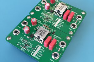
Paul received the latest PCB version (v5.1) a couple of weeks ago. The only significant problem identified so far is that the two fans cannot share a single TACH output.

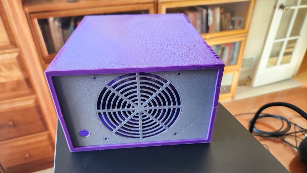
There are now two fans for thermal management. The two fans are wired in parallel -- there are two 4-pin fan connectors on the PCB. One fan, 92mm, sits below the heat sink and blows cool air up into the fins. The other 92mm fan is mounted at the rear of the enclosure and suck hot air out of the enclosure. This has been tested to 180W, the limit of Paul's power supplies. 

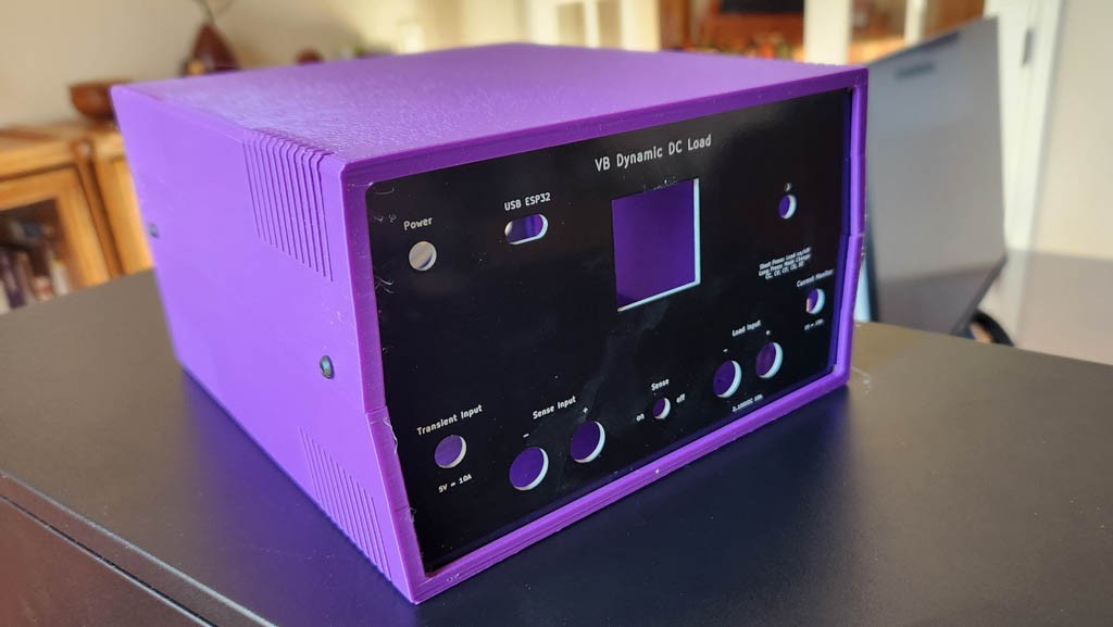
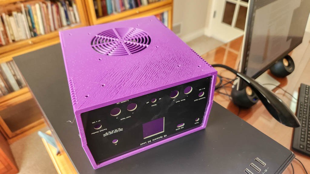
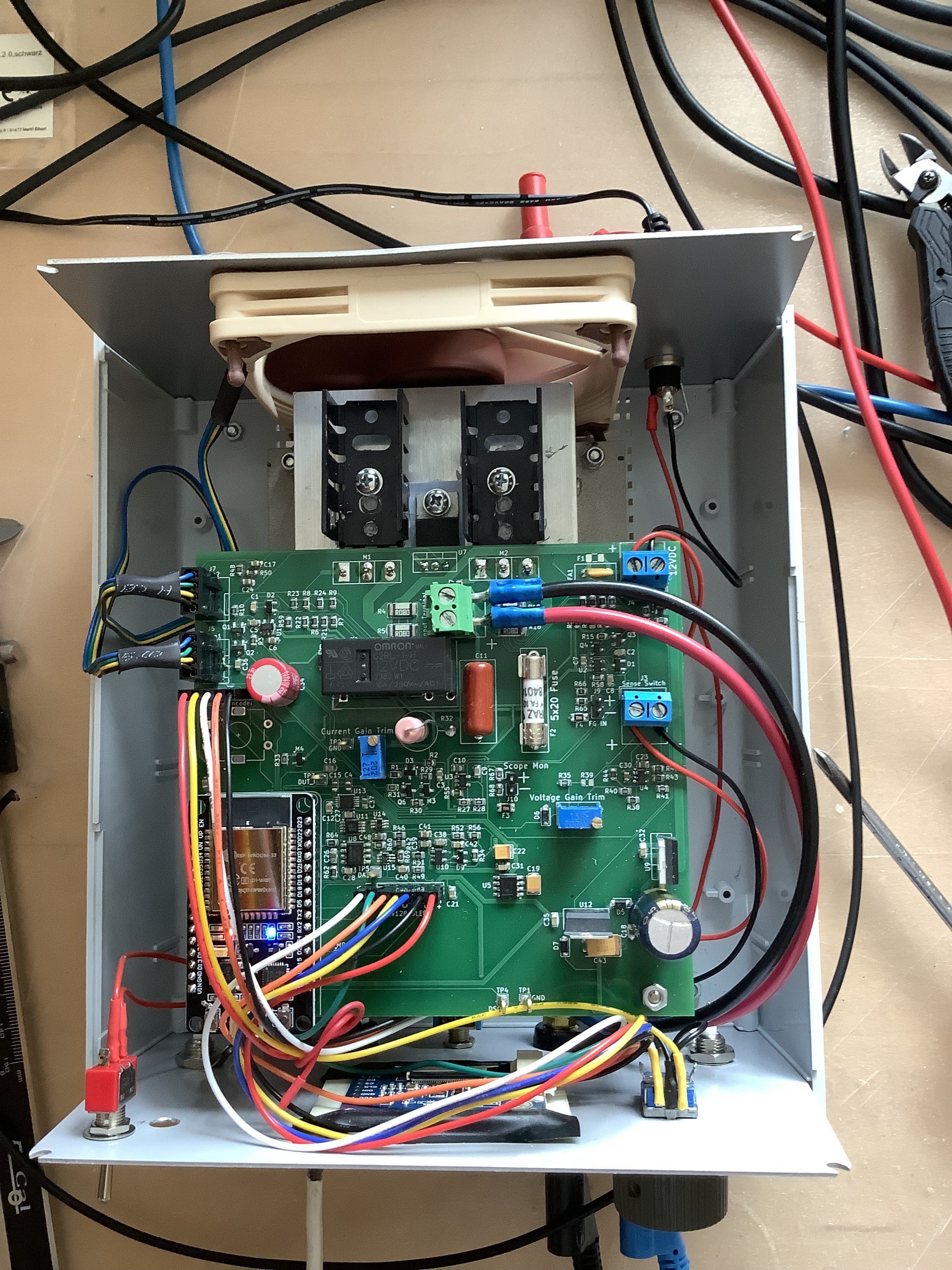
The enclosure is another problem. It should be plastic, to isolate the heatsink (which is connected to the output terminal) from the user. Paul found an acceptable enclosure -- a Teko AUS 33.5 (198x178x108mm) -- but it is not readily available in the USA and the shipping is costly. Paul is going to create PCB panels for the front and back to make it look less DIY, so this is the only enclosure we recommend now. This is what the inside of the enclosure looks like with the current PCB revision:
Target Specs:

Input Voltage: 1V - 100VDC

Input Current: 1mA - 4A for 40V < Vin < 100V, 1mA - 10A for 1V < Vin < 40V.

Maximum Power Dissipation: 150-200W (Depends upon heatsink and Fan.)

Voltage Accuracy: 0.2% (Trimmed, but there are temperature drift terms.)

Current Accuracy: 0.6% (Trimmed. Best guess right now. Mostly temp drift error.)

Lowest Conductance: TBD. (Current NFETs + Sense R + Relay contact R = 75mR)

Ripple: TBD

Protection: Reverse polarity to -100V. 15A fast blow fuse at input.

Power Input: 12VDC/1A Wall Adapter. Reverse polarity protected to -24V.

Cost: $TBD (Maybe $100 depending upon enclosure/fans/heatsink and where you order components.)

User Interface:

Display: 128x128 Color OLED.

User Input: Rotary Encoder with push switch. Remote/Local voltage sensing switch on front panel.

The Software:

Paul is working on it. He's using an off-the-shelf ESP32 DEVKIT.

The Hardware

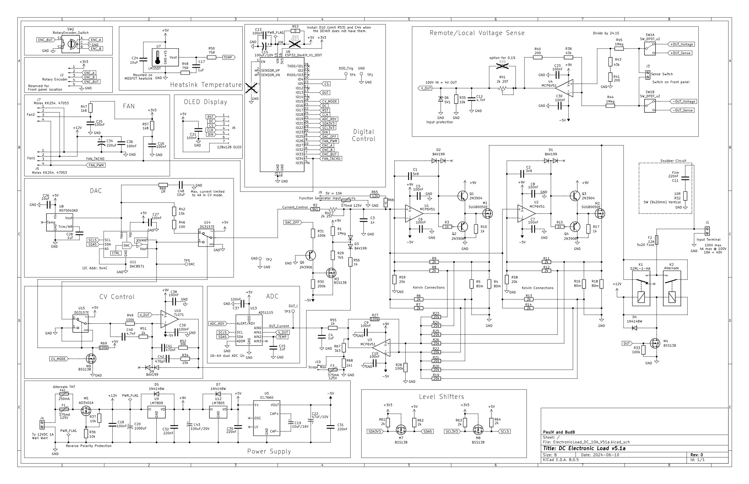
Here is our current working schematic (as of 2024-05-19). Yes, it's all on one page. It's easy to see where all of the global nets go and there's no hunting through interminable itty-bitty letter-sized sheets to find the ultimate termination of a signal path. Sorry to disappoint.

The first thing to notice is that there is a relay and fuse to protect the circuit guts against inadvertent stupidity. It's better to replace a fuse than toss an entire circuit in the trash. The nice things about relays are that they don't leak current when they're open and have decent contact resistance...

Read more »

  • A fork in the road. Getting to 150W

    Bud Bennett05/13/2024 at 23:42 0 comments

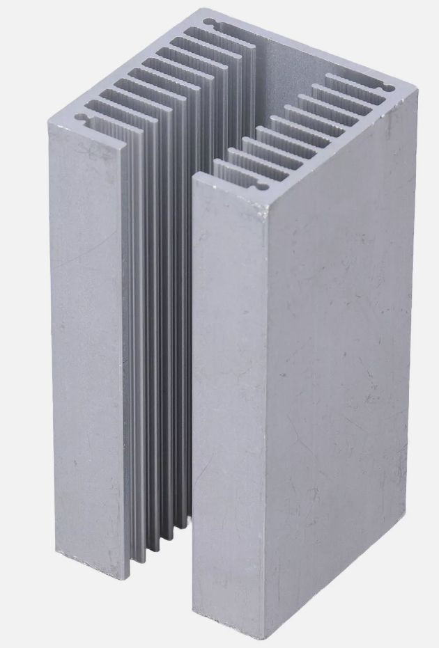
    Paul has a unique heat sink that he is using to shoehorn the board + heat sink into the proposed enclosure. We can't find this particular heat sink anywhere...and if we can't find one neither can you. So I proposed we shift to a "C" or "U" shaped heat sink like this:

    This form has a lot going for it. NFETs can be mounted on opposing sides to more efficiently spread the heat. A small 50x50 fan can be mounted at one end, and the open part of the "C" can be covered with metallic tape to help direct the airflow across the cooling fins.

    This heat sink is not particularly expensive -- less than $15 from an eBay vendor. We see this type of heat sink employed in quite a few commercial EL offerings (and also in Dominik's project.) A 50x50 12V fan is not expensive (Amazon) and can generate more than 10CFM of airflow across the fins.

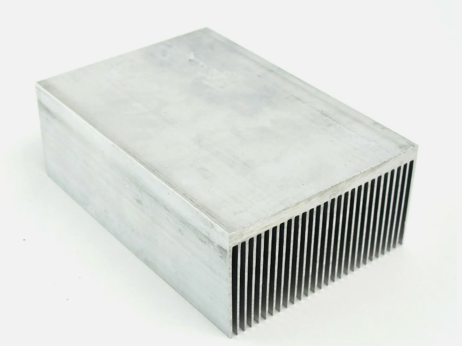
    There is an alternative that we are exploring simultaneously -- a flat finned heat sink that is also widely available, but more difficult to provide directed air flow for cooling.

    We could bend the NFET leads at 90 degrees and mount them onto the top of this heat sink, but directing the air flow is more complicated. My vote is for the "U" shaped heat sink.

    Either of these heat sinks will require a complete redesign of the PCB layout. Ugh.

    Paul has ordered both versions. It will be several weeks to receive the new heat sinks and evaluate their effectiveness. Everything is on hold until then.

  • CV Mode by Hardware

    Bud Bennett04/11/2024 at 14:54 0 comments

    Paul and Bud originally thought that the Constant Voltage (CV) mode would be implemented in software, like the Constant Resistance (CR) and Constant Power (CP)  modes. Bud kludged together a possible HW CV implementation and it worked in principle, but was not optimized and considered "optional" on the schematic. Paul gave up on a software implementation a couple of days ago.

    Apparently CV mode is difficult to accomplish in software. Keysight implements it as a hardware loop in their 6060B and 6063 electronic loads. If you want a head-splitting headache take a look at the schematic in the Keysight service manual for those instruments. Some cheaper bareboard electronic loads implement it poorly. And some commercial electronic loads, such as the Array 371, don't implement CV at all.

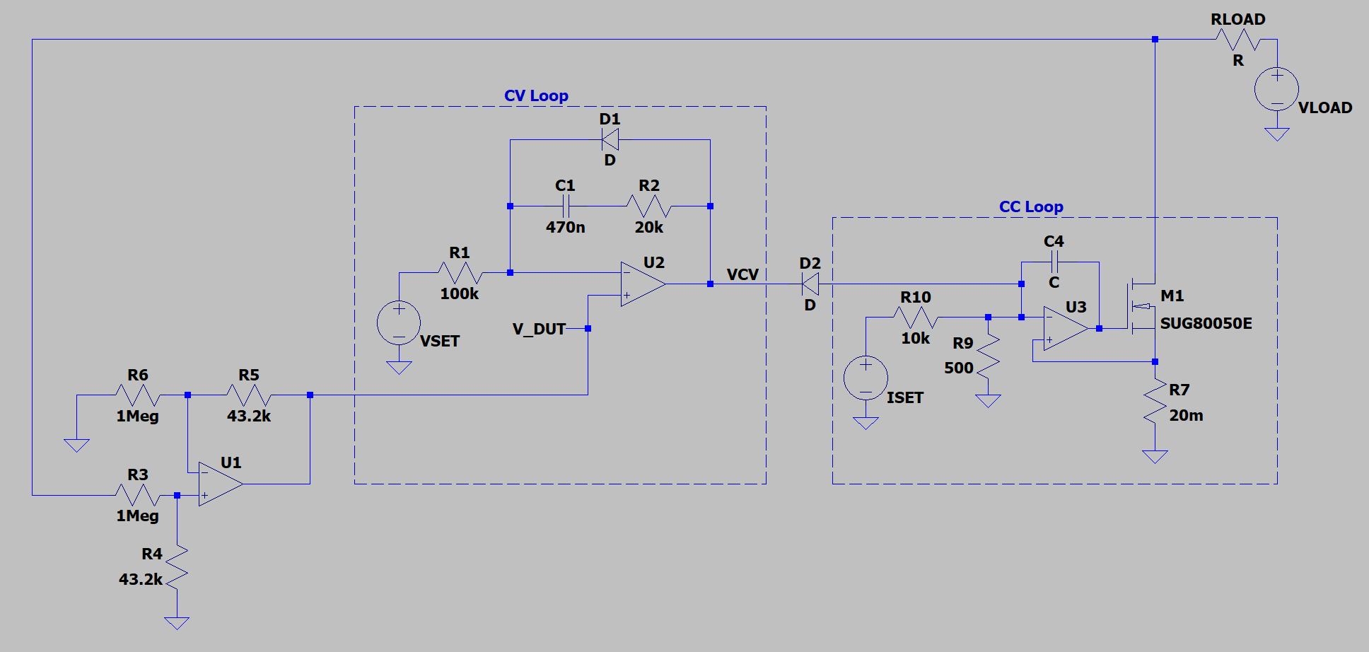
    Our implementation is a bit simplistic as shown by the simplified circuit below (don't get too hung up on component values):

    In normal CC operation, VSET=0V and the VCV node is clamped at least a diode drop above GND. This effectively removes the CV loop from interfering with the CC loop since the highest voltage the divided ISET voltage can provide to the input of U3 is 200mV. 

    In CV operation VSET is a voltage between zero and 4V, which equates to a load voltage of 0-100V. ISET sets a maximum output current for the current loop and the CV loop decreases that current, by forward biasing D2, until the current at the load balances. This will happen when V_DUT equals VSET. There must be a current limited voltage source or a series resistor, RLOAD, in place for this to work. The astute observer will note that the voltage feedback is via the "+" input of U2 and therefore there is nothing controlling the CV loop dynamics except what is available in the CC loop. The easy way to see this is realize that at high frequencies U2 is essentially a voltage follower to its + input. This may prove to be a big mistake. It would have been preferable to use two inverting opamps in the CV loop so that the V_DUT signal would be attached to the "-" opamp input and separate loop dynamics could be implemented. (Like what Keysight did.)

    The baby is ugly, but can it perform the function?

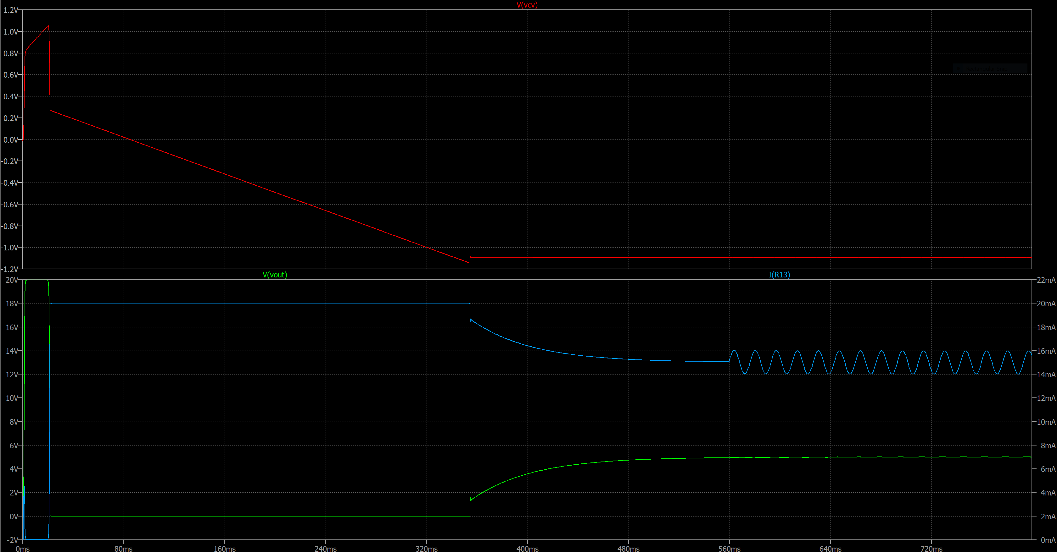
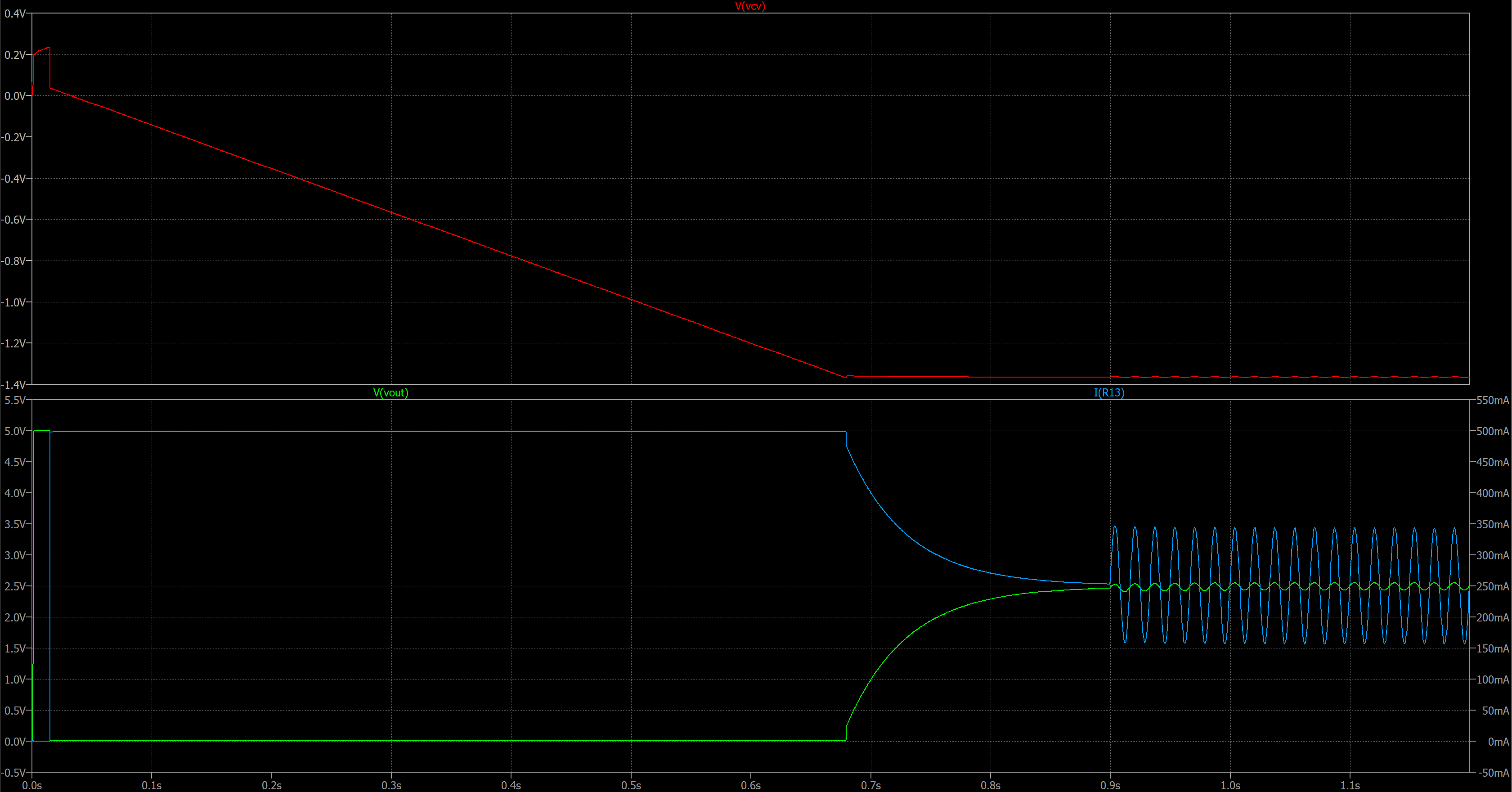
    It appears so, but as of right now we only have simulation to rely upon (and simulation is not reality). Here's a simulation result showing the system at startup. The parameters were VLOAD=20V, RLOAD=1k, ISET = 0.05 (125mA max) and VSET=0.2V (5V). The green line is the load voltage. The red line is VCV and the blue line is the load current.

    The system is held at zero output current for 5ms and then released. The CV opamp is out of control until VSET changes from zero to 0.2V, but it has to slew to 1.2V below GND before it takes control from the CC loop. Since the CC loop can output 125mA it drives the output voltage to zero (125mA x 1k = 125V, but only 20V is applied). Once the CV loop overcomes the CC loop the current decreases in the CC loop and the load voltage rises to the set point (5V). A 1V-peak sinusoid on top of VLOAD is applied at 560ms to show that the CV loop can keep the output voltage stable when disturbed. I think it performs pretty well, if slowly.
    But slowly might be OK. The way that Paul is approaching the user input is to start at low values and have the user scroll the setpoints to whatever he/she desires. A user is a pretty slow animal too.

    To demonstrate the other end of the spectrum, here is a different set of conditions/parameters: 

    The input voltage is only 5V and the max CC current is set to 10A. RLOAD = 10R and VSET = 0.1V (2.5V). Note that the CV opamp takes longer to slew to start controlling the CC loop, but the result is pretty much the same. There is a lot more disturbance caused by the 2Vp-p wiggle on the load voltage, which begins at 900ms. Still, the reduction in load voltage wiggle is substantial.

    At this point in the design process Bud is hoping that the CV mode is "good enough".

  • Forcing Zero Current

    Bud Bennett04/04/2024 at 21:25 0 comments

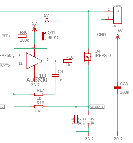
    When the system boots up the relay should be open and the CC DAC should be set to zero. But this doesn't necessarily set the output current to zero. If the opamps controlling the current loops have a positive offset they will be unable to fix the current at zero. And if the offset is negative the opamp output output will drift to its negative supply if not constrained. Therefore, the only way to get zero current is to force it through some other means.

    Dominik solved this problem by yanking the opamp input to a high voltage, which drive the output to its negative supply. This does enforce a zero current state at the output, but not without issues during normal operation.

    The leakage current from the collector of Q11 is not usually a term anybody cares about. In this case, the S9015 has ICBO=50nA, which is pretty low. This current generates an offset term across R18 equal to 0.5mV, or 5mA per opamp (and there are 4 of these, but not all will generate WC leakage current). In our case, it would create an output current error equal to 12.5mA.

    The Keysight design just yanks downward on the opamp output, forcing the opamp to output short circuit current. This is bad because the opamp generates a relatively large output current, but is good because any error current from the downward yanking device gets swallowed by the opamp in normal operation and doesn't impact performance.

    Both of the approaches above force the opamp into a state of inequality. The output is driven to a rail and the inputs aren't equal. When the opamp is released from this condition there is usually a transient spike of uncontrolled magnitude until the conditions of equilibrium are re-established. Generally not good.

    Our Approach

    We chose a different path. 

    The BAV199 low leakage diodes are actually specified over temperature and voltage! They're spec'd at a max reverse leakage of 5nA at 25C, and 80nA at 150C. The datasheet even provides data for typical and max leakage current as a function of temperature: 3pA typical at 25C, 300pA typical at 100C, 5nA max at 25C and 30nA max at 100C. 

    In normal operation D3 leaks current into the "+" input of the two opamps controlling the current loops, getting absorbed by the 500R equivalent resistor at that input. But this is partially compensated by a reversed biased D2 leaking current into the "-" input of opamp U1 (and D1 leaking into U2), getting absorbed by the 1k resistance at those inputs. The currents are not going to match, so we can use typical vs worst case to see what the range of error might be. But the difference between typical and WC is so large that the typical value can be set to zero. If D2 is leaking worst case then it will produce an output current error equal to -(30nA x 1k)/0.04R = -750uA. If D3 is the WC condition then it will produce an error current equal to +(30nA x 500)/.02R = +750uA. So it seems the error current will drift somewhere between +750uA and -750uA WC as the box heats from 25C to 100C. If we use just typical numbers then the offset error drift is only -7.5uA. That's manageable.

    How it works

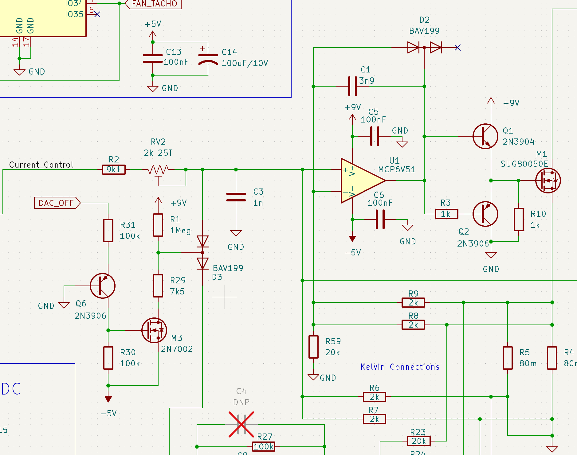
    Normally, the DAC_OFF signal is low (zero volts). Therefore Q6 and M3 are "off" and the BAV199 diode, D3, is reversed biased and not influencing the current loop significantly. If the DAC_OFF signal is asserted to 5V then Q6 drives the gate of M3 to a VGS ~ 4V and M3  switches "ON", which then pulls its drain to -5V. R29 then forward biases the upper diode of D3 and pulls the "+" input of U1 below ground. The amount of negative voltage at the "+" input of U1 depends upon what the DAC value is. If we assume the DAC is outputting 4.096V or less, then the opamp "+" input is yanked below GND. Since the gate of M1 can't go below GND the opamp output will drop, forward biasing D2 until the opamp inputs equalize...somewhere around -1V. R3 is there to limit the current into the base of Q2. So now the gate of M1 is at GND and there is just leakage current flowing through...

    Read more »

  • PCB Layout Effects on Performance

    Bud Bennett04/03/2024 at 20:50 0 comments

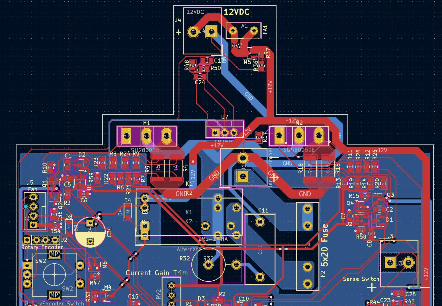
    As of this date (2024-04-04) the PCB layout is frozen for this pass. I've been fiddling with it for several days -- making small changes that never seem to end. Here is the layout of the high current/high voltage section:


    At the last minute we're specifying 1oz copper for this PCB. That change increased the traces carrying 10A blow up to 6mm width and the traces carrying 5A are now 2.5mm wide.

    The GND reference

    The first thing to notice is pin 2 of J1 (find it just below and to the right of U7) -- that is ground zero for the entire PCB. It is the absolute GND reference potential for the system. This is where the negative input lead of the load connects to the PCB. All of the various power inputs and outputs connect to this point. The 12VDC power adapter negative lead (in Blue) snakes around to the right and comes directly to that lead (a Kelvin connection). The top-side metal traces (in Red) that bring currents from the sense resistors, R4-R5 and R8-R16, are split equally/identically in terms of resistance, from those resistor's pads to J1 pin2. Those traces carry a maximum of 5A/each and are properly sized, by width (2.5mm), to carry that current without over heating.

    The snubber capacitor, C11, also connects directly to the J1 pin2, but with a much smaller trace width since the currents should be smaller.

    Lastly, the ground plane is almost a Kelvin connection but must share a small section of bottom-side metal trace. Hopefully, it will not matter much.

    High Current Paths

    The high current traces carry 10A max and require a trace width of 6mm. The input connector, J1, has a 6mm wide trace (in back-side metal, Blue) from it's positive terminal to the fuse, and also from the fuse to the relay (back-side metal, Blue), where the trace eventually splits and reduces to 2.5mm to handle the 5A currents to the drains of M1 and M2. 

    High Voltage and Creepage

    The pads of the high voltage devices/connectors must have sufficient distance from other pads to prevent creepage. High potential between pads located close together can develop conductive "growths" that cause parasitic currents to flow and can eventually cause failure. This is not only a problem for exposed pads or traces that are not covered by the solder mask. The recommended pad separation distance to prevent creepage for a 100V potential is about 1.5mm. Traces located under a solder mask only need to be separated by 0.4mm to withstand 100VDC. The layout conforms to these restrictions.

    Kelvin Connections

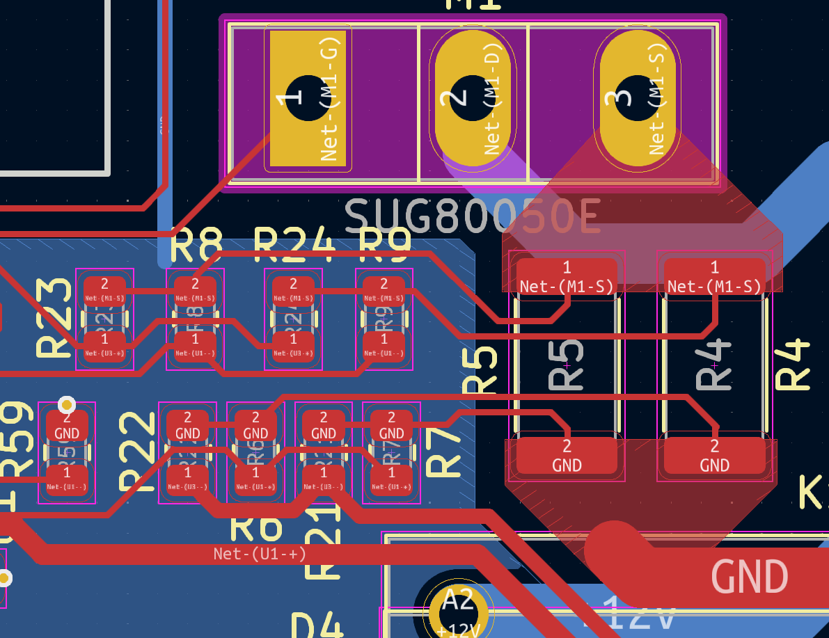
    I'm assuming this technique is named after Lord Kelvin. Here is the layout detail on the left side:


    The current tends to spread in 45 degree funnels from a single point to a connection point, such as a pad on a component. In order to make the Kelvin connection the current should be zero at the point of the Kelvin connection. I made triangular copper pours to distribute the current to the two sense resistors. The back-side of the pads should have zero current flowing to it and therefore a good place for a Kelvin pickup. The pickup points are on the middle-inside of the pads on the sense resistors. Those traces connect the feed resistors for sensing the voltage across the sense resistors.
    There is another method of picking off Kelvin connections from SMD devices, but this method was recommended by the manufacturer of the sense resistor...who am I to argue. We'll see how well this performs when we get the PCBs to evaluate.

  • Accounting for Errors in the CC loop

    Bud Bennett04/01/2024 at 23:48 0 comments

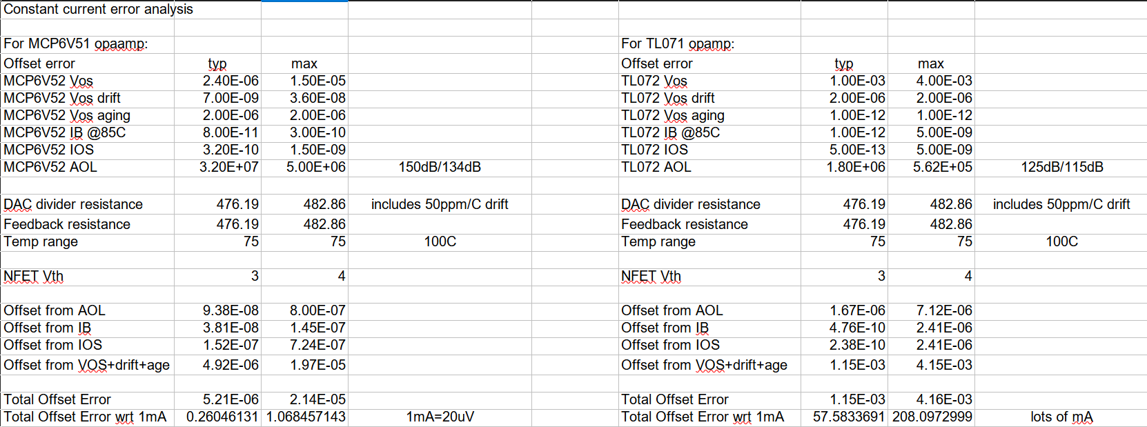
    We have the topology selected that minimizes gain errors to a first order -- primarily resistor tolerances. What opamp will give us the best bang for the buck when it comes to all of the errors associated with the amplifiers? I put together a spreadsheet to add up the various errors caused by the opamp.

    For perspective, it is worthwhile to note that 1mA of current requires only 20uV of voltage across the 20mR sense resistor.


    I have used a MCP6V51 opamp on another project and was impressed. It is a chopper-stabilized (i.e. zero-drift) opamp with incredible specifications. On the right side of the spreadsheet is the TL071 -- a general purpose JFET-input opamp. The first section lists each opamps specs wrt input offset voltage and input bias/offset current, as well as the open-loop gain (AOL) for both typical and worst-case values. Below that I calculated the effective resistances at the inputs to the opamp and the expected maximum temperature range (25-100C).

    AOL Error

    In this application the amplifier has to drive the NFET gate to around 3-4V before any current flows in the NFET. If the open-loop gain is low then the amplifier will require more voltage difference between the + and - inputs, which incurs an error. The MCP6V51 has a typical open-loop gain of 150dB (32 million V/V) vs. the typical TL071 AOL of 125dB ( which isn't shabby at 1.8 million V/V). To output 3V the MCP will need a voltage difference of 94nV vs. 1.7uV for the TL. Under worst-case conditions, the MCP needs a difference of 0.8uV vs. 7.1uV for the TL. So the the lower AOL causes about 0.3mA of error from the TL vs. only 0.04mA of error from the MCP.

    Input Current Errors

    Input bias current and input offset current errors are typically better for the TL but worse for the worst-case specifications.  They are small for both opamps.

    VOS Error

    The input offset error is the biggie, and it's made worse with temperature drift. Worst-case VOS for the MCP is nearly 20uV, which is 1mA of error. Worst case VOS for the TL is more than 4mV -- an error of  more than 200mA. Even the typical TL VOS error is nearly 60mA.

    Temperature Drift

    The initial offset of the system can be removed by measuring and storing the offset current. But as the box heats up from a high wattage load the offset and gain terms will drift, causing errors. If you compare the VOS drift terms between the two opamps there is a clear winner. The MCP has 50X lower drift over temperature.

  • Opamp Topology Analysis

    Bud Bennett03/28/2024 at 23:03 0 comments

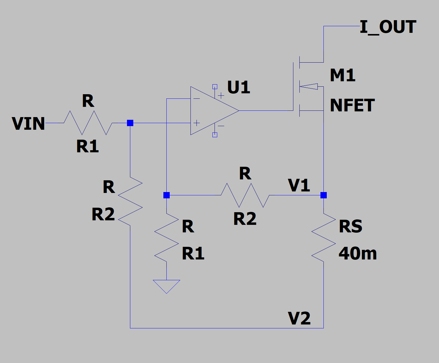
    After we got the Constant Current (CC) loop stable it was time to account for the configuration of the circuit -- the topology. We stumbled upon a topology that appears to yield very good accuracy with the addition of just a few resistors. This is the basic topology of a single current loop:


    What we need to know is how the output current depends upon the input voltage, VIN. The schematic above uses only 2 values R1 and R2 as a special case of this topology that we employ. V+ and V- are the voltages at the inputs of the ideal opamp (infinite gain, no offset). The equations that govern this are:

    V+ = (VIN - V2)(R2/(R1+R2)) + V2

    V- = V1(R1/(R1+R2))

    Since the opamp forces V+ = V-, when you solve for V1 it yields,

    V1 = VIN(R2/R1) + V2 , as you would expect.

    And the output current, I_OUT is therefore:

    I_OUT = (V1 - V2)/RS = VIN(R2/R1)/RS

    Note that V1 and V2 drop out of the equation. Like an instrumentation opamp. The only errors are the ratio of R1/R2 and the value of RS.

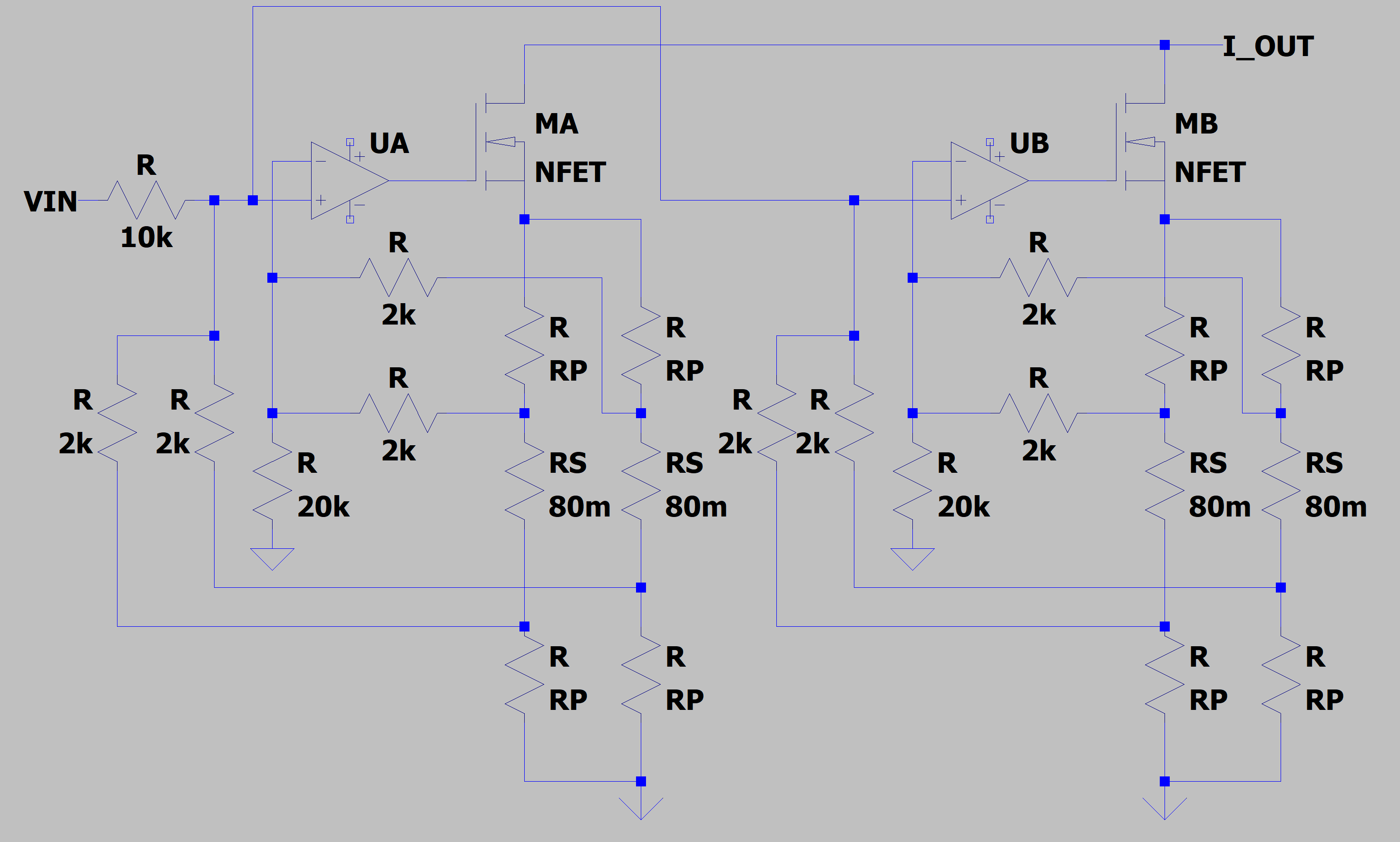
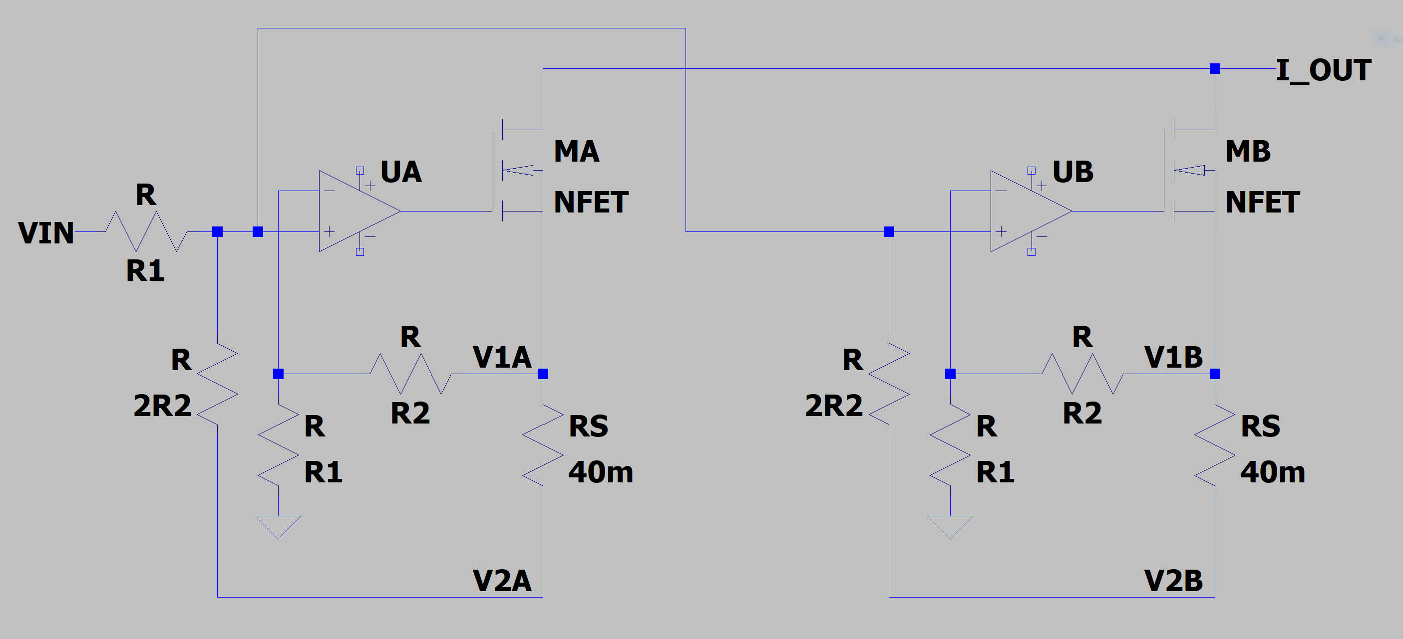
    When we expand the topology to two separate current loops we get this simplified schematic. Again, the resistors values are special cases to match the topology and make the math easier.


    Now it gets a bit more complicated. We want the current, I_OUT, to be only a function of the input voltage, VIN. Here's the equation for V+, which is the same connection for both opamps:

    V+ = VIN R1/(R1+R2) + R1/(2(R1+R2)) (V2A+V2B)

    and since V+ = V-,

    V1A = VIN(R2/R1) + V2A/2 + V2B/2

    But what we really need to know is what the output current is:

    I_OUT = IA + IB = (V1A - V2A)/RS + (V1B - V2B)/RS

    The opamps are forcing V- to equal V+, and therefore V1A = V1B, we can substitute :

    I_OUT = IA + IB = (V1A - V2A)/RS + (V1A - V2B)/RS = 2(R2/R1)VIN/RS, 

    which is only dependent upon VIN and the three fixed resistor values. Of course, this is a trick of a sort since I've forced the resistor values to be identical or 2X multiple. But the errors in the method are below the tolerance of the resistors (sub-1%).

    By inspection, it is obvious that if the "B" side of the circuit has errors that increase the current through MB, then a corresponding decrease in current will occur through MA. In order to prevent this disparity from getting too large careful layout symmetry between the two sides must be preserved.

    *********************************************

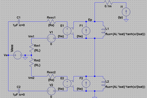
    The next step in the process is to expand the sense resistors to two sets of two. This is to keep the power dissipation in the resistors to a reasonable limit. The math gets a bit unreasonable (for me) and so I resorted to LTSpice to corroborate the result -- it is the same.

    This time I have inserted parasitic resistors, the ones labeled RP, to indicate where the various error voltage will come from. The values of RP depend upon the quality of the PCB layout -- they are not all the same. Note also that the ground return point of the current could be different than the ground reference of Vin. The errors will still be cancelled to a first order. Again, you get the same result, if you keep the resistor values in the same ratios, the output current is only dependent upon VIN, R2/R1 and RS.

    **********************

    The 2kR resistors must be Kelvin connected across the sense resistor, RS, in order to get the full benefit of this approach.

    Simulation Results:

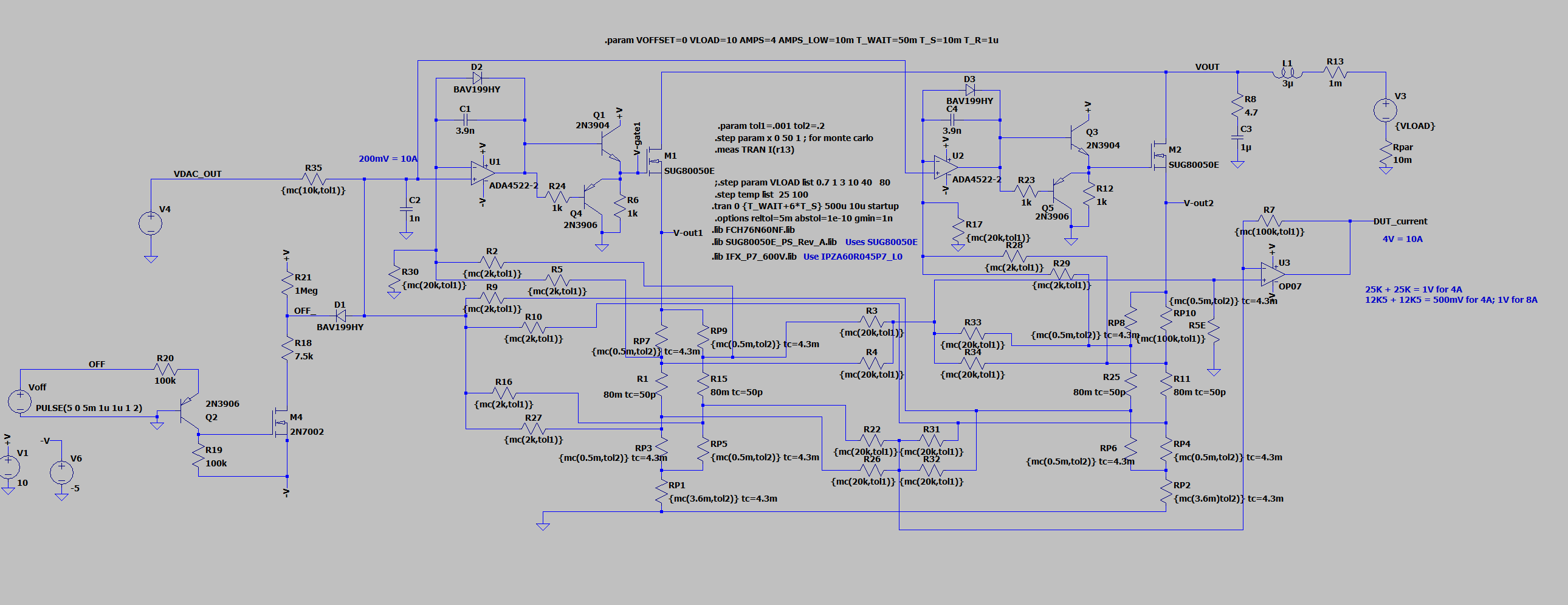
    To prove the point I simulated the circuit in LTSpice using monte carlo analysis. Here's the complete circuit:

    The tolerance of the gain setting resistors is 1%, but I set them to near 0% in the first simulation while letting the parasitic metal trace resistors have a tolerance of 20% and a tempco=4300ppm/C. The siimulation ran 50 times at 25C and 50 times at 100C. The results were uninteresting to say the least -- total variation in output current from the 10A set point was...13.6uA. That doesn't include any opamp variation except temperature. That is a variation of only 0.000136%!

    When I added a 1% tolerance to the...

    Read more »

  • NFET Selection

    Bud Bennett03/28/2024 at 22:52 0 comments

    I had picked out quite a few NFETs that I thought would be good candidates for this project: IRFP150, IRFP250, IRFP350, IRFP460, etc.

    After reviewing Kerry Wong's video about linear FETs I went back through my list of candidate NFETs and culled out most of them. Nearly all of them did not specify a SOA under DC operating conditions...big red flag! I then went back to DIgikey and LCSC to see if there were any that would satisfy our SOA of 100V @2A. 

    I found these: 

     SUG80050E (Still the best one) 

     FCH76N60NF (OK and I have a simulation model)

     IPZA60R045P7 (can't get the sim to run with this spice model) 

     IXTH60N20L2 (expensive and no model) 

     IXFH56N30X3 (ditto) MS170N15IDC0 (Chinese, but specs look OK. Needs derating. No model.) 

     NVHL055N60S5F (no model) 

     RU1Z200Q (Chinese.)

    Without a SPICE model it is difficult to tell if it will work in the circuit. Therefore all I can do is list them as potential substitutions for the one we eventually pick, which right now looks like the SUG80050E.

  • Making a current source that doesn't oscillate

    Bud Bennett03/26/2024 at 00:16 0 comments

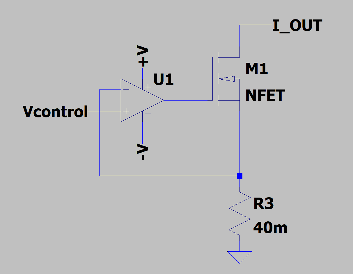
    I've seen some DIY articles that show the most basic topology for making a current source controlled by a voltage source. Here is a typical topology:

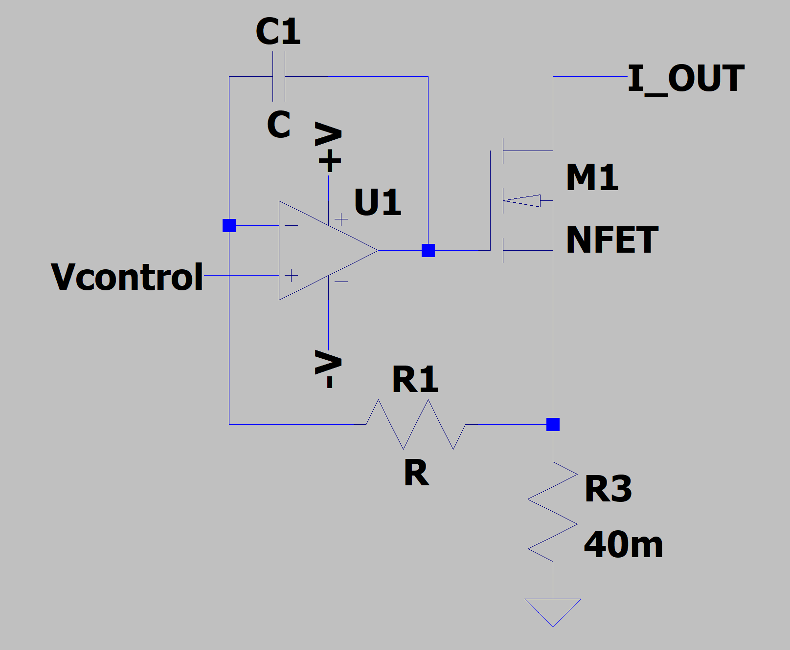
    There is no compensation to prevent oscillation -- it assumes that the amplifier has infinite bandwidth and infinite gain. A more practical circuit might be this one:

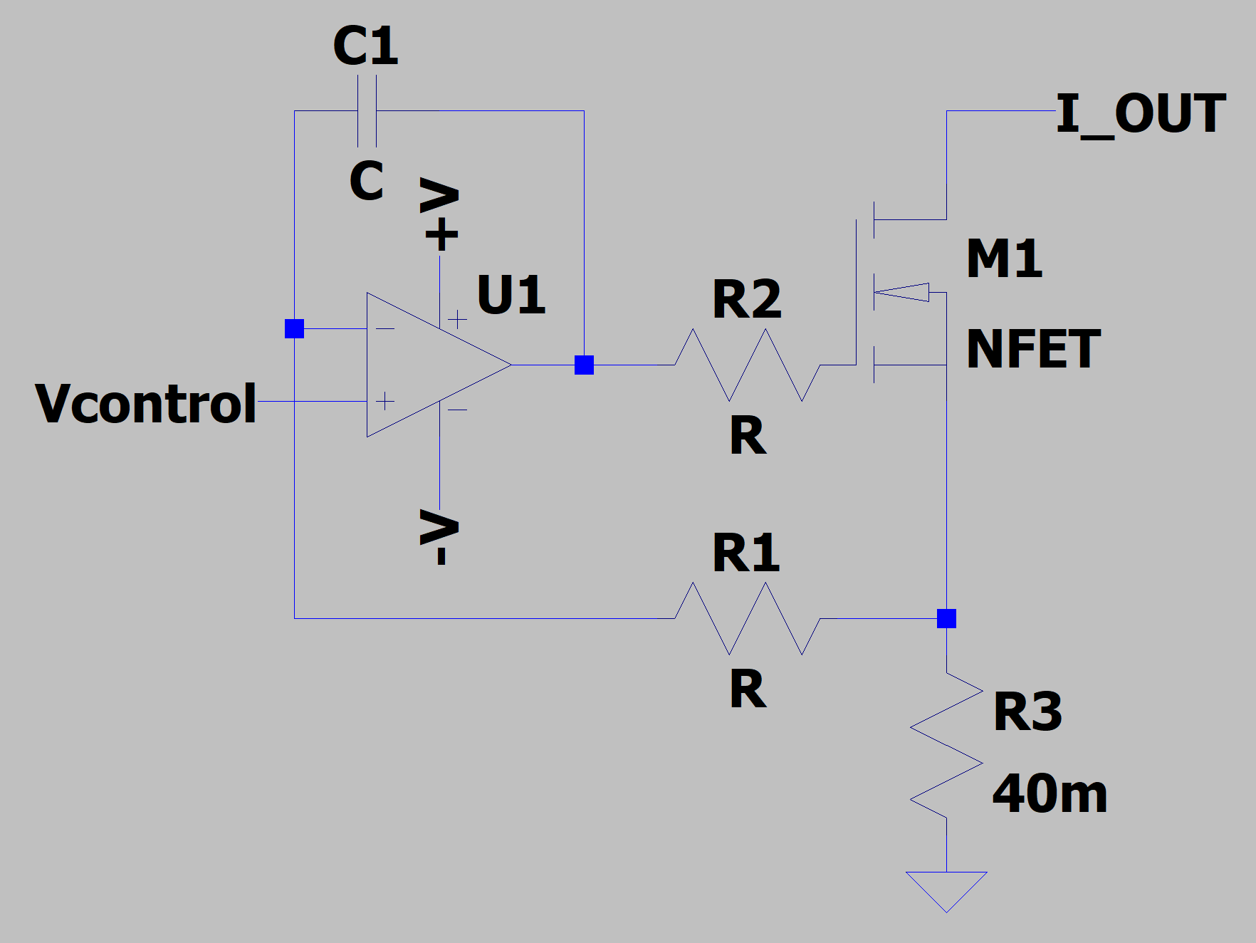
    R1 and C1 create a "pole" that overrides the opamp's internal compensation to possibly prevent the circuit from oscillating. But this still neglects real world problems. Consider the circuit below:

    R2 is added because the gate capacitance of M1 is large (maybe 10nF), which causes the amplifier to become unstable and oscillate. Adding R2 "isolates" the amplifier from the capacitance of M1. R2 is typically 50-300 Ohms. Now we're getting close to something useable.

    Our Approach at Present:

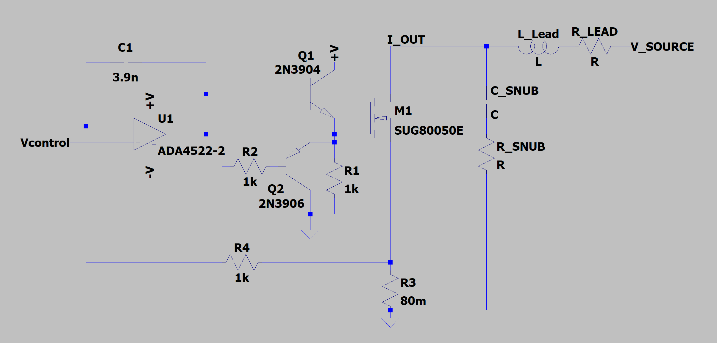
    Oooh...lots more components. This schematic accounts for the inductance of the leads connecting the source to our load. The inductance of the leads makes a big difference in compensating the circuit to prevent oscillation. The values of R_Lead and R_LEAD vary with the length of the wires used to connect V_SOURCE to our load. Typical numbers for L_Lead and R_LEAD are 3uH and 100mR, respectively.

    The addition of Q1 tends to isolate U1 from the gate capacitance of M1 and still provide plenty of current to drive the gate. Q2 doesn't do anything...yet. R4 and C1 create a unity-gain crossover that is low enough that the phase shift through the circuit doesn't reach 180 degrees to cause it to oscillate.

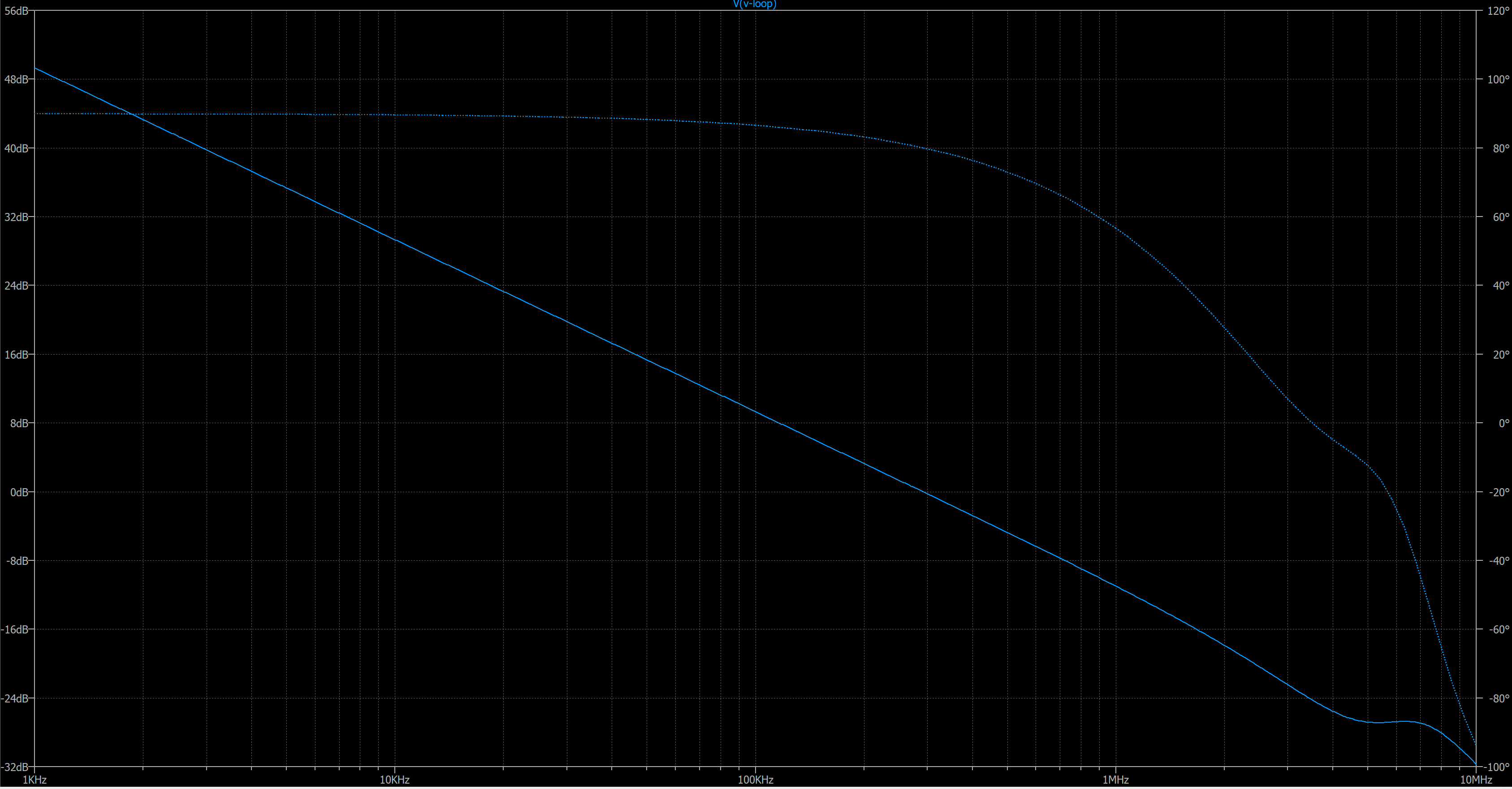
    With R4xC1 having a short time constant (high frequency) the open loop response of the circuit would look something like this:

    Note that the phase margin is nearly 90 degrees and the gain margin is 25 dB, indicating that the circuit is very stable and unlikely to oscillate. But what happens when we include the lead inductance?

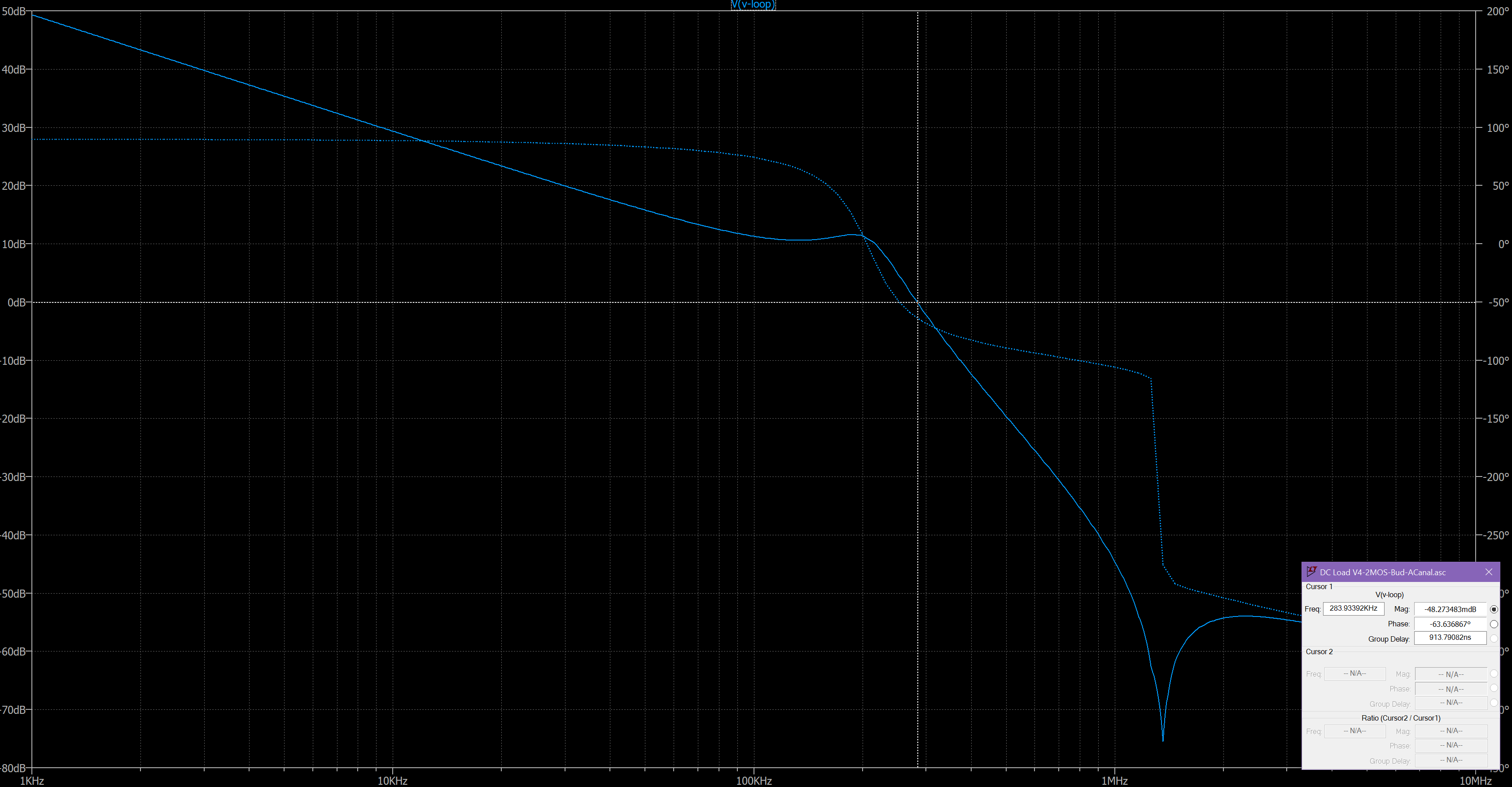
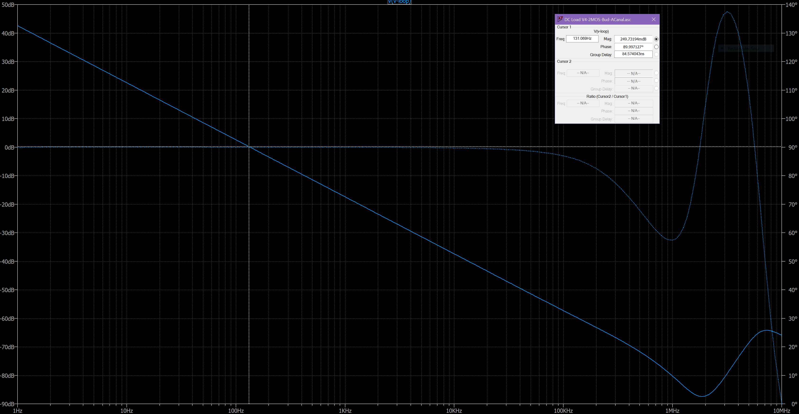
    Now the phase and gain indicate that the circuit will oscillate about 283KHz. It's pretty ugly. It has to be taken into account in the design. The most straightforeward way to compensate for the lead inductance is to de-Q it so it doesn't create a large peak in voltage. That's where the snubber circuit comes in. If we add about 5 Ohms of resistance across the lead inductance it will reduce the Q of the resonant circuit and help prevent that oscillation. Here's what the open-loop response looks like with RSNUB=4.7 and CSNUB=1uF:

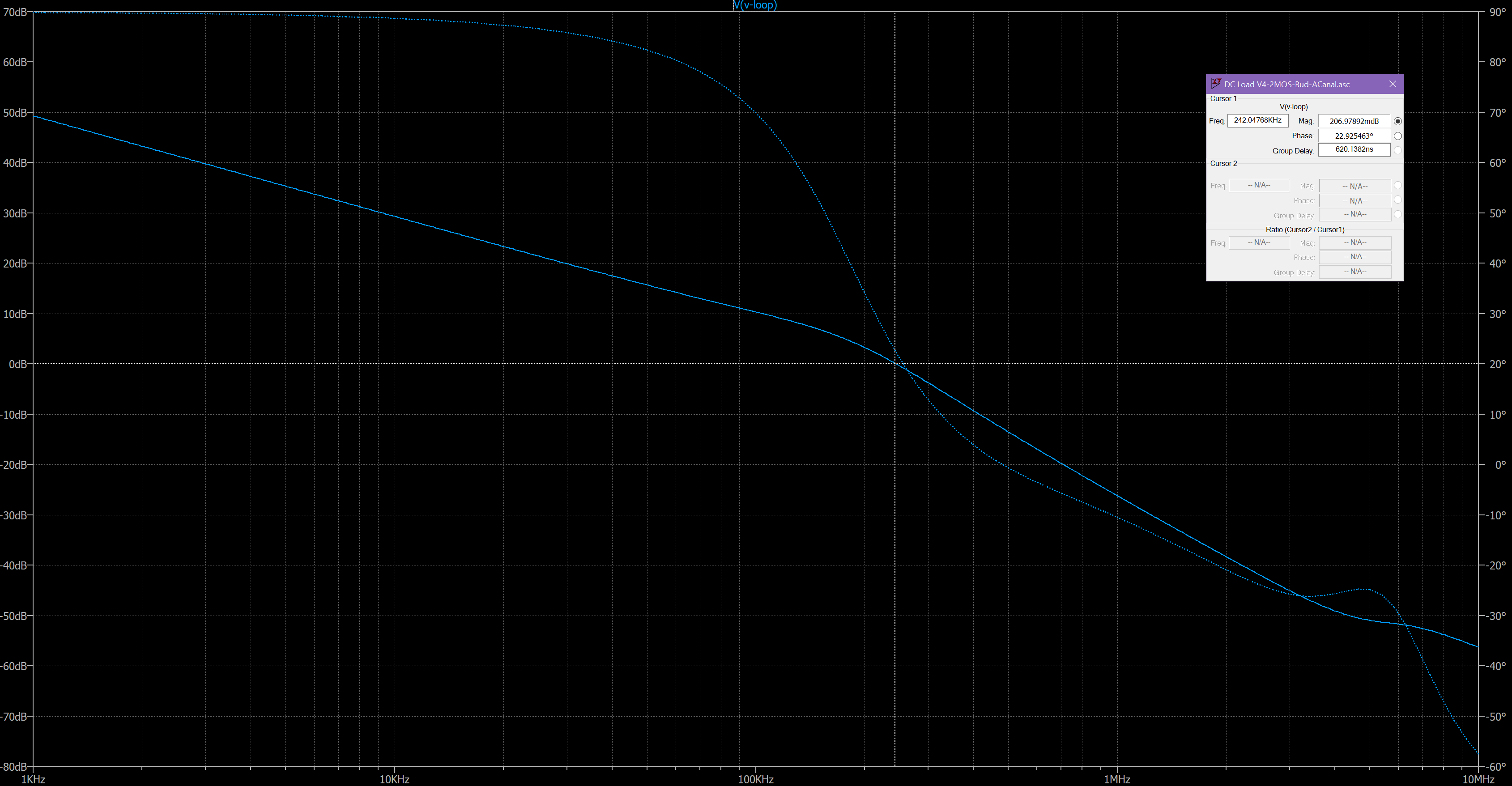
    It's better, but the slope of the gain is too steep and the phase margin is only 23 degrees -- not good enough. Also notice that there is a peaking in the gain/phase response at 5MHz -- stay away from this. The easiest fix to increase the phase margin is to increase C1 until you get adequate phase margin. So increasing C1 from 300pF to 3.9nF gives us this:

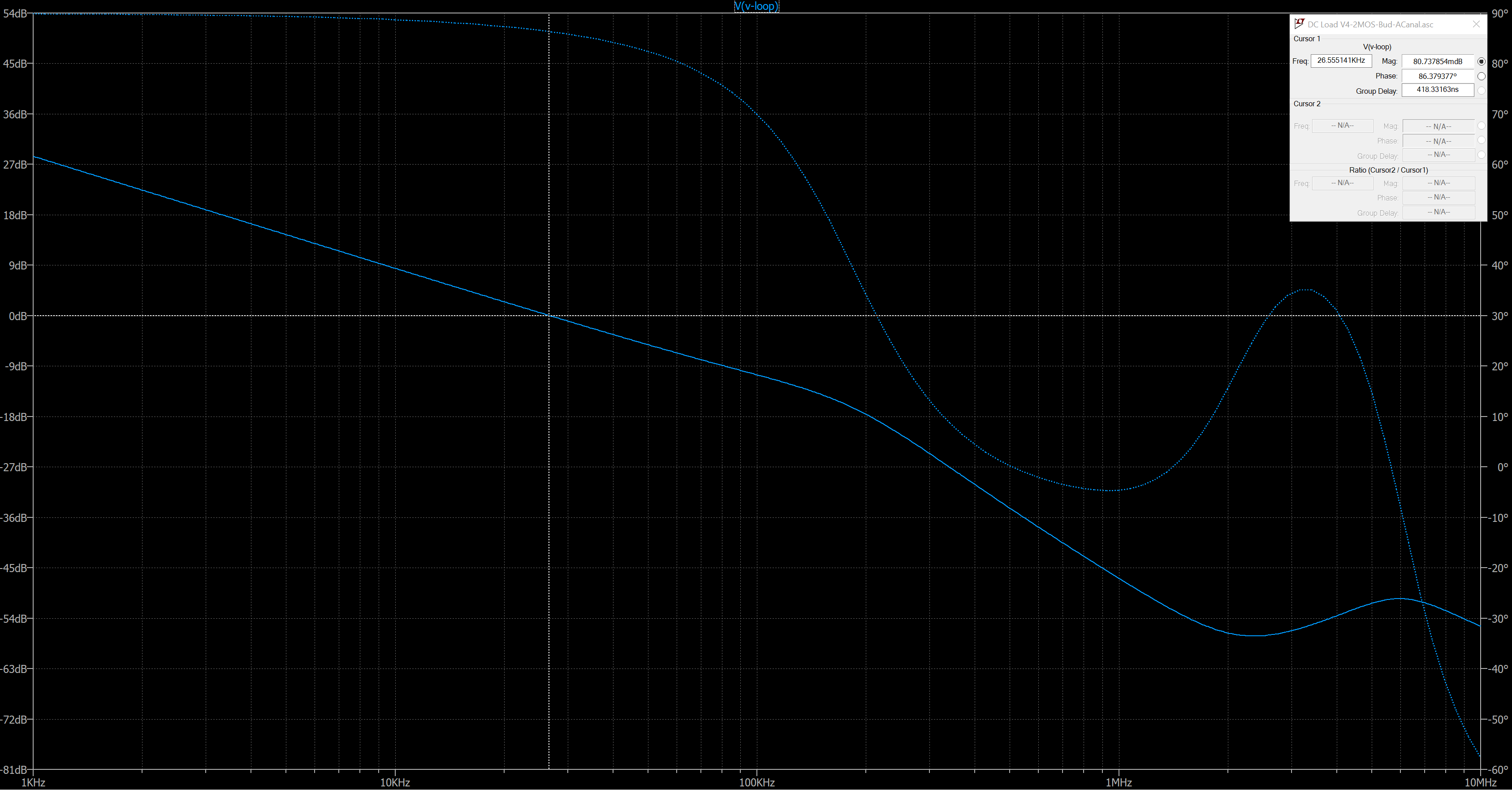
    This looks even more problematic, but it's not. Note that the gain slope as it crosses through zero dB is only 20dB (very desirable for a stable amplifier). Note also that the phase margin has increased to 86 degrees and the gain margin is around 35dB. What we have given up is bandwidth since this loop only has a gain-bandwidth of around 25kHz. But that should be good enough for our purposes. We still need the snubber because without it the phase margin would still be near 90 degrees, but the gain margin degrades drastically to less than 10dB, which is marginal to prevent oscillation.

    But wait...there's more. If we decrease the set point current from a high current to a very low current, say less than 25mA, the gain-bandwidth of the loop decreases to around 130Hz. This smaller than desired, but probably still usable.

    So what are the other components for?

    R1 provides current to decrease the emitter resistance of Q1 and also drive the gate toward GND. Q2  protects Q1 from a nasty transient that could damage it. And R2 limits the current into the base of Q2 if the opamp output goes below GND. More on that later...

View all 8 project logs

Enjoy this project?

Share

Discussions

420pootang69 wrote 08/13/2024 at 14:24 point

Hi Bud!

I've gone over the project logs and had a quick question.


I've wanted to do my own current load for ages, but getting the current loop right always made me run away from the project as it seems too daunting a task. I was interested in doing my own take on this, but learning from your current loop.

My goals are slightly different from yours and I was aiming for a minimum of 20A current (I'm not decided on voltage yet) as that's more within the range of what I want to test.

Would I be correct in saying that simply tripiling up the current sense resistors (R6,R7,R13,R14) would triple the current in the loop?

If so, it would be a simple change to get the loop into the spec I'm looking for.

The only other thing I see that I'd need to change is the gain around U3 which I believe would be as simple as changing R27 to soimething like 33K or lower?

Great work on the project by the way!

JB

  Are you sure? yes | no

Bud Bennett wrote 09/23/2024 at 03:23 point

It’s never as “simple” as it seems. I can’t tell you what will happen when you make changes without undergoing a thorough analysis. My hunch is that the gain-bandwidth would probably change and make the compensation less robust. It is always best practice to simulate any changes and see if the result matches your expectation. —Bud.

  Are you sure? yes | no

Bharbour wrote 03/28/2024 at 19:47 point

Hi,

Looking at your schematic, I see two completely separate output sections including sense resistors. Is that setup going to load share properly?

  Are you sure? yes | no

Bud Bennett wrote 03/28/2024 at 22:29 point

It will, depending upon how careful I am with the PCB layout. I'm still working on it...just found an error in the schematic today. I am about to post an analysis as a project log. Be patient, but any help is welcome.

  Are you sure? yes | no

Similar Projects

Does this project spark your interest?

Become a member to follow this project and never miss any updates