It took most of yesterday to get the Hyperthreaded Pentium 4 machine up and running and loaded with the tools to write a new OMNI4 boot disk... And I had to wait until today to actually try it...
But it worked!
I now have several copies, and I tried a couple different interleaves in case I feel up to running speed tests.
But, it works!
Here is a plotter's horizontal stepper-motor moving one character (space) to the right...
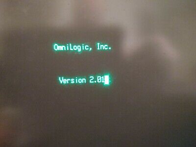
So I thought I'd dig out the ol' Omni4, which was made in the same year.
It took a tiny bit of effort to get the Omni4 booted, mostly consisting of acknowledging that my A-drive is flakey. Swapping it out with B did the trick, and I started reading the online help to figure out a triggering scheme.
I ran some really simple tests, just toggling a pin between its internal pull-up and ground... Seemed to work great!
Then I read [most of] the manual, which is thorough, and was so-generously scanned by a fellow I met through here years ago. (mine didn't have a manual).
Interestingly, the manual mentions at least twice that the disk should *not* be inserted during power-up, and *should* be inserted when the drive light is on. The claim is that CP/M is notorious for creating bad sectors if the disk is in during power-up/down.
As @ziggurat29 pointed out, this is probably more about the drive-electronics and electrical glitches than about CP/M, but either way, the Omni4 manual makes a big point of it twice.
I certainly had never worried about it before...
All those years ago when I backed-up its disk, I'm pretty certain I treated the machine more like I'd always treated a PC, when intending to boot from floppy, and put it in *before* power-up.
Aside from tgat, as surely I mentioned in the early log-entries here, when I dug the OMNI4 outta storage that first time, after numerous moves, I discovered its disk had been clamped in the read/write heads for easily the decade I'd had it, and possibly most of the decade it went unused before it was given to me... And... It booted as soon as I powered it up. And... Of course I went through several power-cycles at that time with the disk in...
Maybe that's part of the reason I had such difficulty extracting the sectors... Maybe a power-glitch toggled an MFM-encoded bit, somewhere...
So weird how that went... I tried *numerous* methods to try to recover the data... Oh the months... only eventually to essentially give-up and just run a script to repeatedly read each sector as many times as it took to get a valid checksum. I *really* did *not* expect that to work, but it did. Sheesh.
So, I suppose, maybe, in the realm of MFM-encoding, it's plausible such a power/write-glitch could've occurred *anywhere(s)* on the disk surface... including, plausibly, somewhere *mid*-"bit".
What would that mean, then? Well, *plausibly* since there's a clocking-reference at the beginning of each sector, and no guarantee of a clock alongside every "bit" thereafter, and thus a PLL is necessary to keep that clock ticking during the remaining "bits"... it's *plausible* that every time a sector is read it might actually *sample* the mfm-encoding (flux-transitions) at very slightly different timings... And maybe after a hundred tries it just happened to sample *past* or *before* the "glitch*...
I think I can see how it's feasible, anyhow. Especially with glitches that might occur in one bit-level vs the other... because, as I recall (was it bit='0'?) the *data* encoding is officially something like <flux-change, no-flux-change> but *also* is sometimes encoded as something like <no-flux-change, no-flux-change>, wherein the lesser-common encoding is especially used during the PLL-clock synchronization pulses *before* the data...
Hmmm...
So, I guess the point is that a single flux-transition might get mangled (or inserted?) in a sector, and it *might* be possible to read the data correctly, on random-ish occasion.
That *could* explain why the "brute-force" "just keep trying" approach eventually worked. Maybe... Heh!
Whoa, sidetrack.
Anyhow,
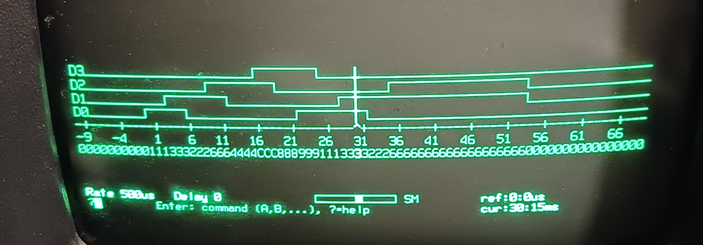
Yesterday I was stoked to see something, so hooked up the probes (for my first time?) to some circuitry... and... "bad sector."
Oddly, *after* I started being cautious about *not* having the disk in during power-cycles.
And, dare I note that there was no bad-sector (at least at that point in the program's loading) there the night before, nor the near decade since I wrote that disk? Heh.
(Thank Goodness I *did* go to all that effort backing up the original all those years ago! Now I guess we'll see how good my documentation is for writing a new disk).
.....
In other news:
I'd given-up on using the 5.25in drives that came with the machine in favor of 3.5in. This was such a weird discovery... because, surely, it would've become a common hack! It's almost that they *designed* 3.5in drives *to* be drop-in-compatible with 5.25in drives...
If I plug a 1.44MB drive in place of the old 390(?)KB drive, then use the old 720KB 3.5in disks (or put tape over the 1.44MB hole), it works fine-n-dandy.
As I recall the only jumper-change necessary was due to the weird PC-style Drive-Select scheme (with twist in the cable).
The key points were that A) my 5.25in disk stash was running low, B) I didn't have a spare low-density 5.25in drive to put in the PC (1.2MB drives weren't writing disks reliably-readable on the low-density drives) and C) I needed to use a laptop to image disks... Compatibility with available tools.
I'm *really* surprised how rare it is to find folk who replaced those 5.25in drives with 3.5in!
....
OK, so today's challenge...
The 486 laptop I'd been using to image disks is in sad shape. (rabbithole 3A).
And... The OMNI4 used some trickery to fit an extra sector on each track that newer PCs' floppy controllers are known to seldom be capable of working with.
I've got a box full of old motherboards, I think, still, if they made it through the last move... But that box *was* "dead" boards, where I had previously found a functional early pentium for this task, but apparently that machine did not make it with the last move... Abd, again, am I gonna go caseless?
...
Anyhow, thankfully it seems I still have a few 3.5in drives that might help.
Maybe one a deez dayz I'll wisen-up and throw a single "log entry" like this into my projects, early-on, and link it (singular!) in the project-description, or something, so it's easy for me to find, but doesn't flood the logs with a bunch of tiny notes-to-self... Especially annoying, because such things often pop-up months or years after I last worked on the project, and often the last log was worthy of being recognizable as the last directly-related to progress. I dunno.
Anyhow:
Notes-to-self:
avr-libc: util/crc16.h
*looks like* some decent code and references regarding the CRC used on floppies.
(Which, for all who aren't in the know, was a deep rabbithole the OMNI4 led me into, that resulted in the discovery that many *respected* references on the matter turned out to implement it *very differently* than they *explained* it. [schematic diagrams using shift-registers did *not* match the code implementations]. And, the further discovery that that disconnect seems to exist in MANY references on LFSRs, in general... which may very well be why I had so much trouble implementing one in my capstone class ~20 years ago. BUT, while working on the OMNI4, I finally noticed that disconnect in numerous resources, and agonizingly convinced one to correct it... heh. So here are some more direct references I might one-day compare my findings to.)
While I'm very *pro* keeping this thing in original form... I haven't really found much use for it. (Mostly, maybe, due to so many project-ideas, and "real life," whatever that is).
...
Weird idea... first some background...
This interesting article came up about an electronics-related archaeological endeavor...
Following Adam Fabio's rendition of the story, I was running through the ideas of what the mystery-chip could be, but didn't quite get there on my own... OF Course! A DMA controller! How else would a system of that vintage keep up with the timing demands of sampled audio?
Which led me to the observation that... Heh, that was one of the big-learns from my [our] archaeological endeavor with this system, the Omni4... DMA controllers running the bus and RAM far faster than the Z80 CPU could... at a time when, frankly, it was darn-near shocking to look back on and believe such speeds were possible. 20MSPS!
...
For a brief moment I considered the possibility the Omni4's logic-analyzer add-on card (being an otherwise stock Kaypro machine) might just be capable of doing for the Kaypro what the card in the article did for the AppleII... Heh!
This is my brain, and why I have so many project-ideas and actually get to doing so comparatively-few.
I'm no musician, anyhow... But I know a thing or two (built most my career around) MIDI, so I suppose adding a keyboard would be a snap in comparison to writing the software...
Heh. The original software-architect for the AppleII product was, apparently, pleased to be approached about his long-forgotten masterpiece... Heartwarming.
Wonder if he'd cough-up sourcecode. Heh!
6502 assembly, maybe? What a friggin ridiculous undertaking this would be... especially for a long-forgotten, if ever even recognized, board that only seems to exist in two machines in the world, OTOH... OTOH...
...
The "Heartwarming" aspect of this article is really what gets me. There's no particular reason to go down a path like they did. Nearly any keyboard can be connected to nearly any computer these days, and loaded-up with one of probably dozens of softwares to acheive the same as this setup, and probably far more.
OTOH, these folk found the time and cause to remember some other folks' long-forgotten hard work... And part of my early draw to electronics and software is its duplicatability, specifically in the interest of its longevity.
Some folk got together long ago and created their "baby"... It wasn't the best of the best, by any means. Sure, the Fairlight won that competition hands-down. But, here, these folk, complete strangers to the originators, have gone out of their way to make sure that forgotten baby has offspring... Beautiful tale.
...
I have no idea how that fits with the Kaypro/Omni4 idea, except in that plausibly it wouldn't be difficult to reproduce that card, similarly. But, well, 20MSPS logic analyzers sized to fit 5.25in floppies aren't particularly desireable nor useful, even to the hardcorest test-equipment collectors... But maybe it's just a matter of software and a tiny add-on (for output) to turn it into something more... an alternate timeline where Kaypros were competitive with AppleII's competitiveness with the Fairlight. Heh!
But, see, it could be more than that... Card-interfaces back then were quite simple... Really not much more than tapping off the CPUs' memory-bus... So, I mean... It wouldn't be implausible to use either of these cards in *any* 8-bitter system (even, say, an AVR)... with some software-generalizing and new plug-ins...
OK, yeah, a bit carried-away. But, not implausible. And, for an hour or so, there, I was pretty excited about the possibilities. Enough to start writing about it, anyhow... with two friggin' thumbs. Heh!
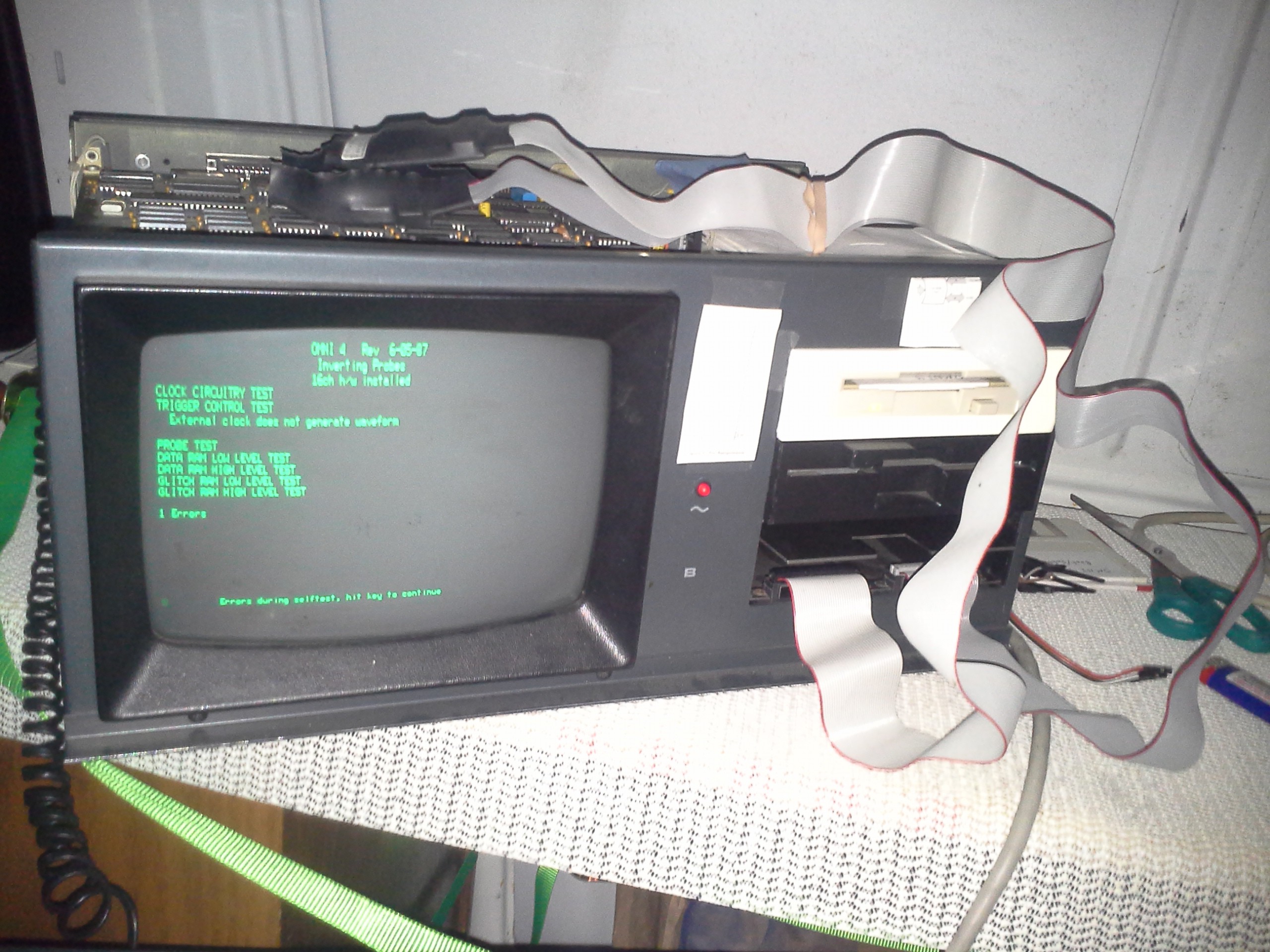
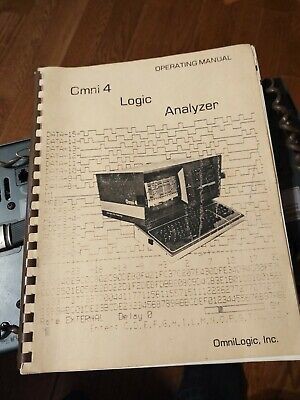
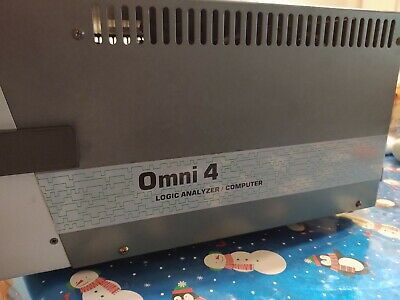
Dominic--who happens to be selling the only other OMNI4 I'm aware of in existence--very kindly scanned and sent me the user manual [possibly the only in existence] for posterity!
A copy is in the Files section.
BTW, Dominic's been quite awesome taking the time to do this and more. If you're intrigued by the OMNI 4, consider purchasing it from him at:
If you decide to purchase this unit, please keep in touch, and consider joining the 'team' here to contribute!
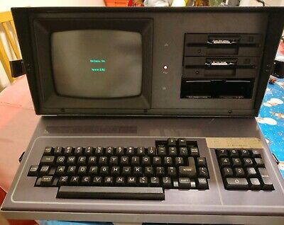
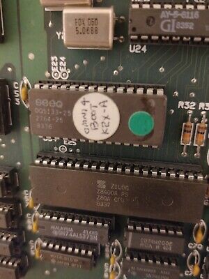
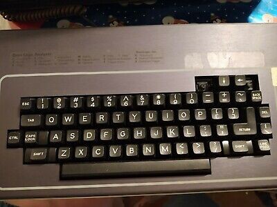
This unit differs from mine in at least one notable way; mine doesn't say anywhere on it that it's a Kaypro 2x. @ziggurat29 had to figure this out by looking up Kaypro motherboards!
[Also, an odd note, apparently when using 'cpmtools', one must select 'kpiv', even though the Kaypro IV is an entirely different beast(?)]
[TODO: take similar shots of mine for side-by-side.]
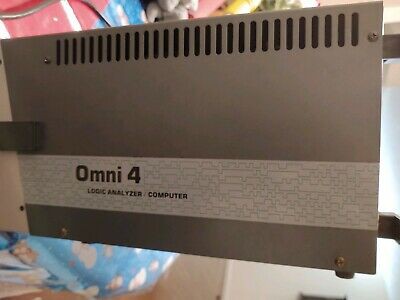
This appears to have the drop-down door type latch floppy drives, whereas mine has the rotating lever-latch.
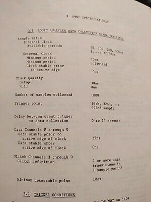
A manual!
"Kaypro 2x" heh, that'd've been handy
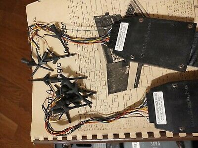
Hmmm, my pods are merely heatshrunk, and their cables merely ribbon cables. [And, crosstalk/interference was an issue]. Seems even more plausible, now, mine might've been a prototype?
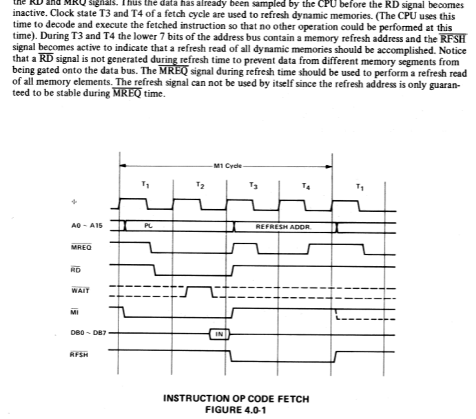
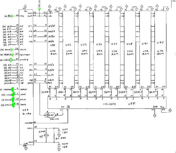
So, the question, earlier, came up regarding how the DRAM gets refreshed, if the /REFRESH pin is N/C (which it appears to be, according to the schematic).
and dammit if I didn't have a long write-up on the matter, and lost everything after this point. So, I guess I'll get to the point.
There's really no *need* for the /RFSH signal. At least with typical DRAMs. Basically, a row in the DRAM is refreshed whenever a row is accessed. And for a typical Read/Write operation, the row is accessed first, then the column, then the Read/Write signal is sent. So, the row gets refreshed with every read/write access.
So, why not treat *every* address placed on the address-bus, accompanied by /MREQ, as a Row AND Col access, as though for a read/write? And... now I'm pretty sure that's what happens.
Simple. And I'm betting the custom chip doesn't contain any specialized logic regarding refresh.
----------
There's still the issues of BANK and /PROMCS, and how those are related to the DRAM... My guess, again, is that *every* address-access on the Z80's address-bus, accompanied by /MREQ, accesses a memory-location in the DRAM (even, for instance, when the ROM is being read).
BANK is controlled by a bit on the "system port" register... That, as we understand, chooses whether to do memory-accesses from the ROM or the RAM. So, e.g. during boot, BANK directs it to the ROM, then after boot, its directed to the RAM where the OS is stored, etc. (There's some debate as to whether the "BIOS" in the ROM is accessible to applications once the bank has been switched to RAM... E.G. if there could be, say, routines in the BIOS for displaying characters on the screen, could that be called from a user-application, switching into the ROM for execution, then back into the RAM for the next portion of the user-application? I'm sure there are ways, but they may not be pretty... e.g. storing *pieces* of the same code in both ROM and RAM, at the same locations... I'm sure I can find out with further analysis of Ziggurat's ROM disassembly).
So, obviously, when BANK is set to ROM, /PROMCS gets activated with /MREQ, but /XENRAM does not. But, then, when the ROM is executing (during boot), the RAM still needs to be refreshed... so its still feeding *every* address-access to the row/col system... Which is fine for /RD, since /XENRAM is disabled and therefore the data in the DRAM is not written to the data-bus...
But what about Write...? /WR is not gated through the custom chip, it goes *straight* to the DRAM!
Ah hah!
Write... Never Happens to the Read ONLY Memory.
OK-then...
Now this leads me to the question of how the ROM can access RAM, for storing variables, etc.
In what I've seen of Ziggurat29's disassembly, it seems the stack-pointer is set-up in a high-address, e.g. 0xff00... and it seems most other variables are stored up there, as well...
So, then, BANK only switches between ROM and RAM in the *lower* addresses, and always accesses RAM in the higher ones... simple enough.
And, again, by treating the RAM as though it's being accessed even when the ROM is, but gating the RAM's /RD signal (/XENRAM), it still gets refreshed.
This custom chip is starting to seem quite simple, really... a few gates.
(As Ziggurat29 pointed out a while-back, the 2x motherboard uses this custom chip, but the earlier motherboards are similar in design but use discrete logic instead... I've been meaning to look at those, but haven't yet. All these ramblings are from the perspective of treating it like a black-box... I guess it's kinda like doing math homework where the answers are in the back of the book... should I go look?)
-----------
Whoa Whoa Whoa!!!
that /WR signal is *directly* connected to the DRAM chips! And they don't have Chip-Selects! That's fine for ROM... but...
What the heck happens during an I/O write!?
... "/CAS is used as a chip select activating the column decoder and the input and output buffers."
So, maybe I'm mistaken in the above assumptions that /RAS and /CAS are *always* strobed... Maybe only /RAS is, and /CAS is only strobed alongside /MREQ... oy!
-------
I do, in fact, have a logic-analyzer occupying *exactly* the same space as the circuit I'm curious about... And that logic-analyzer, in fact, samples quite a bit faster than the circuit I'm curious about... THAT would be the logical approach.
------
This looks quite handy, though I think it's for a KayPro 2, rather than 2x...
1) An image-search for '"Omni 4" "Logic Analyzer"' results in many hits from this project-page... pretty cool. OTOH, it's quite strange, saying that many of the images are "4-5 days ago" that were actually several months ago. (is it 4-5 days ago that Google crawled on 'em?)
2) A resulting-image doesn't show anything related to the OMNI4... so I clicked through to the page to see what Google thought made it relevant... Apparently MAME now comes with the OMNI4 ROM (?!)
 Eric Hertz