 Edward Viaene
BenchPod v2
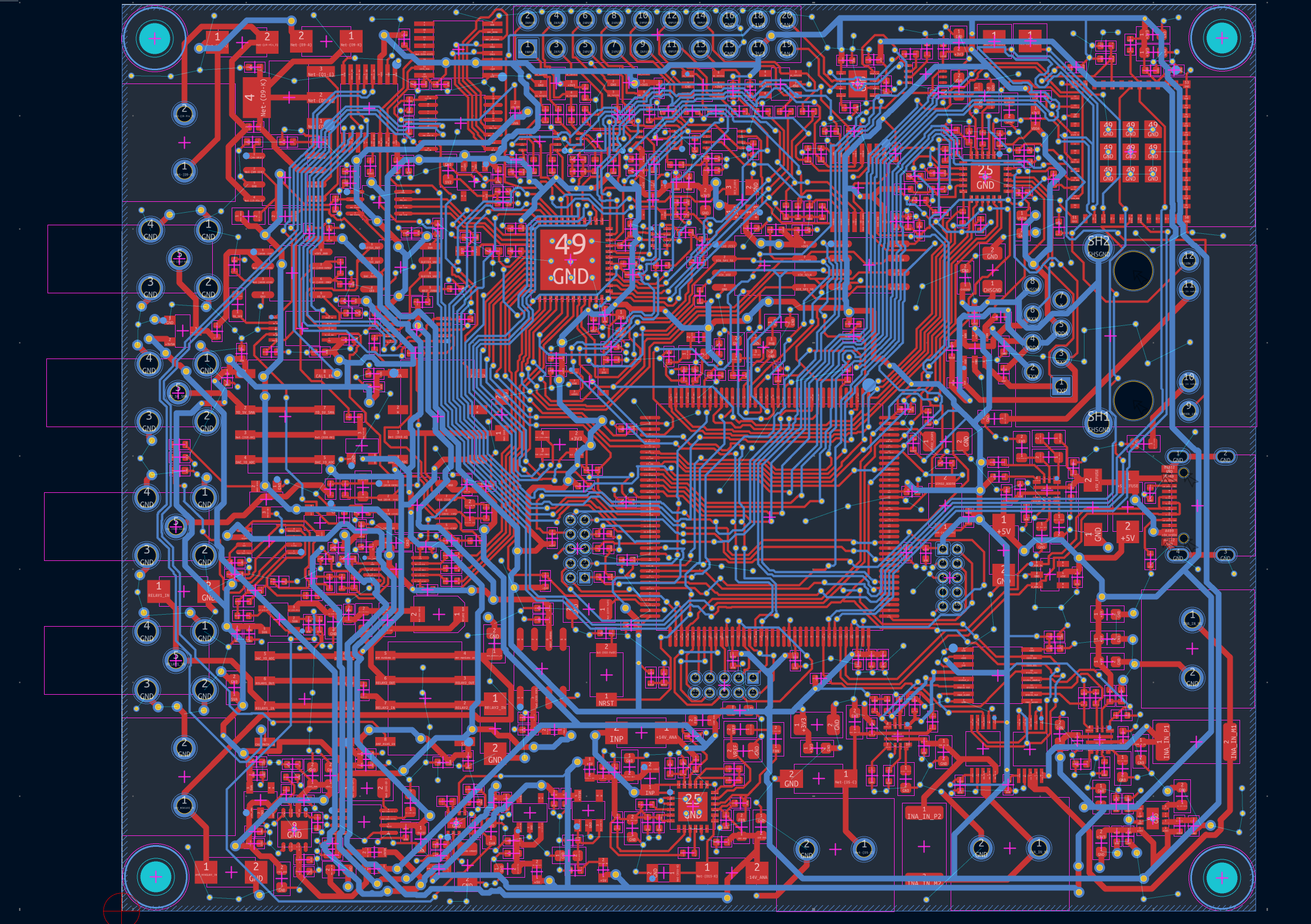
v2 is a complete redesign from v1. The goal is the same — a single board that consolidates the instrumentation you'd normally spread across a bench — but the architecture is substantially upgraded based on what v1 taught us.
Compute
The main MCU switched from RP2350B to STM32H563ZIT6 (LQFP-144). The primary reason is native Ethernet: the H563 includes a 10/100 MAC that talks directly to a LAN8742A PHY, with an HR911105A MagJack handling the physical port. The STM32 also gives us six hardware SPI buses, hardware crypto, and a more mature ecosystem for the kind of SCPI-over-TCP instrument control we're building toward.
The iCE40UP5K FPGA returns from v1, again with its own W25Q64 flash for autonomous bitstream load at power-up. In v2 it takes on more: logic analyzer capture, ADC/DAC orchestration, and a planned SWD finite state machine for DUT programming. An APS6404L 8MB QSPI PSRAM sits alongside it for capture buffering.
WiFi is handled by an ESP32-C3-MINI-1, now explicitly treated as a dumb WiFi NIC running esp-hosted or AT firmware. The STM32 manages it over SPI.
Analog input
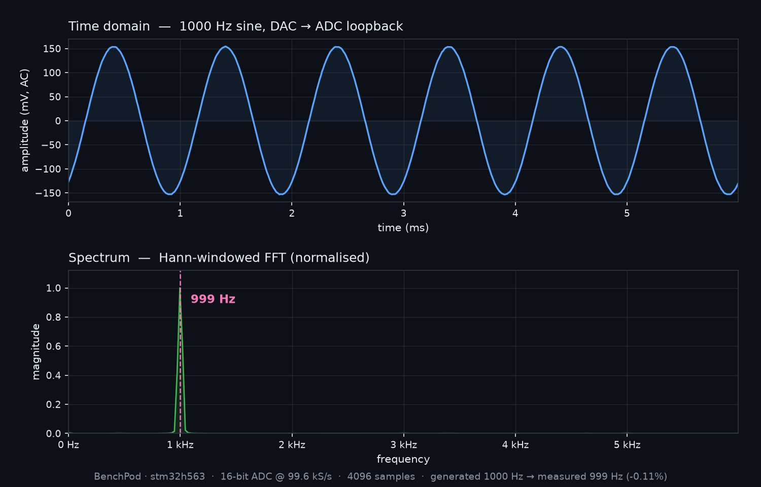
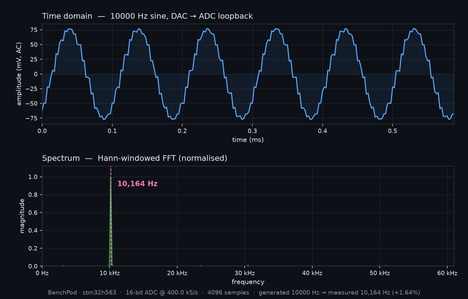
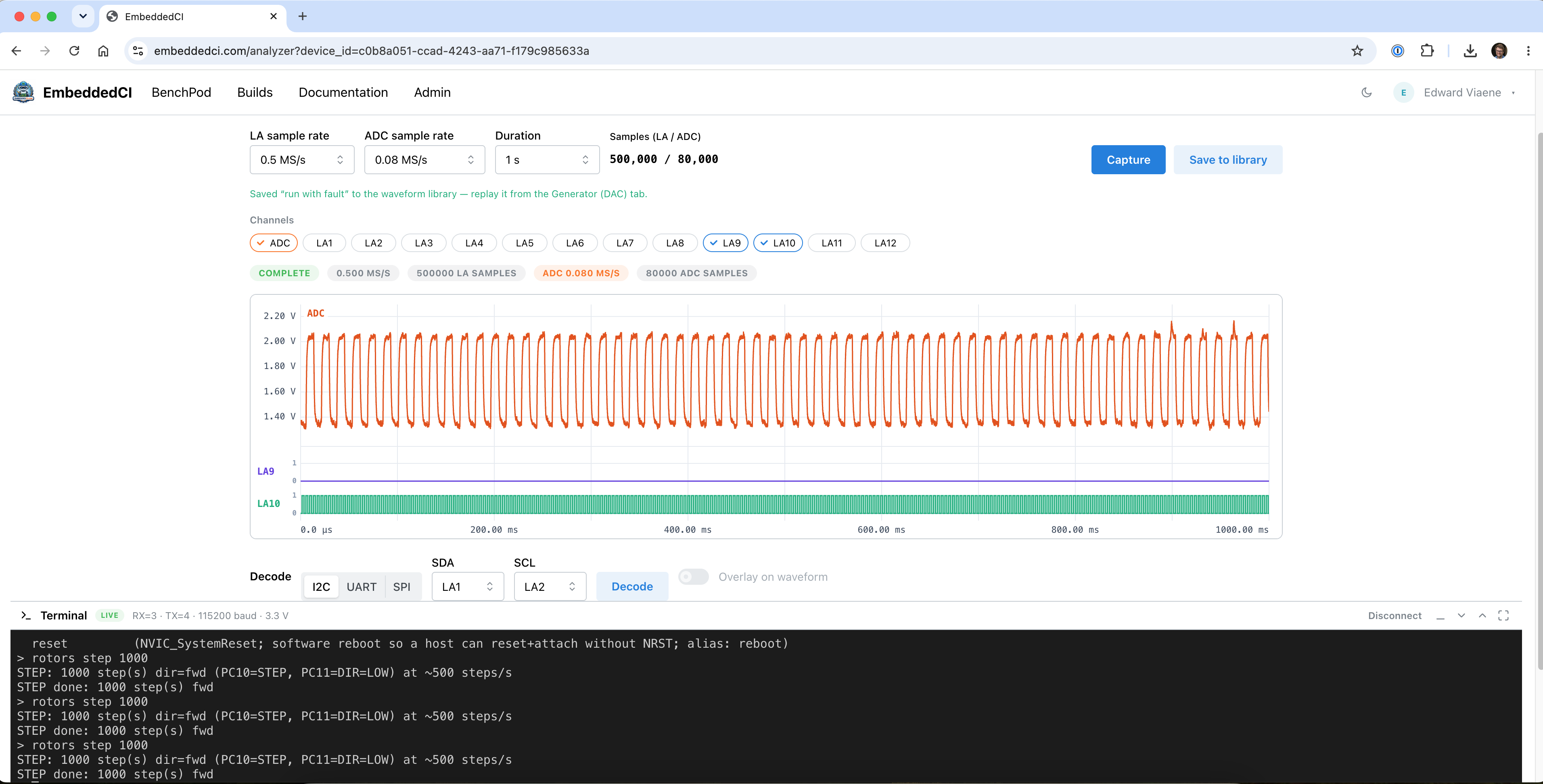
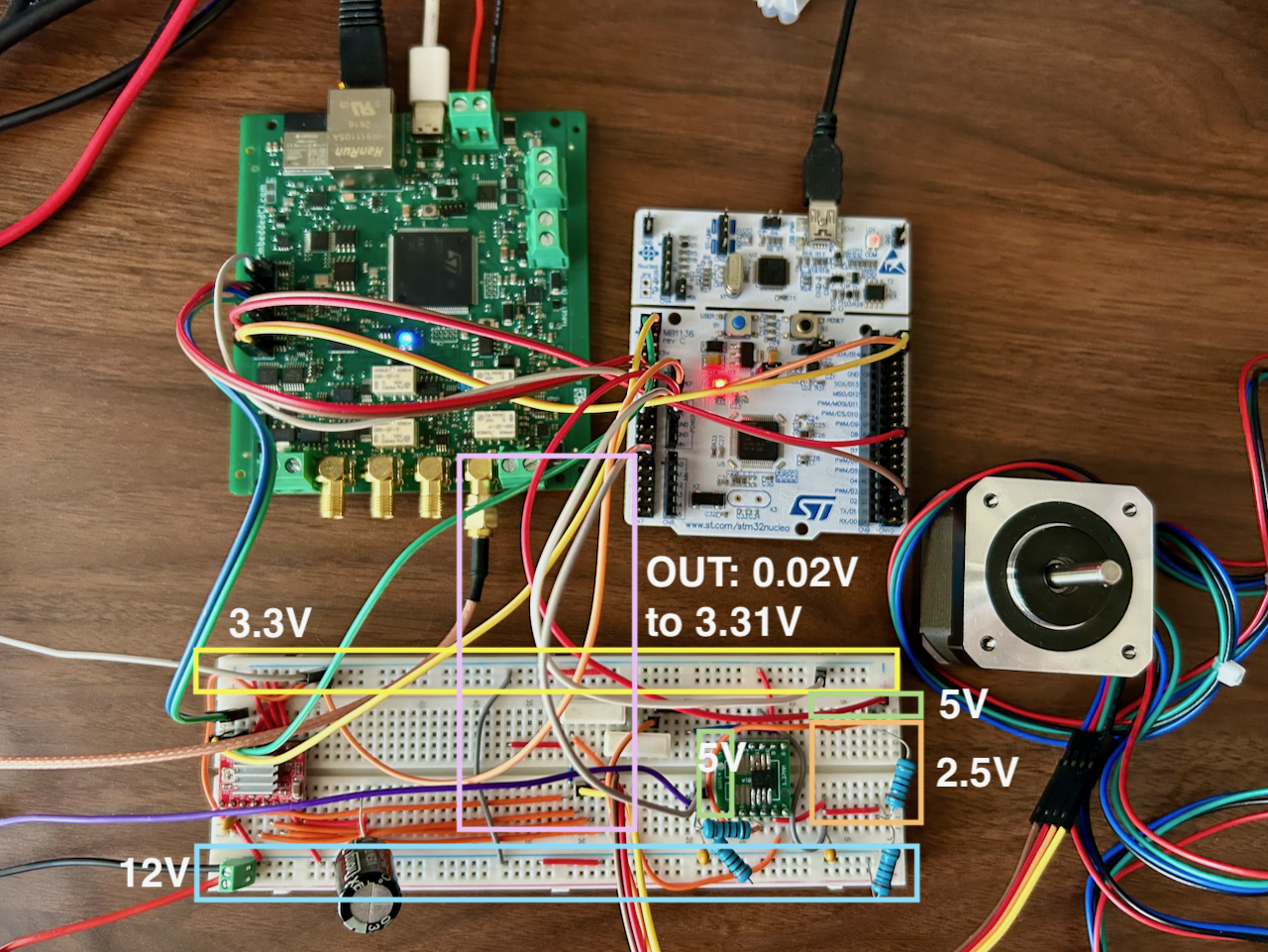
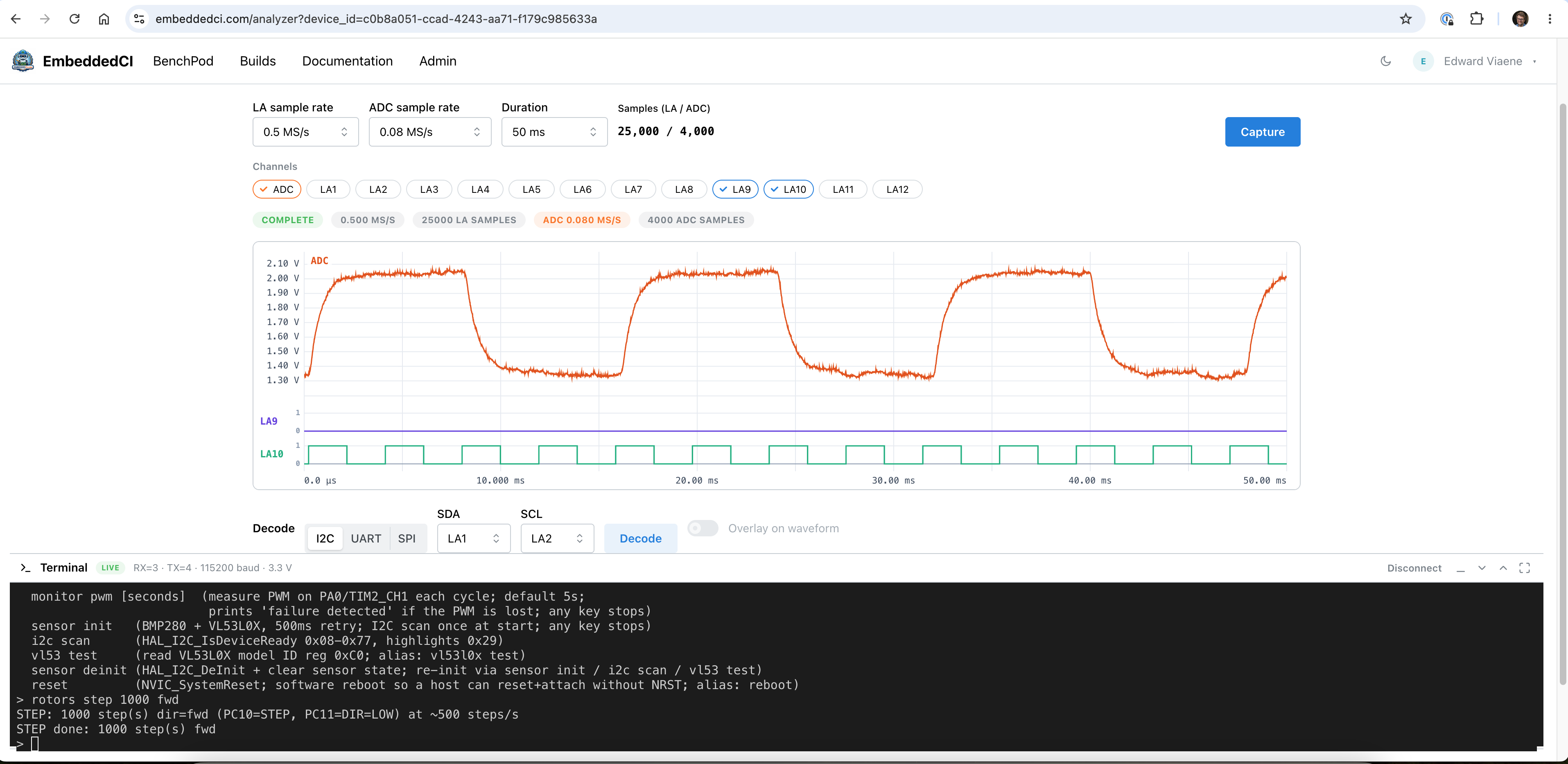
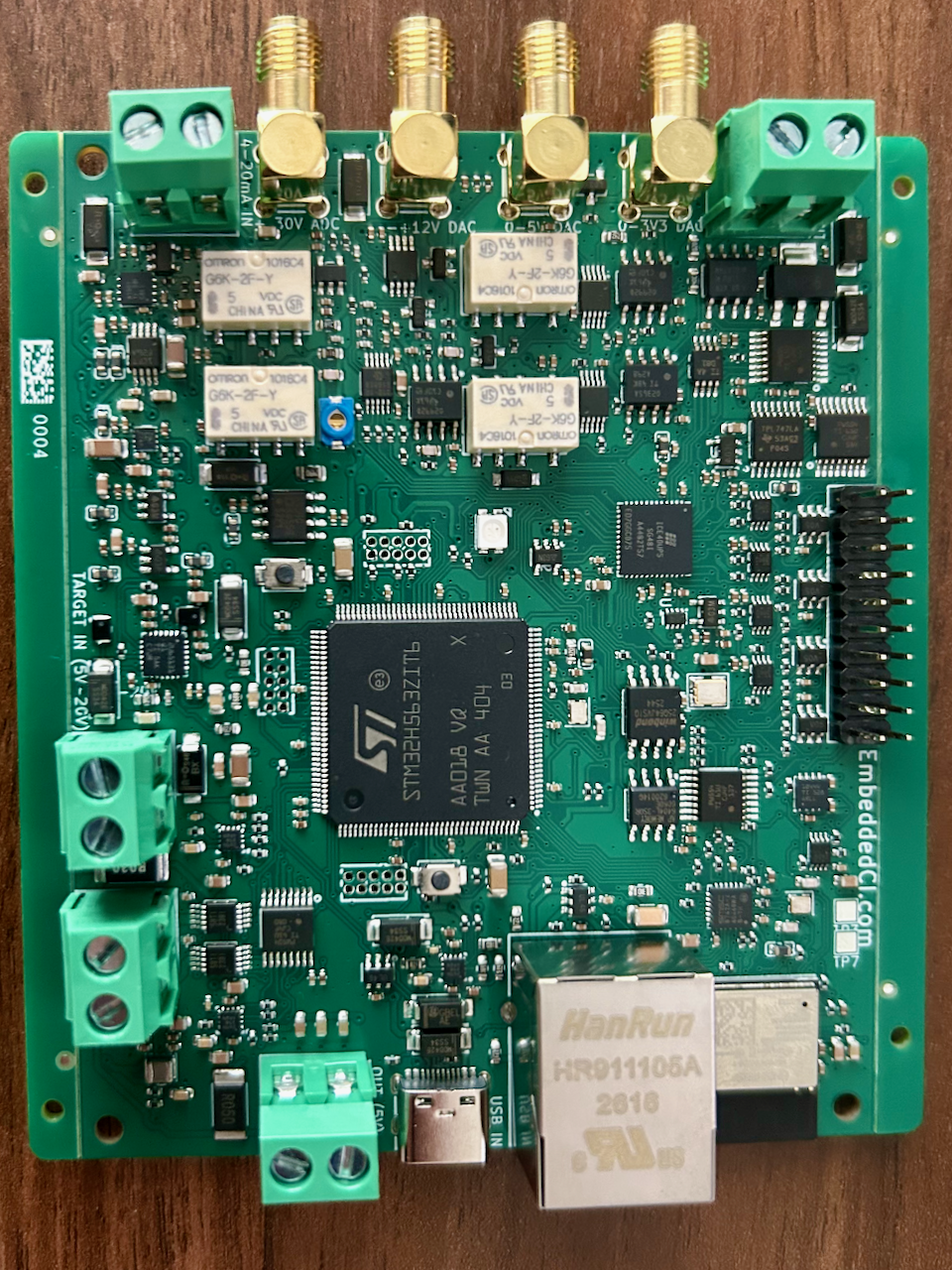
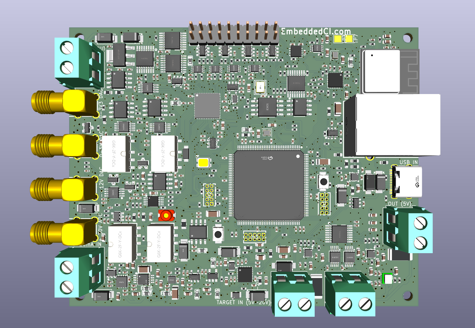
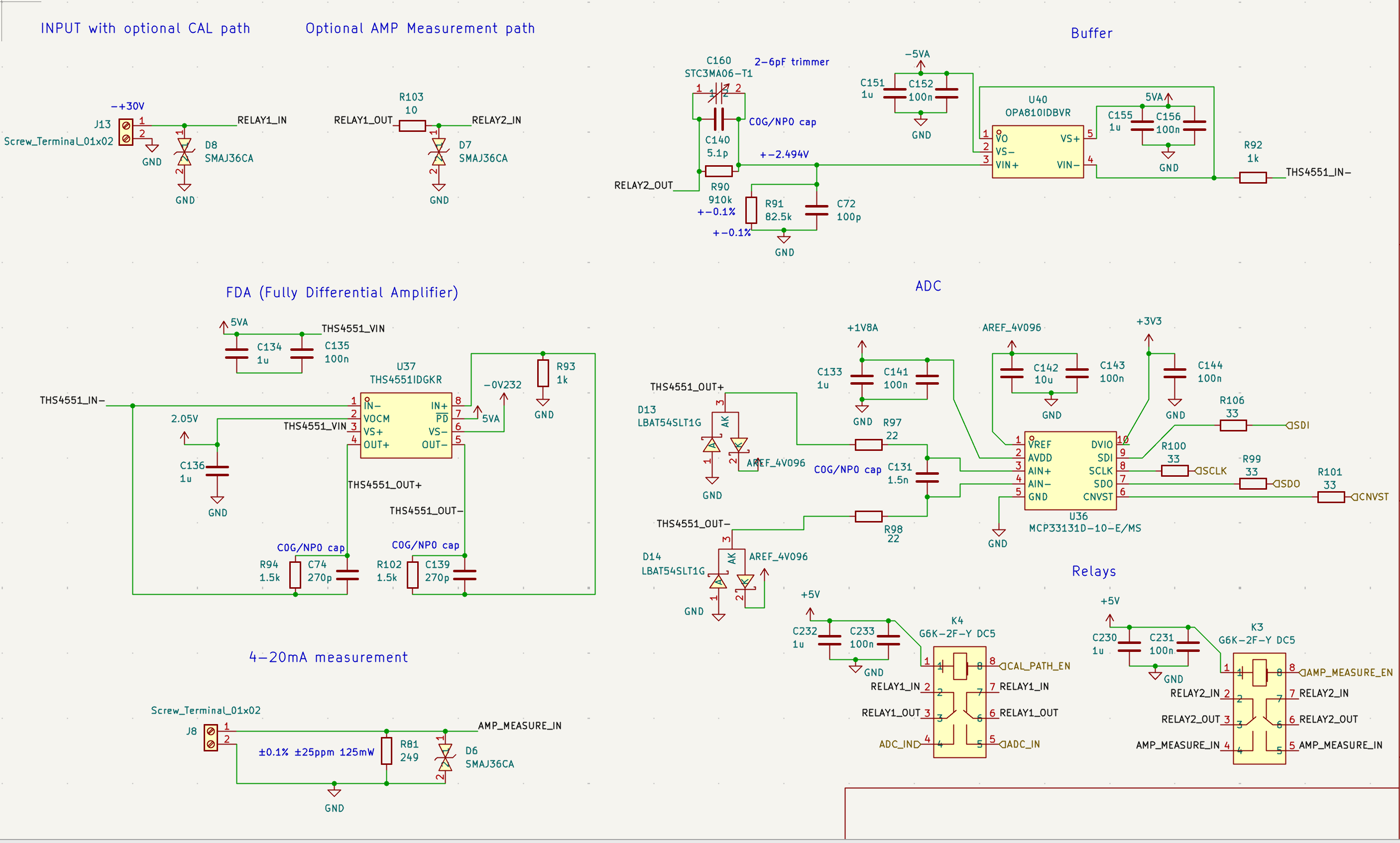
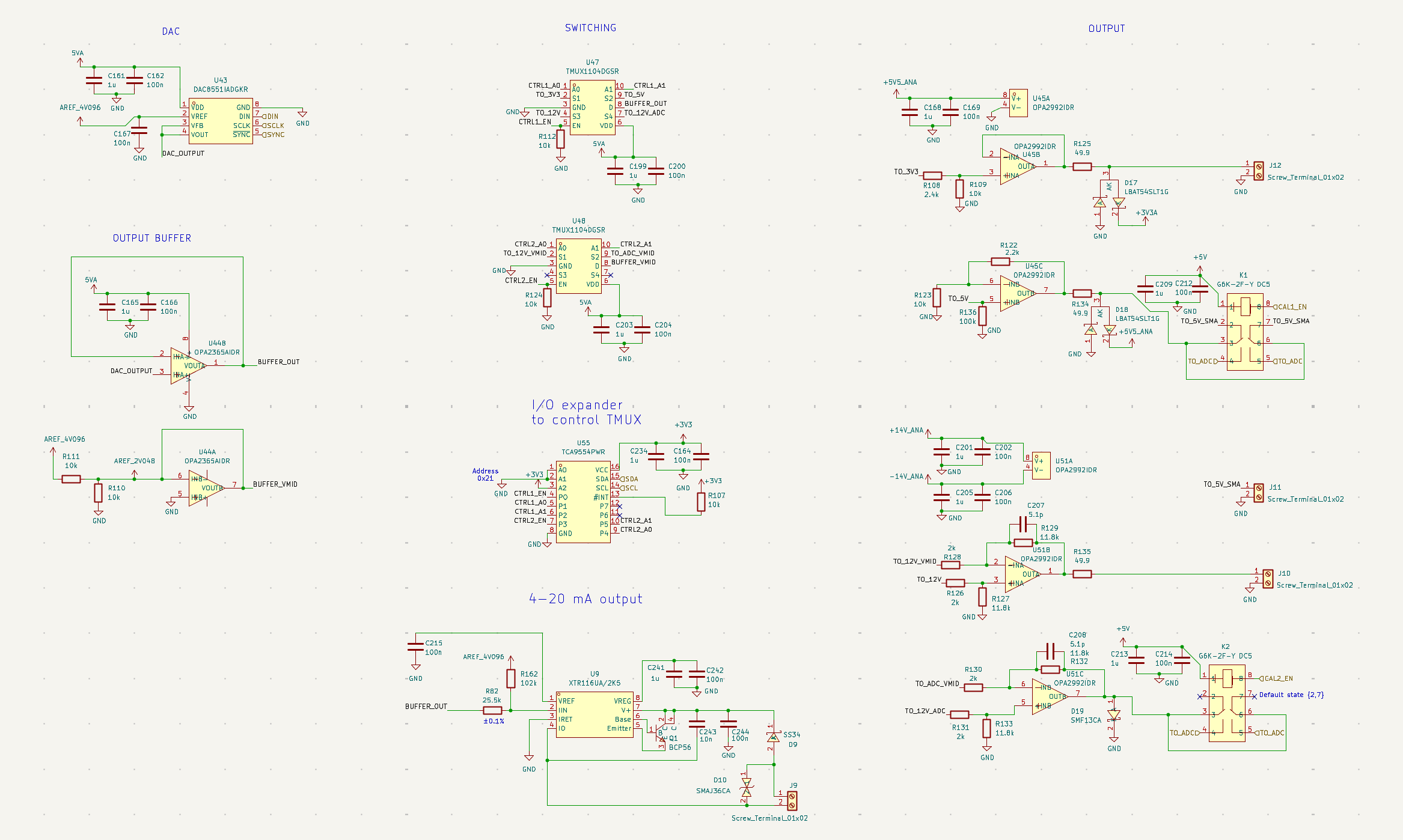
The analog front-end was the weakest part of v1. v2 replaces the 8-bit, 60 MSPS ADC with an MCP33131D-10, a 16-bit SAR ADC running at up to 1 MSPS. The signal chain is: a compensated ÷12 resistive attenuator, an OPA810 input buffer, a THS4551 fully differential amplifier driving the ADC, and an ADR4540 4.096V precision reference. Input protection is LBAT54SLT1G Schottky clamp pairs. Connectors are SMA (RF3–RF6) instead of BNC.
A relay-based calibration injection path uses four G6K-2F-Y reed relays driven by a TPL7407LA, allowing the DAC output to be switched into the ADC input for in-situ calibration without external connections.
Analog output
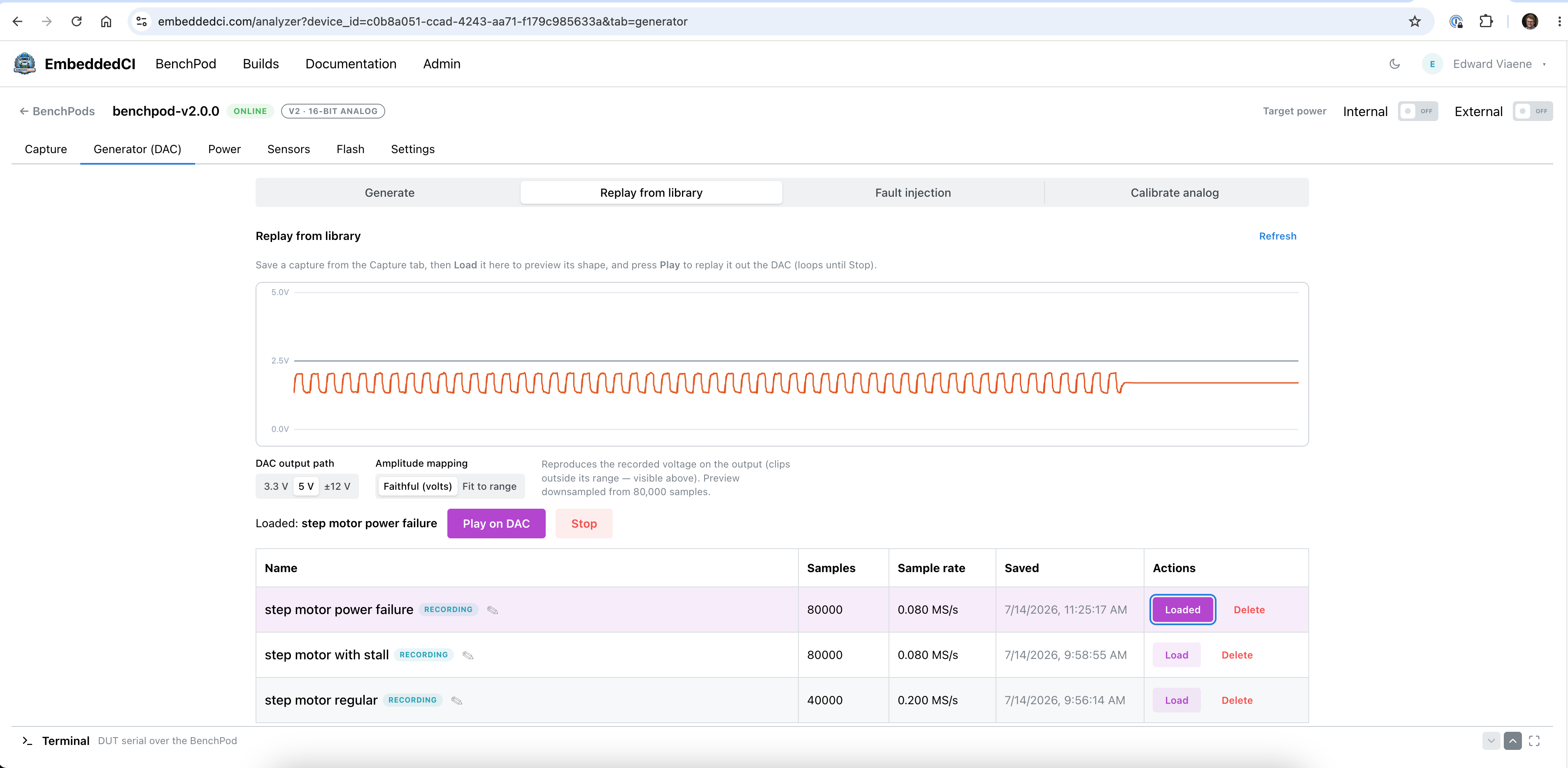
The DAC is a DAC8551 (16-bit SPI), buffered through OPA2992 op-amps with TMUX1104 analog mux routing. A TPS65131 dual-rail boost converter and LM27761 negative charge pump generate the bipolar supply rails needed for rail-to-rail output swing. An LM7705 provides the negative supply bias for the op-amp output stages. The XTR116UA handles 4–20 mA current loop output with a BCP56 pass transistor.
Power
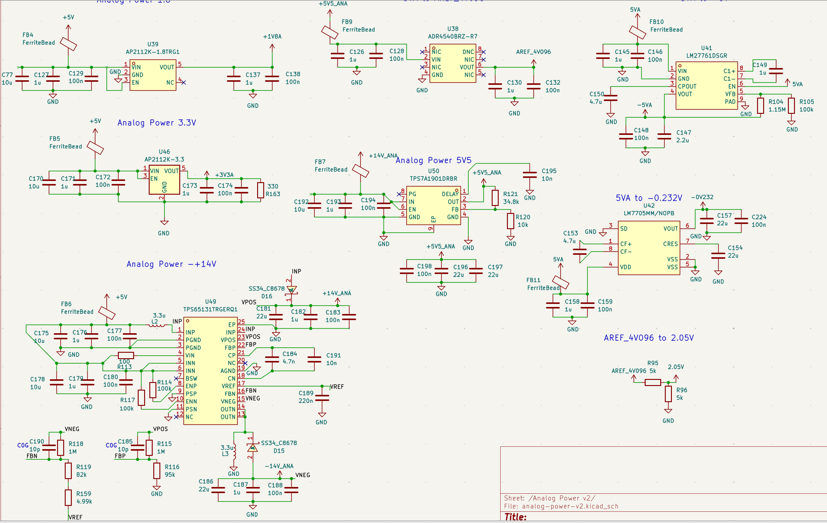
Three TPS259470A eFuses protect the switchable power paths. INA238 monitors (replacing v1's INA219) track current and voltage on each rail. The internal power tree uses a TPS82130 3A MicroSiP buck for 3.3V digital, AP2112K LDOs for 1.2V, 1.8V, 2.5V, and 3.3V analog rails, and a TPS7A1901 LDO for the precision analog supply. A TPS2116 handles power mux for input supply selection.
Connectivity and DUT interface
Ethernet via RJ45 (HR911105A) is the primary host interface. USB-C remains for firmware updates and initial config. The SN65HVD230 CAN transceiver returns, now wired to the STM32 directly. DUT-facing I/O includes I2C, SPI, UART, and GPIO, with SN74LVC2G66 analog switches for switchable pull-ups and SRV05-4 TVS arrays for ESD protection. Four TCA9554 I2C I/O expanders (replacing v1's single PCA9555) add GPIO without burning STM32 pins.
 Patrick Van Oosterwijck
 marble
 Luke Valenty
 Paul Andrews