Edward Viaene
-
v2.0.0 Is Being Produced
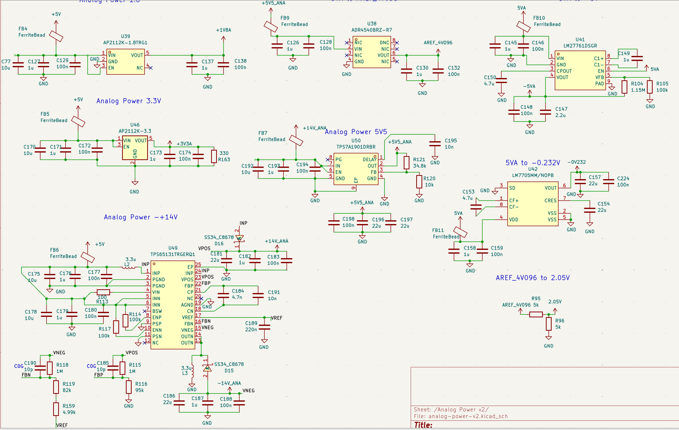
06/19/2026 at 15:00 • 0 commentsFinalized v2.0.0 and ordered it on JLCPCB (the new schematic is under files). A few notes
- PCBA standard is needed for ESP32, I knew that from the v1 version, but when you have more components, at some point the benefit of PCBA economy will disappear once you have a lot of extended components. This is because it's 3 USD per extended component in economy, but 1.5 in standard
- The RGB LED I picked needs some special treatment, which is another ~10 USD on top of that, and also bumps you out of PCBA economy
- The combination of lots of extended components and the ESP32 (for WiFi) makes, in my case PCBA standard roughly the same price (it's perhaps 10 USD difference)
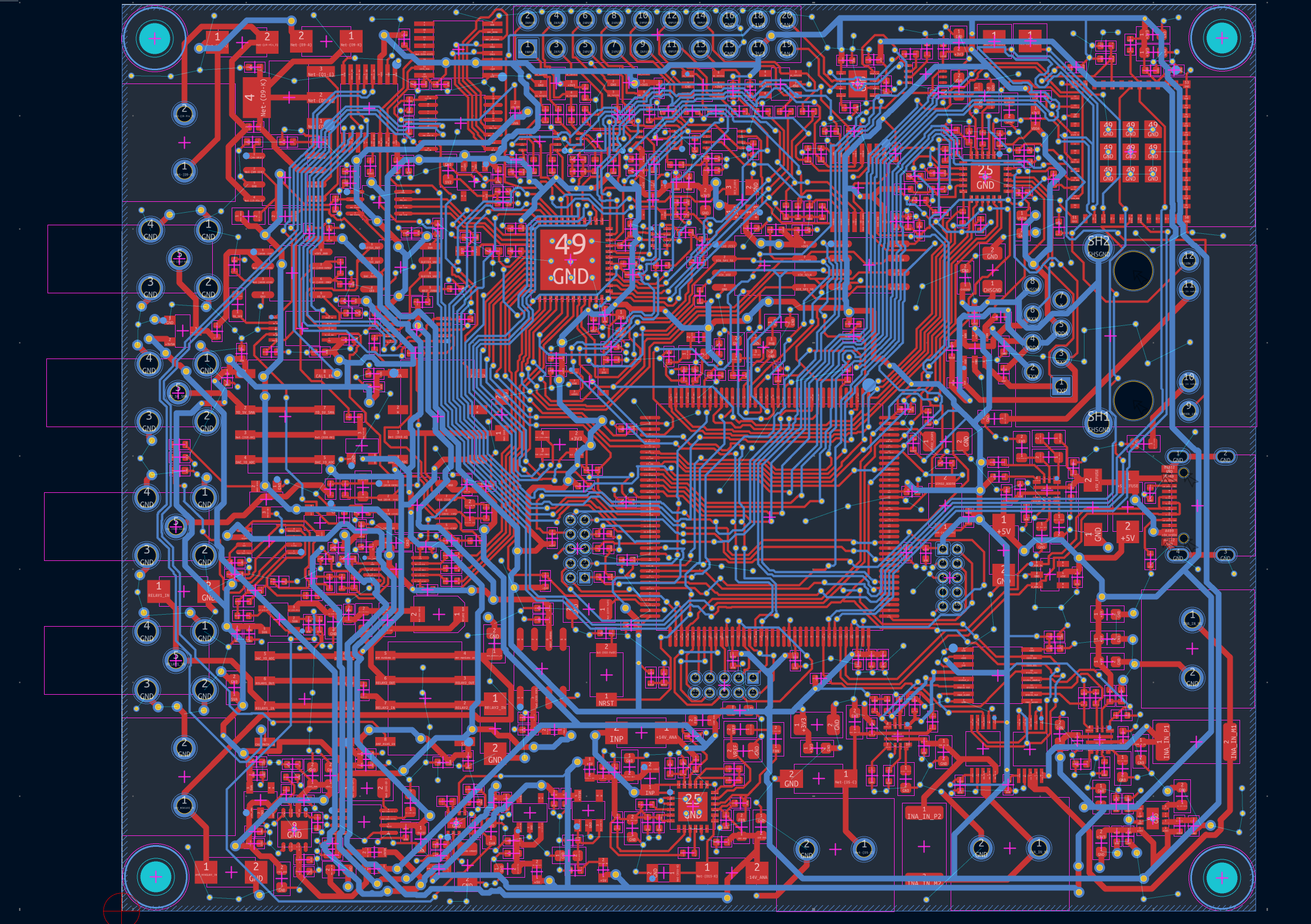
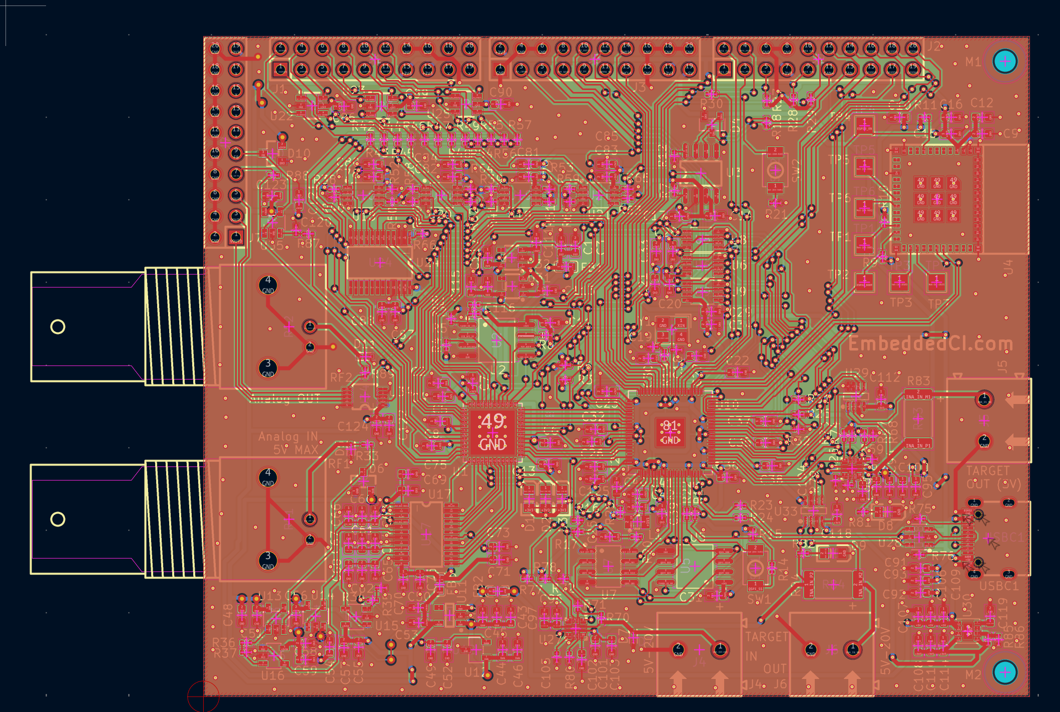
There are lots of components in v2.0.0, but the board size is the same. On multiple occasions, I wondered about expanding the board or going to more layers. More layers are much more expensive, so a bigger board would be a better solution. Still managed to route everything with the same board size. Almost all the analog path is routed on top. The power at the bottom. For the digital path, it's more mixed, but that should be OK. Here's a screenshot of the wired PCB. Left is analog, middle and right is digital. I removed the ground fill to make it more readable.
![]()
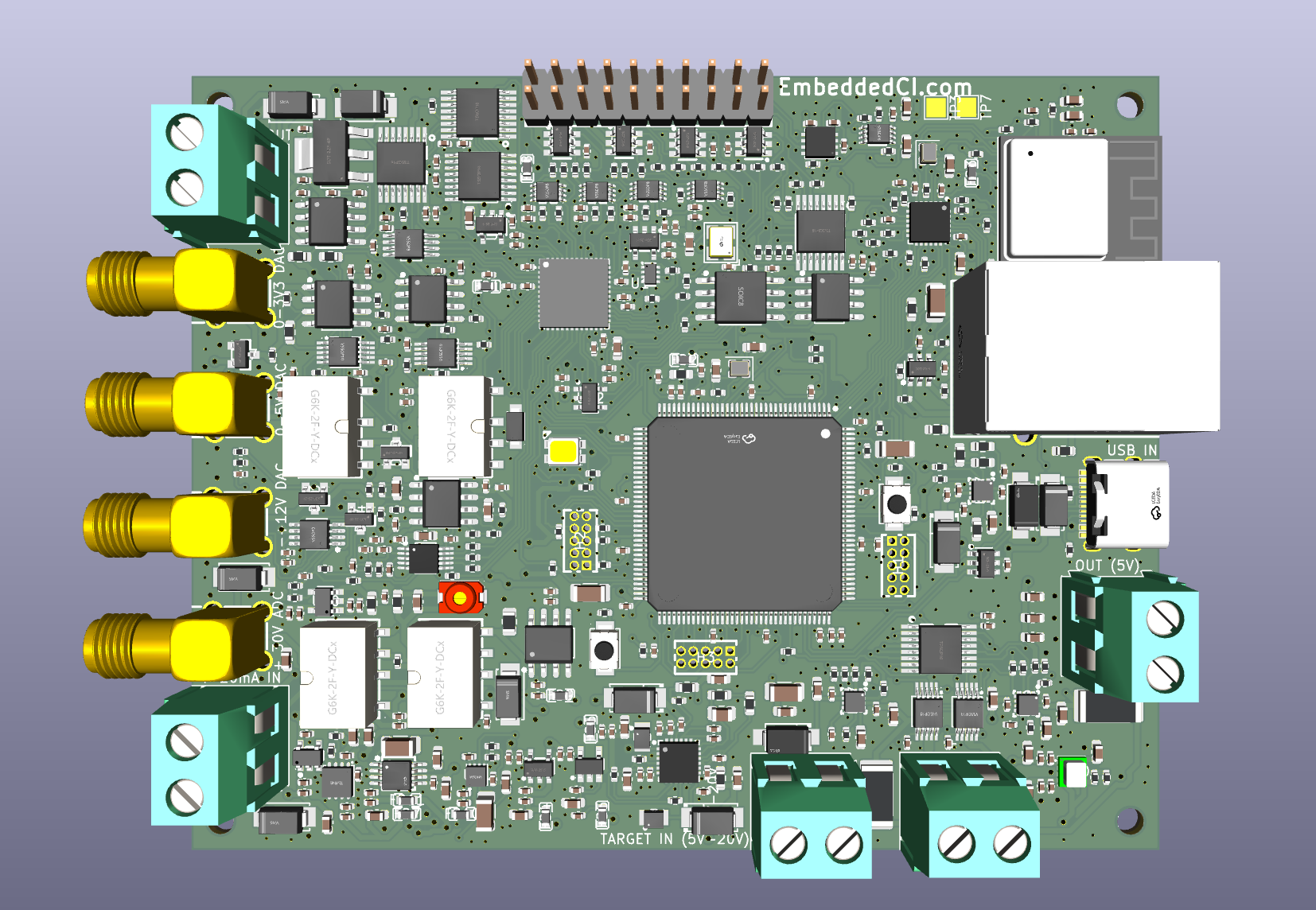
Here's the 3D overview. I picked SMA for the analog path (ADC / DAC) and screw terminals for the 4-20mA measurement and output. And yes, this STM32 is huge.
![]()
The difficulty with wiring the STM32H563 is that the pins are scattered across multiple protocols. RMII is on all sides, SPI is on all sides, so there's no perfect orientation for the chip. That quickly translates into trying to get all these traces from the ESP32 and RMII down to the STM32 and wiring it up from there.
-
Analog v2
06/16/2026 at 13:38 • 0 commentsStill working on the v2 version. Currently doing component placement, which means that (hopefully) the schematics are not going to change much anymore. What analog looks like right now:
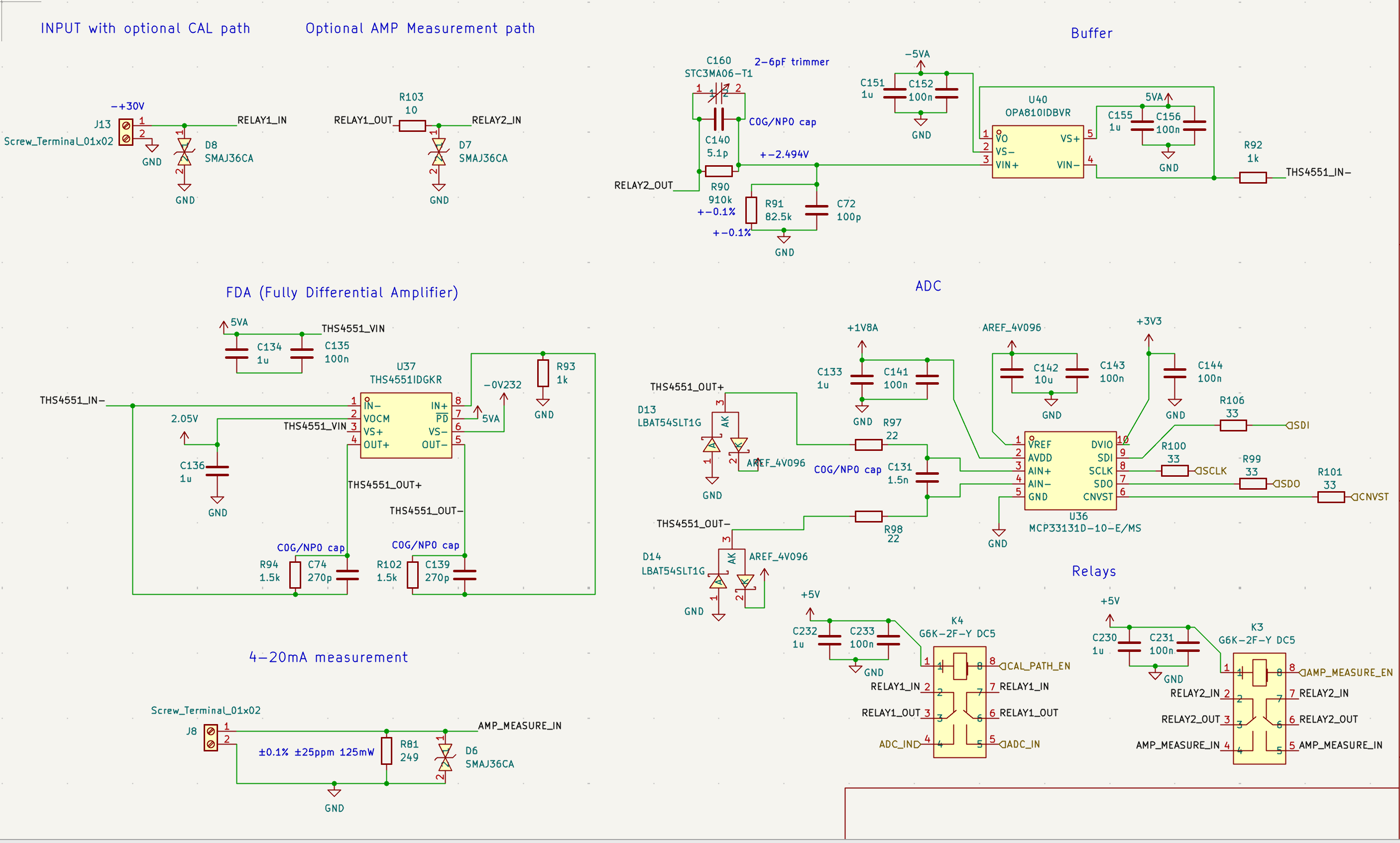
- ADC: +-30V input, OPA810 buffer, THS4551 Fully Differential Amplifier, and MCP33131D-10 as ADC (1MSPS, 16 bit). That is ~400 kHz usable signal bandwidth
- A 4-20mA measurement path can be switched with a G6K-2F-Y relay. It'll connect before the 12:1 divider and reuse the same ADC
- For calibration, there's also another G6K-2F-Y relay that can disconnect the input path and connect the DAC so that we can calibrate the DAC to ADC path
Here's the ADC schematic:
![]()
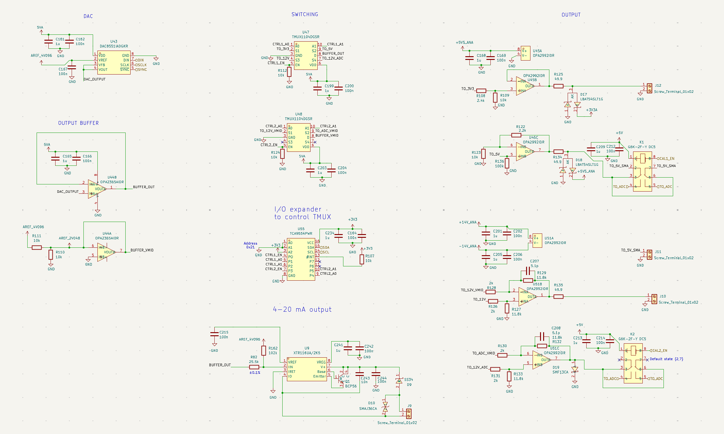
The DAC is a 16 bit DAC8551 with an OPA2365 buffer. I have a few TMUX1104 that can switch the path to different voltages: 0-5V, 0-3V, and -+14V. The -+14V is the path that can output to the ADC for calibration.
There's also a 4-20mA output from the DAC. There's another relay that can switch between outputting to the regular path or to the 4-20mA output path.
The DAC schematic:
![]()
Lots of parts, which means lots of loader fees at JLC, so let's hope it doesn't need many respins! There are 8 different voltages to work with in the analog section:![]()
-
v2: stm32, Analog, ethernet
06/11/2026 at 18:48 • 0 commentsWorking on the v2 with STM32, improved analog and Ethernet. A few thoughts/updates:
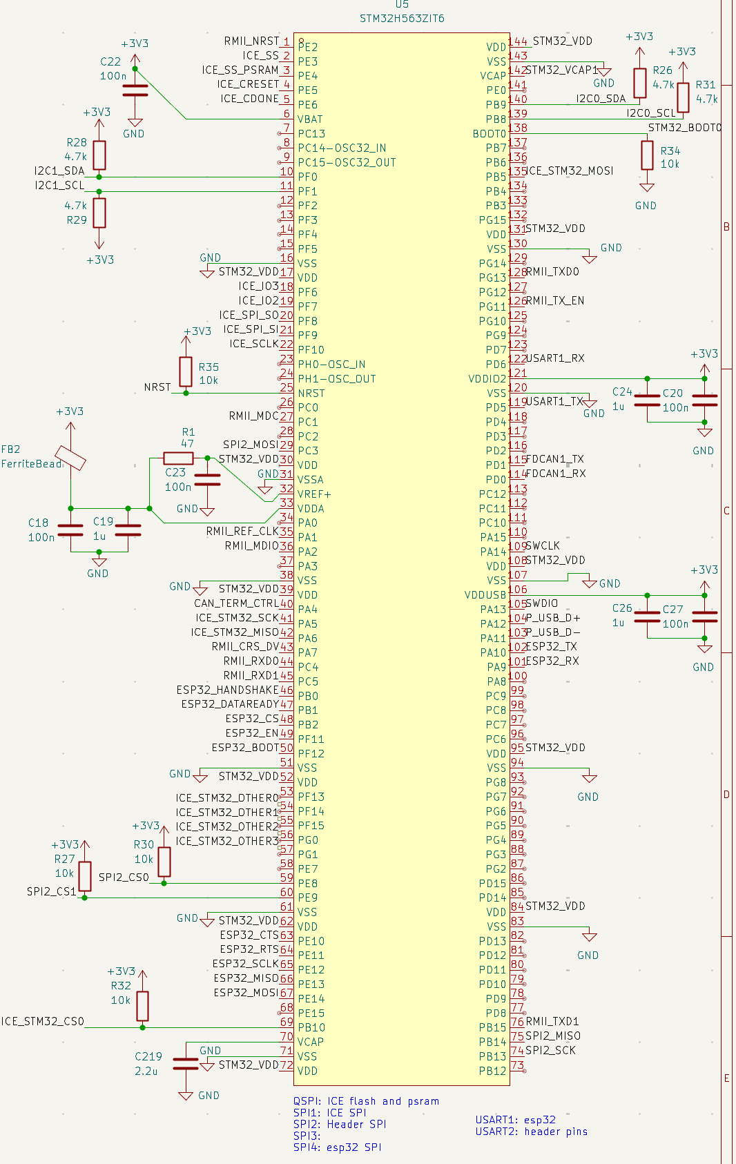
- Started with STM32H563VIT6 (100-pin version), but couldn't get RMII wired properly, so had to switch to STM32H563ZIT6 (144 pins). That's going to be interesting when I start tracing
- STM32 is really needed instead of the RP2350B, I need plenty more SPI connections: 1. STM32 to the PSRAM (shared with ICE40 for the buffer), and also shared with the flash so STM32 can flash the ICE40. 2. SPI between ICE40 and the STM32. 3. SPI between ESP32 and STM32 for faster WiFi. AT is a bit slow, so I'm thinking of going the esp32-hosted-mcu route. Still have UART wired with RTS and CTS in case we need to do AT, and we want to have a bit more bandwidth 4. SPI to headers to proxy flashing of the ICE40 if needed
- I2C count stayed the same, but the combination of SPI+QSPI+RMII looks like I'll not have that many pins left on the 144 pin version either (still plenty though)
- The ICE40 has a separate VCCIO, so we can make the Logic Analyzer pin voltage configurable
- RMII needs lots of pins
- The STM32H563 also supports CAN, so that's where the CAN will be controlled from. The termination is now also behind a switch, so we can control termination in the firmware
- Lots of BOM constraints if we want to keep the board inexpensive to manufacture. Analog ICs are the most expensive. Switched some expensive old parts for their newer counterparts to save a bit
- Also, analog requires a wide range of voltages. Might switch over to a dynamic LDO and see if that is less expensive than having lots of different ones (it will be for low volume for sure, with the loading fees)
- Wiring ethernet was pretty straightforward, following the nucleo reference board for that
- Also realized that even with 144 pins, it's worthwile considering GPIO expanders so I don't have to wire all these single wires all over the board and instead connect to the I2C bus that is close by anyway
- Also, STM32H563 is surprisingly inexpensive at around 6-7 USD depending on pin-count. The benefit of having RP2350B quickly disapears (the RP2350B has a few external parts that you have to take into account also, and it has no ethernet support, so you'd need a more expensive ethernet component)
Below the 144 pins. Lots of free space still, but the SPI/I2C/UART pins obviously can't go on any pin, so it's more tight than you'd expect:
![]()
-
Python pytest package
06/10/2026 at 15:49 • 0 commentsThe pytest library is available on PyPI: https://pypi.org/project/embeddedci/. You can now run the hardware tests directly with pytest using pip install embeddedci and the pytest command. Now I'm going to finish up testing v1 and start making the changes needed for v2, which should be a board that actually should be able to go through the full flow:
- Attach BenchPod to a target device
- Configure WiFi/network and find the device on the network (using our CLI)
- pip install embeddedci
- run pytest
- integrate with GitHub actions (local runner or using our EmbeddedCI.com cloud to "proxy" the requests)
-
More bring-up work
06/09/2026 at 14:32 • 0 commentsA few things I've been doing since the last project log:
- Writing firmware to test all components
- Decided not to use PIO after all, the MCU will only orchestrate, the dataplane will be the iCE40 (FPGA)
- When not using PIO, there's no need for the RP2350B anymore; most likely, I will switch to STM32H563VIT6 so that I have MAC support. It's actually less expensive to use the STM32 without an external flash, oscillator, inductor, or MAC chip. It’s actually close price-wise, but the RP2350B is short on SPIs if you need Ethernet. Too bad, because I liked the dual-core (didn’t use it yet, though) and PIO (FPGA replaced PIO for my use case).
- Did lots of FPGA test cases. The iCE40 is really nice to work with when it suits your use case.
- Didn’t have much time to test the analog path yet, but spend instead a lot of time on v2, which will have a calibration path (DAC to ADC), higher precision (14 or 16 bits), and higher voltage support (the ADC will have a 12:1 attenuator, so we can take -+ 30V in and DAC will be have a 3V3, 5V and +-12V path)
- Also had to use a heat station to put the ESP32 in place, as JLC didn’t put it (the component would put me out of PCB Assembly economy, so I opted to do it myself after the board was validated enough). I was hoping for castellations on the chip, but I took the version with pads unknowingly at the bottom instead of on the side. It’s a bit trickier, and although the ESP32 gets its voltage, I can’t reach it over UART/USB. I’m also missing a pull-up on a pin, but most likely I'm accidentally shorting the EN port (that's what the continuity test shows), and it needs a reflow.
- Working now on some pytest cases to flash a target device, use eFuses to manage power, check UART, launch sensor simulation over i2c, enable on-board pull-ups, and see if the firmware of the target device can see the sensor. The UART, I2C, and SWD are all done in the FPGA with the iCE40. Here’s a snippet of the Python test code:
# Flash → emulate BMP280 → power cycle → assert UART in one test

import re
import pytest
from embeddedci import benchpod as bp

APP_OK  = re.compile(r"APP_OK")
PRESENT = re.compile(r"chip id match=0x58|bmp280_detected=yes")


@pytest.mark.hardware
def test_bmp280_sensor_present(benchpod, pins, firmware):
    """Flash DUT, emulate BMP280 on I2C, power cycle, assert on UART."""

    # 1. Flash
    result = benchpod.flash(
        file=firmware,
        target="target/stm32f4x.cfg",
        swclk=pins.swclk, swdio=pins.swdio,
        nreset=pins.nreset, target_power=pins.efuse,
        verify=False,
    )
    assert result.ok

    # 2. Emulate BMP280 on I2C
    #    I2C is open-drain; enable pull-ups so the bus idles high.
    benchpod.enable_pullup(pins.i2c_sda, pins.i2c_scl)
    benchpod.enable_i2c_sensor(
        bp.Sensor.BMP280,
        sda=pins.i2c_sda, scl=pins.i2c_scl,
        address=bp.BMP280_ADDR_PRIMARY,
        temperature_c=22.5, pressure_pa=101000,
    )

    # 3. Power cycle + capture UART
    cap = benchpod.power_cycle_and_capture(
        rx=pins.uart_rx, tx=pins.uart_tx, efuse=pins.efuse,
        delay=1.5, duration=6.0, until=PRESENT,
    )

    # 4. Assert
    assert cap.match(APP_OK),   f"no APP_OK banner:\n{cap.text}"
    assert cap.match(PRESENT), f"BMP280 not detected:\n{cap.text}"
    assert benchpod.i2c_sensor_status().get("transactions", 0) > 0
Here's the test running:
![]()
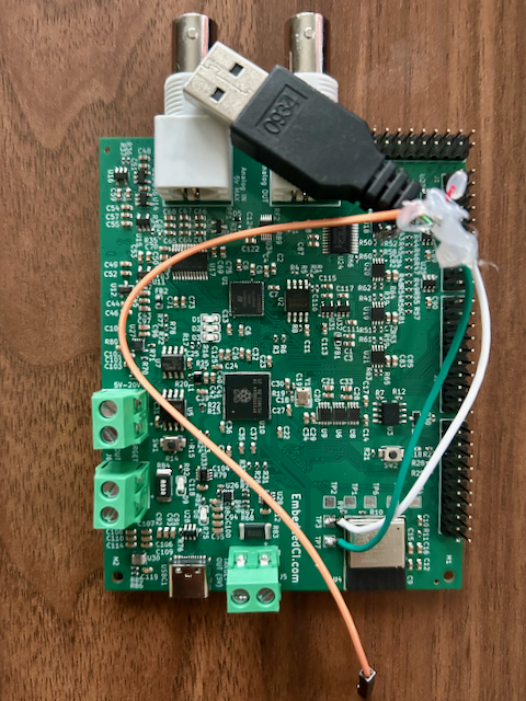
Also, here’s a picture of the ESP32 test pads with the USB data ports. Connected it to a USB cable to see if I could see anything, but as said earlier, it’s most likely a reflow issue. Still, I found it interesting that you can just solder a USB cable to the data ports.
![]()
-
Bring-up time!
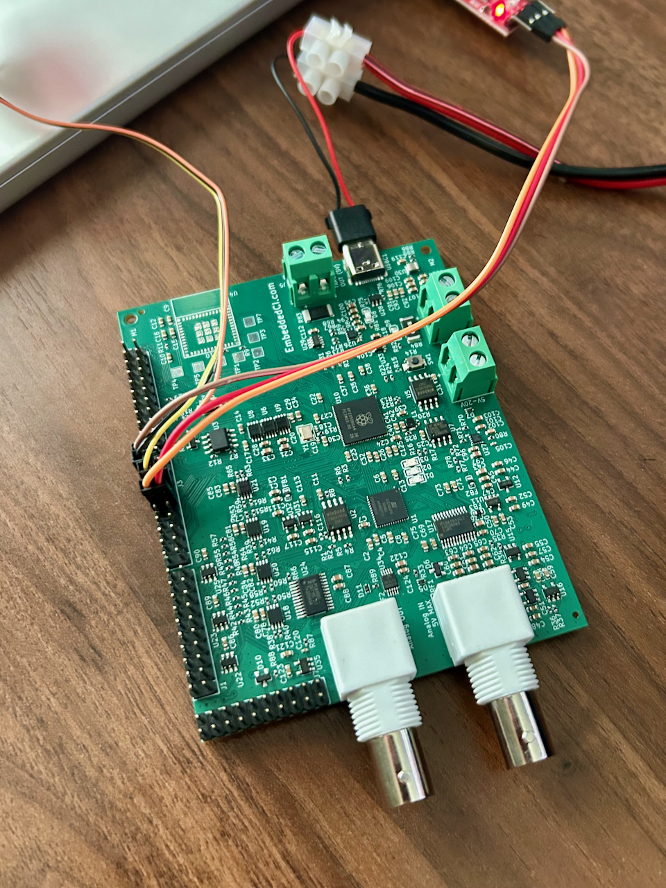
06/04/2026 at 16:57 • 0 commentsBring-up went well; so far, everything except one minor issue: the RP2350B's flash. Here's a picture of the board, then more about the W25Q64JVSSIQ (flash) component.
![]()
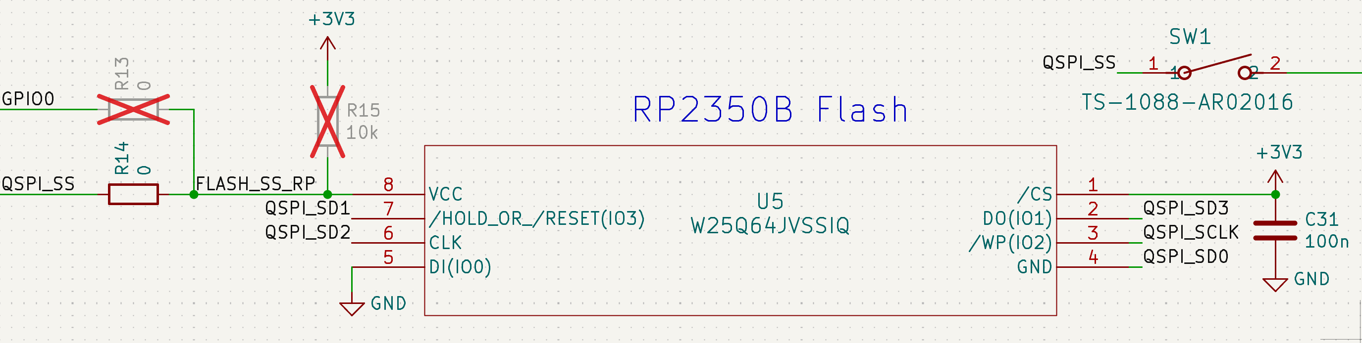
While doing the PCB layout in KiCad across 2 screens, with the mouse pointer focused on the schematic view rather than the PCB window, I accidentally hit a button, and the flash component moved within the schematic. I only realized it a few minutes later, so I couldn't use ctrl+z. I moved the flash symbol back, fixed the messed-up wiring, and continued with the PCB. What actually happened that I didn't realize is that the symbol was mirrored, and all the wiring was correctly placed, but to the wrong, mirrored pins. I then traced it like that in the PCB, and that's how my flash doesn't work in v1. Luckily, I don't need it, so I just flash to SRAM instead for this version. The flash for the iCE40 was actually untouched, so that one works! Here's a screenshot of how the mirrored symbol looked, pretty obvious, but I didn't check it in detail in the schematic anymore, as I didn't make any changes.
![]()
-
Prototyping and LTspice
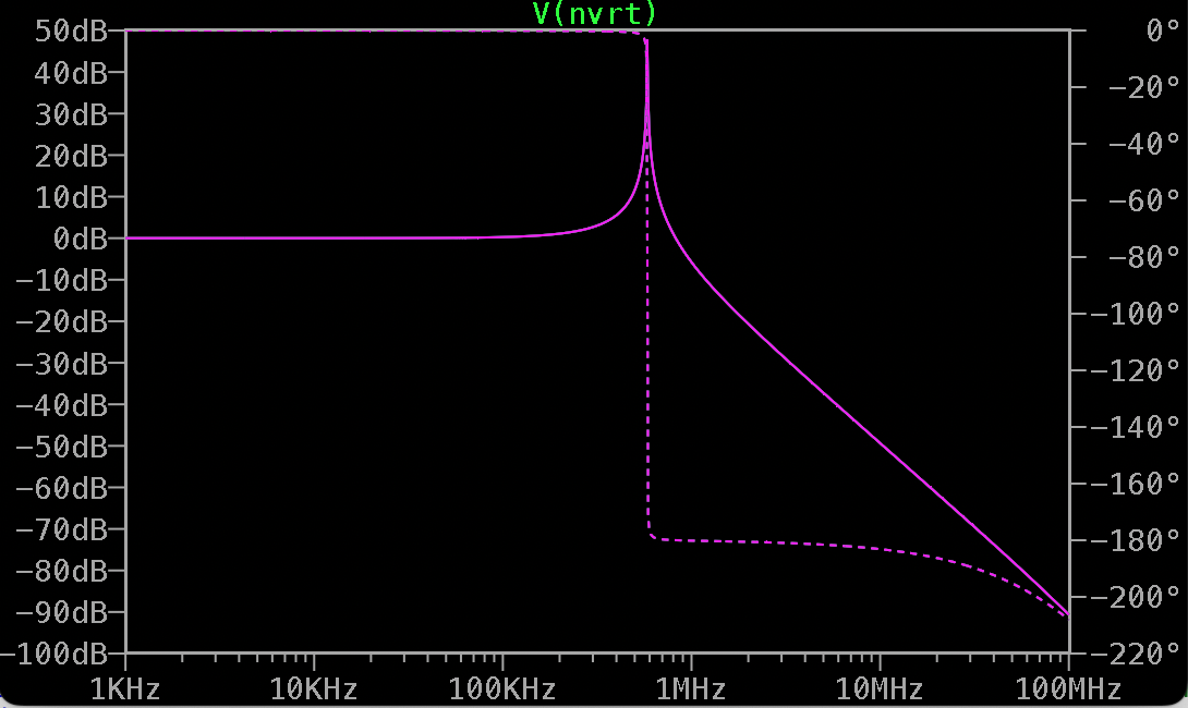
06/03/2026 at 14:28 • 0 commentsQuickly shipped the v1 of our bench board to validate bring-up while still iterating on the design. Did I know analog has such a steep learning curve?! Finally sat down to do a full SPICE analysis and... turns out I've been feeding pure noise straight into my ADC. The VTOP and VBOTTOM pins of the ADC08060 are missing their resistors. Oopsie. Guess I'll be scratching a trace or two and squeezing in some resistors.
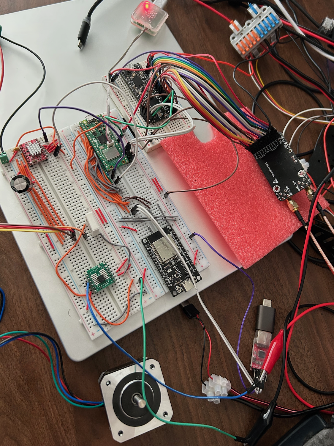
Also tried to replicate the analog capture flow using a cheap Aliexpress ADC/DAC and a step motor, only to realize the ADC does AC coupling, and my DC signal is gone. Definitely spending some more time than anticipated on the analog path for the waveform capture, replay, and fault injection.
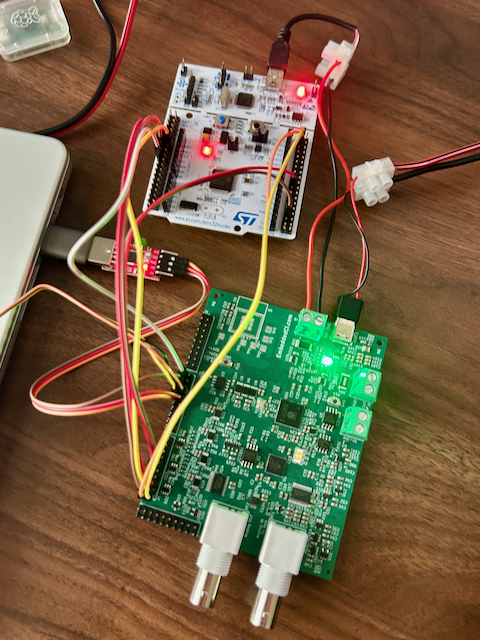
On the pictures:
1) breadboarded the iCE40 + RP2350 + ESP32 (wifi) with the iCE40 connected to Aliexpress ADC/DAC (DAC works end-to-end over wifi, but needs another ADC for capture to work - the v1 that will arrive shortly with the noise issue, but that's solvable)
2) LTspice showing the missing resistors on the ADC input pin![]()
![]()
-
Why BenchPod and Why It's Built This Way
06/02/2026 at 21:24 • 0 commentsLet's talk about BenchPod's design decisions. The first version is produced by JLCPCB and is in transit. Once arrived, I'll test the basic functionalities and iterate on the design.
The core problem that BenchPod is built around is that test hardware doesn't scale across a team. A board sits on one engineer's desk, someone else needs it, and people end up waiting or working in the dark. Using a board usually means being in the same room as it is. Flashing firmware, running tests, checking a signal, none of that should require physical presence. So the design goal for v1 was a single board that lives in the lab and that the whole team can reach remotely. The goal is also to not make it too expensive, so you can keep the board attached to every target.
Why RP2350B
The RP2350B is the 80-pin variant, chosen for the extra GPIO since this board has a lot to drive. It also has PIO, which can run protocol logic in dedicated state machines without tying up the main cores. That covers many peripheral mocking use cases without requiring anything more exotic. RP2350B will handle most of the digital stuff (I2C & SPI sensor simulation for example).
Why an FPGA
For everything PIO can't handle, faster protocols, the logic analyzer, analog input capture, there's an iCE40 on board. It's an inexpensive way to get real FPGA capability without the board cost getting out of hand. In v1, the FPGA is handling logic analysis and analog input.
Power control
Being able to turn the target board on and off remotely is more useful than it sounds. It means you can flash a new firmware version, power cycle the board, and watch the serial output without touching anything. That makes BenchPod a natural fit for a testing pipeline: flash, boot, test, repeat. You could also keep devices powered off until you need them, something that might be useful if you have lots of them.
WiFi and the ESP32
The decision to have a separate chip for WiFi rather than a combined solution was deliberate. Keeping connectivity separate from the main MCU means the RP2350B can focus entirely on the testing workload. The ESP32-C3-MINI-1 was the practical choice: it's pre-certified, JLCPCB can assemble it, it's inexpensive, and there's official AT firmware that handles WiFi over UART. A Pico 2 W would have worked too, but it costs more and doesn't have out-of-the-box AT. I might revisit this choice when adding Ethernet, though, or if I find a decent, inexpensive ESP32 alternative to use as a WiFi modem (the alternatives are quite expensive, so I settled on this).
On the analog side
The analog input is the most experimental part of this design. The current setup is basic, 8-bit, and limited bandwidth. The goal for v1 is to validate the signal path and the architecture. If that works, bumping up the resolution and speed is a straightforward next step. I've already started designing v2 analog input/output, and one of the differences is going to be supporting higher voltages, then scaling them down, so we keep the precision.
CAN
CAN support is on the board for when it's needed. The idea is to simulate devices on a CAN bus, which is useful for teams building anything that talks CAN. The details of how that gets exposed in the SDK are still to be worked out.
What v1 actually is
This is a bring-up board. The goal is to find out what works, what doesn't, and what needs a respin. It's not production-ready and isn't trying to be. The schematic and PCB were sent to JLCPCB last week and the boards are now in transit, with delivery expected soon.
Board Layers
4 layers. Most important signals on the top, then 2 GND layers, then the signals that don't fit on top + power. After watching Rick Hartley's lecture explaining proper grounding, I ended up with 2 solid GND planes to ensure signal integrity for the analog part ([1] YouTube link at the bottom).
The KiCad files are in the GitHub repo. Here's a view of the PCB:
![]()
[1] Proper grounding:
BenchPod
An open hardware bench tool that plugs into your CI: sensor sim, CAN, analog I/O, power control, and a Python SDK with pytest integration