HQ Wireless Audio
I don't want to pay $200, when i can pay $250 and learn something. Wireless audio by someone who doesn't know anything about it.
I don't want to pay $200, when i can pay $250 and learn something. Wireless audio by someone who doesn't know anything about it.
To make the experience fit your profile, pick a username and tell us what interests you.
We found and based on your interests.
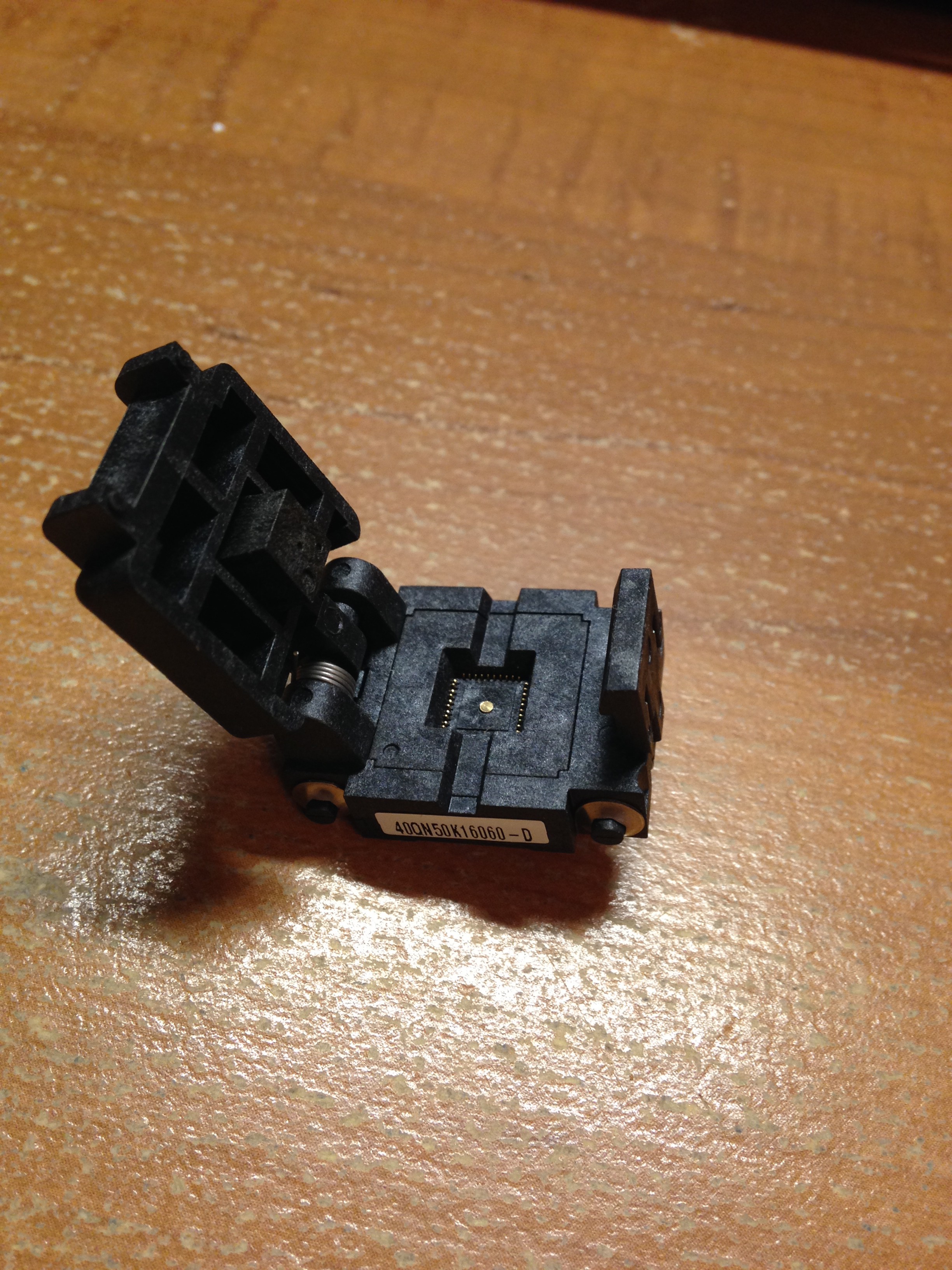
Socket showed up, looks awesome. Long pins on the bottom, I could probably get away with a spring hook connection to the required pins, but I think it should be simple enough to modify one of the many qfn breakout board designs to accept a socket instead of a chip directly, and then I can stick it in a breadboard. Open socket pics below:
From Above:
The Bottom:
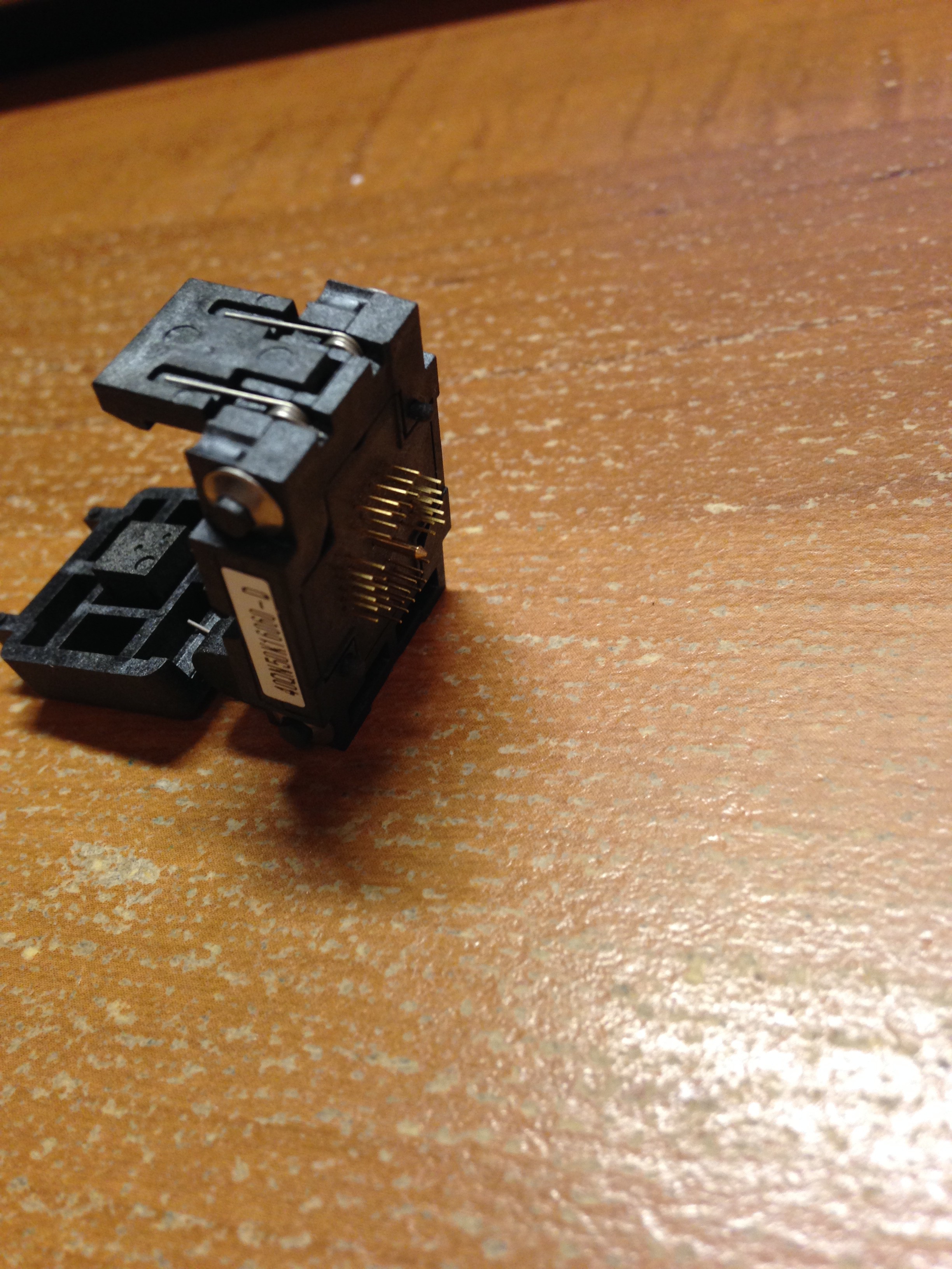
The pics make it look big.
I know it has been a while, but I believe I may be able to move forward with this project again soon. I found a socket for the QFN40 package that wasn't $80+. When it arrives, I will see how I plan on breaking out a chip to test/program before putting it on a board.
As per my last post, I bodged some thin copper wire as pins onto the ccdebugger header pads, in an attempt to see if the pogo pins were my issue. I have discovered that they are at least not my only issue. Still no love from the purepath wireless configurator software, it doesn't see the chip still. I don't have an oscilloscope to dig deeper, but I have metered the voltage at specific points to determine whether my connector was backwards or something. Next step is a step backwards, removing all the non-comms components from the board, to make sure there are no conflicts there. The only other thing I can think of that may be the issue, is if my reflow didn't take everywhere, but I can't think of a way to test that. Ideas are welcome. If the component removal doesn't do the trick, I will have to make a breakout board for just the wireless chip, and attempt to get comms going with it.
Hey all - Sorry I haven't moved forward with the project. Got another stuck in my craw, with the ESP8266.
I have a question for you fine folks - I was wondering about the possibility that my problem with communicating isn't with my board layout, but rather with the connection. I believe i mentioned in a previous post that I have stuck some pogo pins in the end of the female connector on the ribbon cable from the CCDebugger, and it has recently occurred to me that my failure point may be the point - of the pogo pins. They are a spear tip design (this product) with a tiny point. The picture at the link doesn't do them justice, you have to visualize the dimensions shown. That single point of contact is tiny. Easily smaller than any of the trace widths on the board, possibly even smaller than the pads on the IC's.
Could I have a power choke at that connection? I may kludge on some sort of header and try to fire it up again before de-soldering everything.
Thanks for any input!
I have populated the board, reflowed using a toaster oven. It worked well, as far as the reflow process went. unfortunately, there are no blinking lights and no communications with the programmer. I am now working on troubleshooting the circut. If I don't get anywhere doing that, I will probably mount the CC8520 chip on a breakout board and test it that way, before attempting another full blown transmitter. I will probably also attempt to remove the chip with the hot air process as well.
Boards showed up. What immediately struck me is the bare metal at the antenna connection points. I didn't think to remove it from the solder mask, as they aren't really pads, just connections on the signal plane.
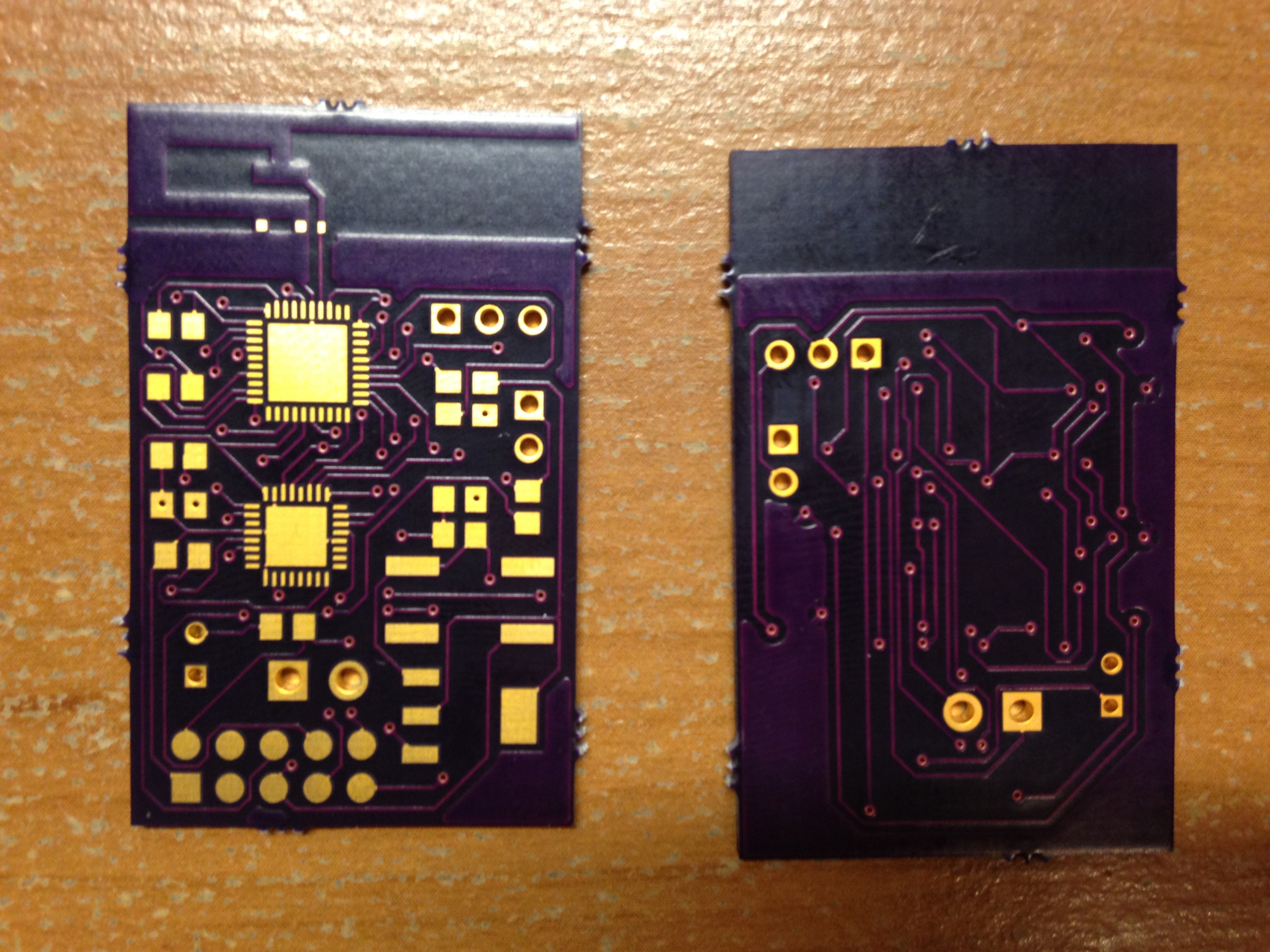
Boards are slated to arrive on Saturday, 1.17, and with a holiday weekend, I imagine I will be able to find out if my design at least communicates with the programmer. I have the Master/Sink board designed (it was a very small change from the Slave/Source board), but I believe it prudent to put my hands on the first board and get a feel for how it came out before I submit the next set to OshPark.
I woke up last night, concerned that the programming pads were incorrectly oriented on the board, but my concerns were invalid. A check this morning confirmed that all was well.
I did notice that the current configuration is for a Slave/Source. Slave units are better suited to be the battery operated end, so it looks like I will be creating the wireless guitar pack first instead of the headphones. Not a huge issue, but not what I had intended on creating first. I should have created a Master/Source unit, or a Slave/Sink unit. Next will be the Master/Sink unit, to complete what is now the guitar pack.
I have adjusted components to what I plan on using, and have re-done the PCB. It is pretty small, 26x42mm. My first unit is intended to replace a cable from my monitor station to my in-ear monitor on stage, so plug in location is not a huge issue, but if the unit operates well enough, I will probably re-design the PCB layout again, with the intention of running a 1/4" jack out the center of the back, for the purpose of plugging into my guitar, to keep it tight to the guitar body. This particular piece is getting a 1/8" jack for headphones, and it may be just a whip out of it, I haven't decided yet. PCB screencap below, as well as the download links for the schematic and pcb for diptrace. As before, the DRC error circles are all related to the antenna. Next step is to have it printed out and attempt a toner transfer method with it. All those vias worry me though, I might not have a choice but to have it done from a board house. Scratch that, I submitted it to Oshpark just to see what the price was, and I can't argue with $8.50 for 3 boards, including delivery, so I now have boards en route.
First draft of the schematic and board (just to get an idea of how small I can go, and to attempt to work out the details regarding the PCB antenna.
Schematic first run:
PCB first run:
All done in Diptrace. The DRC error circles are all related to the antenna, it is a part created of shapes on the signal plane, using the dimensions for the TI inverted F antenna. I couldn't figure out how to make it see all the shapes as one piece, either in the part creator or the PCB layout, so if anyone has any tips regarding that, I would happily utilize them. I know that it is missing some passive components yet and a couple of the parts on there are just placeholders for the moment, so the next step is fine tuning the schematic, adding all the passives and replacing parts with the ones I intend on using. I will probably completely re-do the PCB layout as well, I think it can be smaller. Currently it comes in at about 43.5mm x 29.5mm. I will likely make it the width of the antenna, and drop everything under that. They aren't labeled on this layout, but U1 is the CC8502 wireless chip, and U2 is the codec.
I have also gone through all options for the programming of the unit, the PurePath Wireless Programmer software from TI is really easy to use, it limits all options based on which chip you select, and what role you want it to play. Many of the options in the software affect what pins you use, so it was a good thing I was thorough.
Create an account to leave a comment. Already have an account? Log In.
Curious... if you've considered using nRF24L01(+) radios?
Hello zacnotes! I am starting to develop a project similar to yours and I was interested on knowing if you ever managed to overcome the problems you found.
Regards,
David
Hi, I have built 2 radio mics ( body packs ) with CC8530 / PA module and AIC3104 and a reciever with AIC3101 with a module and Codec on a protoboard. I ordered the TI Codec from proto advantage in Canada which made life easier ! how anyone can solder these things I have no idea..
I would say though that you should use seperate power supplys and keep analouge & digital GND & power sperate as in the data sheet or things get really noisey ! Also dont bother using the AIC3101 mic bias power if your powering an electret mic ( use your own supply from battery ) as the CC85xx makes a nasty audioable RFI at around 300-400hz, documented in the TI forum. The range at full power with the PA is'nt that great for me and you get dropouts when the mic moves about. I used the diversity option and assighned the mic as diversity Slave and reciever as master. you will need the CCdebugger to program the cc85xx. its quite easy to program with the ti's configurator software and you can add some register settings for the AIC310x if you want. anyway, if you do get to build this and you want any info just let me know.. not sure I can help but you never know !! I used pre-made CC8530 modules from Raytac ( Taiwan) already built with the PA with UFL connector since the range is ussless without the power amp( maybe 10 meters ). CC85xx and PA need to be built on 4 layer board I think to work properly.. Although I did add the Switchcraft diversity switch after a UFL connector on module output for diversity switching. there is a TI example design of that. I would say if you add the skyworks switch for diversity antenna then shield that area., maybe that helps with rf loss around the switch.. I used the proper capacitors ( 50v 5%) as in the TI example but I think you could get away with any !
also, just an idea, but I found I needed power on the CC8530 and not just from the CCdebugger to program or see the device in the configurator... could that be your problem? I was also tempted by the adapter socket but at 85$ I thought i'd give it a miss !! I also just soldered some 0.5mm DAC 48 pin to a prototype board and it was'nt as difficult as I thought it would be.. although I have'nt wired that up yet so we will see if it works !!!
I haven't tried with power supplied outside of the debugger, I will have to give that a go. Makes me at least mildly hopeful that my initial board design isn't a complete failure. I will let you know how it goes.
The socket was a great find, I have regularly checked a number of locations for a socket that didn't cost more than I have spent on the whole project, and was cautiously hopeful when I found this one on ebay. I suppose there is a pretty small market for people trying to buy a temp socket for a qfn40 package; i was the only bidder.
did you manage to program the CC8530 with the supply power added ?
theres some video of 2x CC8530 module mics working on my page in the arduino audio midi mixer project description in case your interested.. the video demonstrates the horrible RF noice at arround 300khz pretty well.. i did manage to get rid of this noise with a filter at some point but forget how I did it.. anyway, I'm moving on to UHF radio mic design with a PLL. will let you know if that gets anywhere !
anybody who has the huevos to solder wires to such a small chip has my interest. i was looking at doing this to some Silicon Labs hardware, and i thought better of it. ti (and formerly Burr-Brown) has excellent audio intellectual property/hardware - so does Wolfson.
hi zcnotes . i working at TI aic3254 and pps software i looking for TIDM-WIRELESS-MICROPHONE : http://www.ti.com/tool/TIDM-WIRELESS-MICROPHONE?keyMatch=cc8531%20dongle&tisearch=Search-EN-Everything
I have been wanting to play with the PurePath chips for months for an in-ear monitor project. I'm disappointed that they're only available in UTQFN, and it takes three ICs (the transciever, the converters, and the "range extender" to put it together. In fact I'd be happy with an analog transciever that works in an ISM band like 900MHz, but they apparently don't exist anymore. It's cheap iPod FM transmitters or nothing. Also if you want to effortlessly solder those QFNs plus the ground pad (which needs to be connected for it to work), check out these: http://www.schmartboard.com/index.asp?page=products_smttodip&id=633
No new developments, I haven't touched it for awhile. The project gained a couple of new followers, so I am feeling a bit guilty about the lack of progress. I have a bit of time off from work here over the next few days, with no real obligations, so I will attempt to go a bit further. Also see the new post.
No pressure :) I just found your project and like the idea.. I think most of us know what it's like to have other (important) work to do as well ;)
Become a member to follow this project and never miss any updates
By using our website and services, you expressly agree to the placement of our performance, functionality, and advertising cookies. Learn More
 Josh Kittle
 Mike Teachman
 Ken Yap
 Nathaniel
Love this amazing personality. I'm also making the project on Celebrity of Maya Moore, you can read more about it here https://networthsize.com/maya-moore-net-worth/