Yann Guidon / YGDES
-
Making Y8 more energy-efficient with a deglitcher
03/30/2019 at 18:54 • 0 commentsWhen you create you processor, you want it to work, then priorities shift to speed because the processor must be compared on its merits. Then... it's over, it's too late, the infernal bikeshedding machine is in motion and hard to steer.
One thing is sure, however : the industry has spent the last 15 years steering toward energy-efficiency, toward more MIPS per Watt and it's often overlooked in the early drafts for amateur designs. We don't care how much our pet machine will consume, since it won't run that long or that much. But efficiency is a staggering goal, even more than performance because today we have so much power at our fingertips. But think about this : if your processor runs 2× slower but uses 3× less energy, you are actually winning and you can put 2 or 3 processors in parallel easily.
Energy efficiency is not a significant goal for the #YGREC8, nor is performance, or else I wouldn't bother with a relay version. I don't expect the ASIC or FPGA version to run on a battery but you never know. It's never too early to build this into a design that is intended to be the basis for larger designs... And those designs will want to avoid using a heatsink.
Today, CMOS is the dominant technology and the initial target of my designs, either in FPGA or ASIC (the rest is for the lulz). Its consumption is proportional to three main parameters C-T-V :
- power supply Voltage (squared) : reducing the voltage is a simple and easy way to reduce the power, to a certain extent at least, because the out-of-range values will not allow the circuit to run fast (or at all).
- Capacitance : the gates of the transistors act like capacitors that must be charged and discharged. The capacitance drops as technologies shrink, which we can't control easily, but as a rule of thumb: the more transistors are toggled, the more they will consume. That's an interesting angle of attack...
- Toggles : the faster you run the circuit, the more charges and discharges, the more energy is needed to switch the transistors. Energy-saving methods often include running the circuits slower.
Some of those parameters are in the realm of the implementer. For example, the supply voltage or the frequency will not directly affect the logic of the circuit (within the nominal operating conditions of course).
Some other parameters are directly under the control of the designer, and can be summarised as : toggle less, less often.
I have mentioned running the circuits slower, but there are other methods as well, some belong to the purely digital design real, others on silicon sorcery, such as playing with a voltage bias with the bulk of the substrate, altering the temperature, changing the doping or composition... Let's forget them.
What matters at this level is what we can do at the architectural level. We can't control the clock speed in the absolute, but any design choice affects either latency/speed or consumption, usually both. And this is relative.
One textbook example is "clock gating" : drive the clock input of the group of DFF that really need to be updated. It's easy to do, and easy to mess up, because it's at the edge of timing analysis and FPGA prefer "clock enable" with one main clock.
Clock gating is finely tuned in very low-power devices. Years ago, I heard of a complex processor being split into more than a hundred of clock domains and I'm sure the numbers are much higher today with Intel's latest processors, where not only clocks, but power domains are fine grained. But this technique is not easily portable.
The YGREC8 has other places where some "toggle optimisation" can be effective and easier to design, given the proper framework and structures. One such example appears in the ALU where several control signals not only have to be propagated to 8 (or more) logic gates (a fanout of 8 is not negligible) but the results of the changes will propagate through the rest of the datapath and logic gates. Some bits might not change, some could toggle back and forth during the cascade through the adder... Any change at the input or the control signals of the adder can create an avalanche of short spikes that will consume power.
The truth table of the ALU control signals (processed in the decoding unit) has many "don't care" states, which are currently used to save latency through logic minimisation. These "don't care" states could instead behave as "don't change" in an alternative version of the decoding unit. It's just a matter to keep the propagation time short and the logic simple.
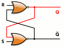
As previously discussed, using DFF or transparent latches would not work, because of timing analysis and increased latency. Fortunately, these are not the only types of FlipFlops and the solution might be even simpler than that :
![]()
The SR latch has one gate of propagation time and the synthesiser will only complain about looping back the output (you can nicely tell it to ignore the situation with some pragmas).
The S and R inputs will be driven by different/separate combinatorial circuits that will only change the output when really required. The remaining input combinations will leave the output unchanged. This can be written in VHDL with code like this:
signal <= '1' when (condition1 OR contition2)    -- SET
     else '0' when (condition3 OR condition4);   -- RESET
     -- no final "else" value !
The synthesizer will not be very happy and will try to generate weird stuff. It needs "some help" to swallow the pill and good coding practice will lay out each equation for SET and RESET, then input them in a custom SR latch, using a lower level description.
In the case of the A3P family (and probably others), there is an extra bonus that uses only one gate/tile instead of 2 NORs :
![]()
This is the OA1B gate looped back to itself. The SET action will be a little bit faster than when using 2 separate gates.
The decoding logic will certainly have more depth than the "optimised for speed" decoder but the decrease in electric activity is worth the slight delay. The fun part is that the SR latch method is retro-compatible with the optimised version and there is no added constraint (no need for more inputs for example). The two versions are easily interchangeable and could even be switched from one to another on the fly for a "turbo" mode...
For a useful example, let's have a look at the boolean map of the ALU in the log ROP2 reloaded:
Opcode F Pass NEG OR/XOR ROP2
muxAND 0000 0 0 × 0 OR 0001 × 0 1 1 XOR 0010 × 0 0 1 ANDN 0011 0 1 × 0 CMPU 0100 × 1 0 × CMPS 0101 × 1 0 × SUB 0110 × 1 0 × ADD 0111 × 0 0 × SET 1000 1 × × 0 The speed-optimised equation for PASS is F3. The toggle-optimised version is
PASS_SET <= F3 and not F2 and not F1 and not F0;
PASS_RESET <= not F3 and not F2 and not (F1 xor F0);
It's quite more verbose and longer but not exceptionally so. More such boolean calculation can be factored with a sort of PAL-like array.
OR/XOR, like the others, takes each result value apart and groups them in the SET and RESET equations:
ORXOR_SET   <= '1' when  OPCPDE=Op_OR else '0';
ORXOR_RESET <= '1' when (OPCPDE=Op_XOR
                      or OPCPDE=Op_CMPU
                      or OPCPDE=Op_CMPS
                      or OPCPDE=SUB
                      or OPCPDE=ADD )
                        else '0';
it's not really complicated when an explicit declaration is used.
ROP2mx can also be rewritten with split SET and RESET equations:
ROPmx_SET <= '1' when (OPCPDE=Op_XOR
                    or OPCPDE=Op_OR )
        else '0';
ROPmx_RESET <=  '1' when (OPCPDE=Op_AND
                       or OPCPDE=Op_ANDN
                       or OPCPDE=Op_SET )
           else '0';
Do you see now how it works ?
Update:To better work, the decoder needs an "instruction enable" latch signal that arrives late enough to prevent glitches inside the decoder itself, but not too late either. It must also be controlled by the FSM because not all outputs from the Instruction Memory are instructions (think LDCx...)
-
A new unit : the decoder
03/29/2019 at 07:03 • 0 commentsI'm starting to update and refine the architecture of the Y8, by making a separate unit, that will hopefully be more flexible.
Uusally, each unit will receive the required parts of the instruction word and decode the necessary signals. This is very easy with a clean RISC processor, which could be described as a "distributed decoding" architecture.
In practice, there are other constraints as well.
- Structure and layout: the decoding gates often "break" the bitslice-like layout
- Management of fanout: some bits from the instruction word might need appropriate decoding and buffering with a global scope
- Sequencing and states: there has to be somewhere to store information about what the processor is doing, for example with the LDCx instructions and the computed writes to PC, which require more than one clock cycle.
- Power consumption reduction: reduce the current by toggling bits only when necessary.
That last argument convinced me about this new unit because optimising toggles requires a global perspective that each individual unit can't have. The current instruction word also needs to be latched for the multi-cycles operations (such as LDCx).
The decoder is a strip of logic gates that propagates bits from the instruction word, parallel to the bitslices, and decodes and spreads control signals in a "fishbone" pattern (perpendicular to the bitslices).
This increases the complexity of the clock and timing because performance dictates that the units must get their respective instruction bits directly from the program memory.
- If the instruction must go through a DFF, the value is delayed by one clock cycle and throughput/execution speed is hit...
- Going through a transparent latch saves time but increases the sensitivity to timing anomalies. A multi-cycles clock becomes necessary.
One solution though is to store the last instruction and combine it with the new instruction with one or two logic layers at most. It might not work for most control signals and it could generate some spikes, which I'm indeed trying to avoid (because they eat power).
I'm also considering adding transparent latches at the data inputs of the ALU.
But before I can add the latches, I have to take the control logic out of the units.
20190330 : I think I've found the trick, using simple RS latches... -
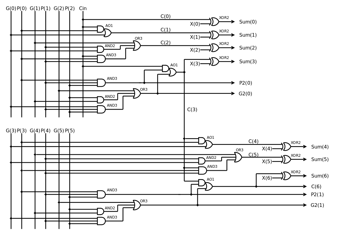
Netlist and structure of the adder
03/27/2019 at 09:07 • 0 commentsThe 8-bit adder has been already covered in the early stages of the design and I found a satisfying diagram/circuit which, though not perfectly perfect, is 95% or so. And it works.
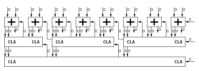
As already mentioned in an early log, I targeted the structure around the Actel ProASIC3 family that uses 3-input tiles. This makes it practical to build Carry Lookahead blocks/units with 3 "bits" of input, and since 3×3=9, it perfectly fits the width of the required 8 bits of data plus the Carry Out flag:
![]()
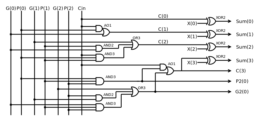
The adder gets the P, G and X inputs from the Logic unit (which is tightly bound). The first bits look like this :
![]()
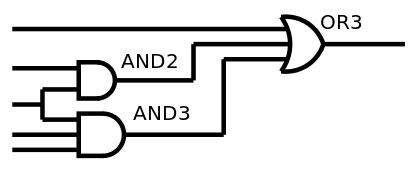
We already notice a recurring circuit made of OR3,AND2,AND3:
![]()
This sub-circuit will be a good target for optimisation at ASIC level for example.
Chaining the first CLA3 with the second one gives the following diagram:
![]()
The logic depth is already 6 gates, not even counting the layer for P and G in the logic unit. There are already 4 "A2A3O3" circuits.
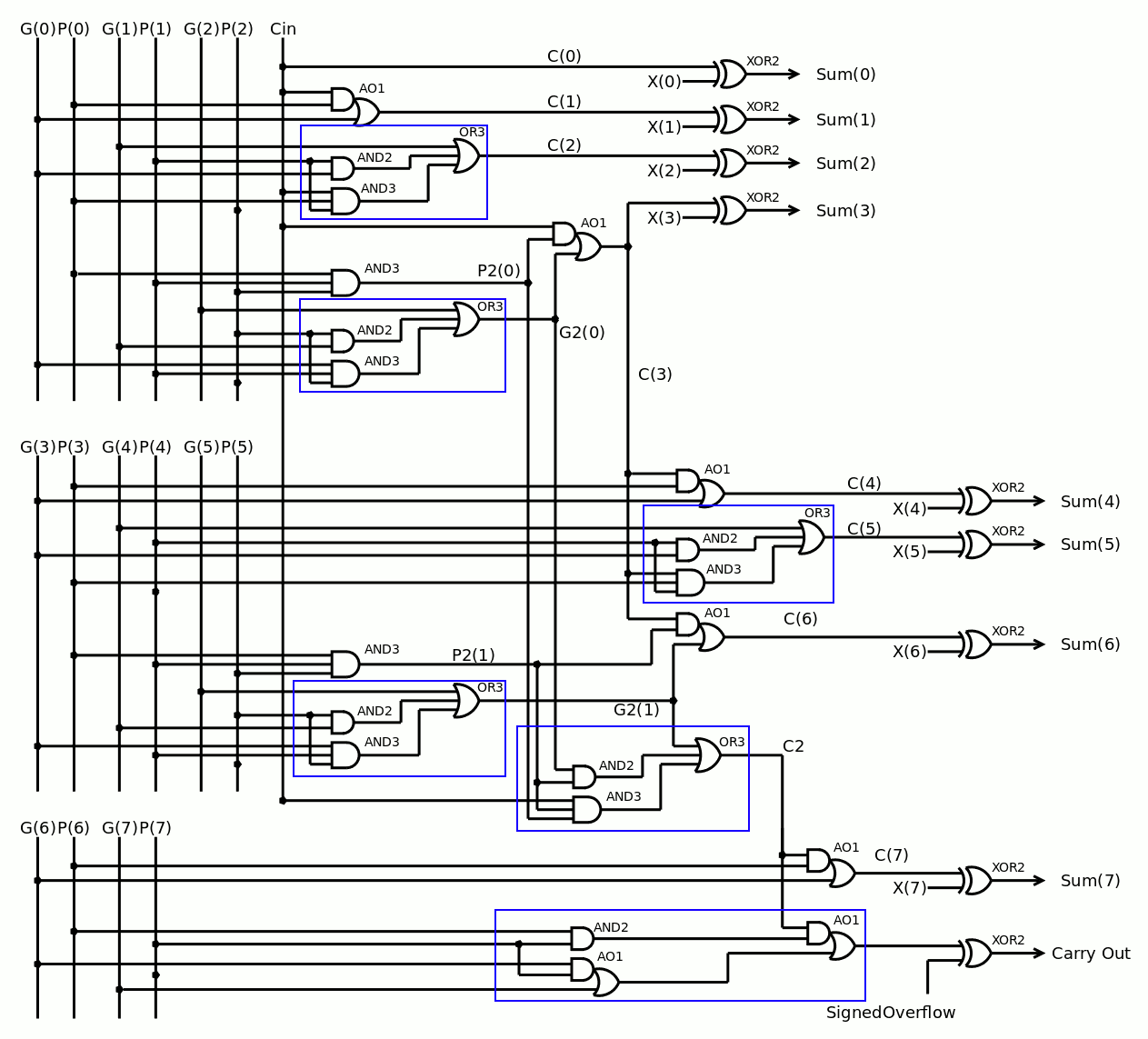
Adding the last bit and the carry out requires some care but doesn't increase the logic depth if some parts of the last A2A3O3 are moved closer to the inputs.
![]()
The fan-in and fanout have been carefully balanced, the maximum is Cin with a fan-in of 5 in the critical datapath. This ensure a reasonable speed for ASIC and FPGA.
There are 25 "tiles" (an average of 3 gates per bit to compute the lookahead) plus 9 XOR, so we must allocate at least 4 tiles per bit for the place&route.
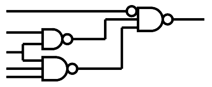
5 instances of A2A3O3 can be pre-routed, leaving 7 other gates to place. These 5 instances can be replaced by the following combo for ASIC:
![]()
-
That ALU should be good
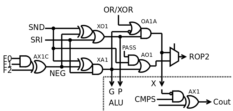
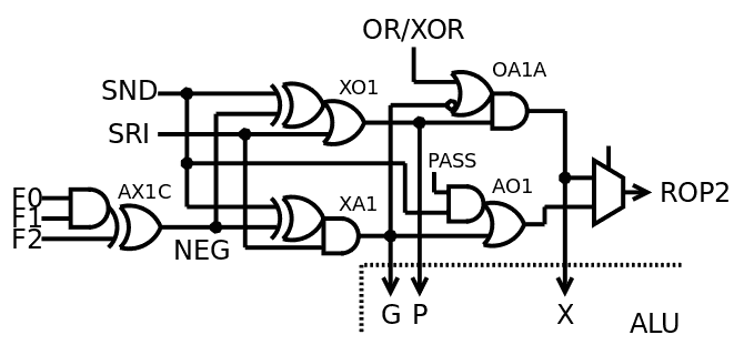
03/25/2019 at 05:47 • 0 commentsI have uploaded YGREC8_VHDL.20190325.tgz that should be the definitive version and definition for the ALU. I must still rewrite the ALU8 with individual tiles but all the rest is good.
I had to find a new trick or approach to implement the signed comparison (CMPS) because the version inherited from the YASEP would XOR the operands, which increases the critical datapath for the MSB and the layout/structure is broken. I saw that the only output bit that CMPS affects (compared to CMPU) is the Carry Out when the operands have opposite signs. My new solution uses the XOR of the sign bits (negated) at the output of the ROP2 section, ANDed with the opcode decoder, the result XORs the carry output bit.
![]()
This new idea is more satisfying because there are fewer gates and the carry bit has a different timing than the rest of the datapath, so it could absorb the additional XOR delay. The ROP2 part is now completely streamlined and homogeneous.
-
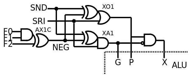
ROP2 reloaded
03/22/2019 at 06:42 • 0 commentsThe log An even better ALU touched a few interesting things but has one fatal flaw : the XOR operation needs the NEGated operand SND, because it is also used by the final stage of the adder! The self-tests don't pass and I now remember why. The optimisation can't be used, but it opens something very interesting...
The following is targeted at the ProASIC3 family but is straight-forward to adapt for ASIC. In particular, the XOR of the SND operand is merged into a 3-inputs "tile" where an ASIC will use a shared XOR gate to drive the first AND or OR gates.
And then, I remembered that the XOR gate can be built from AND and OR gates:

So we can build a circuit where the XOR is the combination of the P and G signals, and an individual (large) XOR gate is not required to be implemented in parallel with them. Indeed the adder needs the XOR at the end of the Carry Lookahead, it is not in the critical datapath and an inverter+AND is not a significant cost.
![]()
From there, you "just need" a pair of MUX2 and you have ROP2 again. Which is pretty alluring. However MUX2 is not a trivial gate in ASIC so there must be a better way to do that, right ? :-)
Indeed (bis) you can do it with an OR gate to force-enable the G signal before it gets ANDed into the X signal. There, you have now 2 output signals that provide AND, OR and XOR. A MUX2 gets this down to 1 signal.
![]()
There is a "free time slot" between the XA1 and MUX2 which can be used to implement the last function : SET/pass. Since it's the output of a AND, it's easy to apply the same idea as before: one of the operands (SRI) can be restored by ORing it back, selectively (though a AND).
![]()
But then, things get, hmmm...
The circuit is great but the control signals require a non-trivial amount of changes.
One consequence is that I have to change the order of the ROP2 opcodes.
The SET/pass feature is in the datapath of AND/ANDN so one of them must be "mirored" with SET. I chose AND as 0000 because ANDN is better left as 0011, to keep NEG's decoding logic simple. This creates the weird situation where OR and XOR are stuck between AND and ANDN, which is solved by decoding F0 xor F1.
Opcode F3 F2 F1 F0 Pass NEG OR/XOR ROP2
muxAND 0 0 0 0 0 0 × 0 OR 0 0 0 1 × 0 1 1 XOR 0 0 1 0 × 0 0 1 ANDN 0 0 1 1 0 1 × 0 CMPU 0 1 0 0 × 1 0 × CMPS 0 1 0 1 × 1 0 × SUB 0 1 1 0 × 1 0 × ADD 0 1 1 1 × 0 0 × SET 1 0 0 0 1 0 × 0 The final equations (some already known) are easy to deduce:
PASS  = F3
NEG = (F0.F1)xor F2
OR/XOR = /(F1 | F2 | F3)
ROP2mux = F0 xor F1
ROP2/ALUmux = F2
And we get the following updated table :
![]()
Time to change some VHDL definitions now...
The assembler is not much affected (autotests passed) because in practice, only AND and OR have been swapped. The ALU code however needs much more work...
For historic references, look at that analysis of a WANG computer._
-
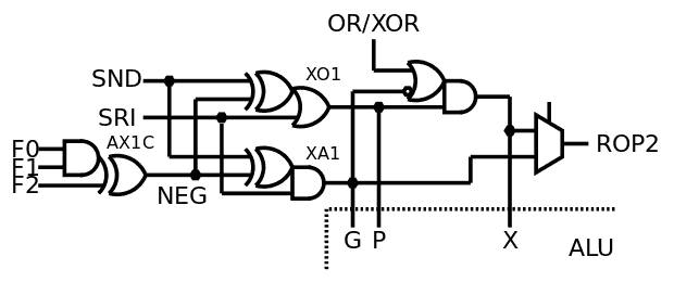
An even better ALU
03/20/2019 at 07:27 • 0 commentsThe log Improved ROP2 explained how the SET/pass function was merged with ROP2. It's a significant improvement but a tiny detail lets us go even further!
Indeed: with YGREC8, there is no XNOR opcode so the source of the XOR gate is not required to go through the inverting XOR of SND. The XOR gate can get its operands directly from SRI and SND, and SND is anded with /F3.
The inverting XOR (for NEG) has now only 2 outputs so this function can be merged with the P&G (OR and AND) gates for the A3P version (at the cost of a higher fanout of NEG, which can be managed through gate duplication). And since the NEG signal has one new "don't care" value, its calculation can be relaxed a bit.
The ROP2 part is now only 5 gates with 3 inputs: 2×MUX2, AX1, XO1, XA1 (of course, this is specific to ProASIC3). This shaves 32 tiles from the FPGA implementation, it's not insignificant...
![]()
There is enough room left for fitting one MUX2 (after the G/AND) but there is no instruction that could use it, since it's too early in the datapath.
Correction : NEG is defined by (F0.F1) xor F2, so it's not MAJ3, but AX1C...
F3 F2 F1 F0 NEG XOR 0 0 0 0 x OR 0 0 0 1 0 AND 0 0 1 0 0 ANDN 0 0 1 1 1 CMPU 0 1 0 0 1 CMPS 0 1 0 1 1 SUB 0 1 1 0 1 ADD 0 1 1 1 0 SET 1 0 0 0 x ![]()
It should work better, now.
AAaaaaaannnnnd.... 57. ROP2 reloaded -
and the new assembler
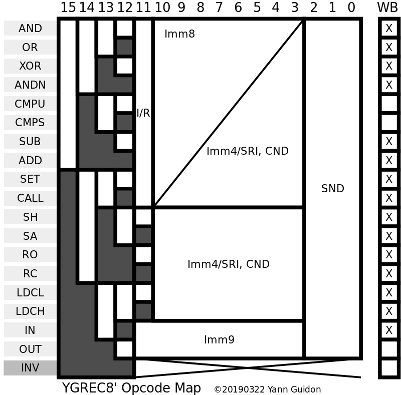
03/17/2019 at 03:06 • 0 commentsThe low-level assembly and disassembly framework is back and running, get it at YGREC8_VHDL.20190317.tgz !
The opcode map has few holes, filtered by ASM_tb.vhdl. The only significant filter is for OVL because the bit 11 is not decoded and there are 256 aliases, that could become an opcode in the future, maybe to control the overlays.
INV is a large chunk of 4096 invalid opcodes, that may or may not be used in the future...
The assembler and disassembler work well, did not significantly change their size or complexity, the code is pretty safe and has only a few quirks.
Yay.
-
The new disassembler
03/14/2019 at 22:37 • 0 commentsToday I finished writing the new disassembler :-)
The assembler will follow, but for now I look at the results and effects of the opcode re-organisation which has broken quite a few things...
The disassembler is deliciously simple and small, with about 100 LOC, thanks to a few well-defined constant tables. Less code means less bugs and corner cases !
I realise that OVL has two encodings because I forgot to take bit 11 into account. There are 2 ways to encode OVL 00h. I don't see the point in adding a 9th address bit. So maybe later an overlay instruction will take a register argument. You never know. But the encoding space is here.
The destination (SND field) is now the last argument in the line, with the optional condition at the very last position. Yes I keep changing syntax rules but this time it fits the instruction format :-)
I have defined 4 opcodes for bit shuffling : SA, SH, RO, RC. These lousy names should and will change in the future...
The assembler will be significantly more complex but I'm confident and I already have the disassembler to cross-test the tools.
-
More high-current germanium diodes
02/11/2019 at 23:43 • 0 commentsI just got a dozen of Д305: these Russian Ge diodes are rated for 10A (50V reverse) with a bulky screwable black-painted body. They were cold-tested at 2.1A (the max of my digital PSU) at 0.38V (two outliers at 0.4V), which is the performance of the OC31 at only 0.5A. They are not cheap, but not very expensive either (for what these are).
The nuts are missing but are claimed to be "metric" and easy to source (M4?). At 2A, and assuming 0.4V drop, the diode would dissipate about 0.8W which should be easy to sustain without extra cooling. For a diode bridge, I suppose I'll make 2 pieces of copper with a few mounting holes (+insulation), as well as a couple of 4mm holes to screw the diodes.
I think we have a winner here :-D
-
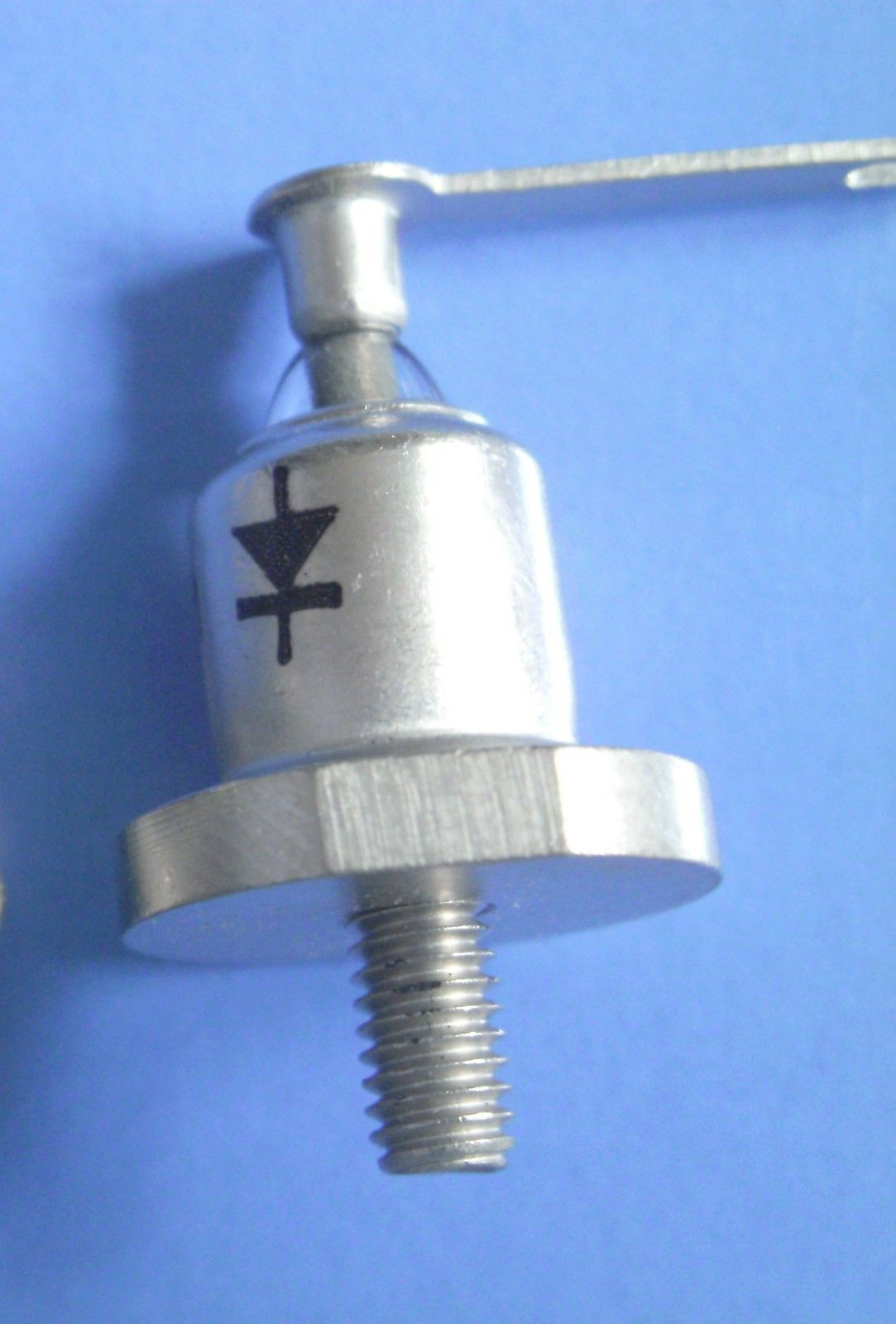
High-current germanium diodes
01/17/2019 at 22:44 • 11 commentsSo far I have only played with nimble, fragile, low-current, point-contact germanium diodes. The "neovintage" power supply of the register set requires higher current than their usual 20 to 40mA rating.
![]()
I got some OA31 from the usual suspect (minifux1) (who provided, among others, essential parts for #Germanium ECL) and they are pretty impressive: rated at 85V reverse voltage, or 3.8A in direct current. Germanium hates the heat (it leaks a lot and the junction should not exceed 85°C usually) so the bulky metal package says we're doing serious business here.
I measured the I/V curve with a crude setup and I'm rather impressed :-)
Direct current (A) Voltage drop (V) 0.05 0.24 0.1 0.29 0.15 0.31 0.2 0.33 0.25 0.35 0.3 0.34 0.35 0.35 0.4 0.36 0.45 0.36 0.5 0.37 0.55 0.38 0.6 0.38 0.7 0.4 0.8 0.4 0.9 0.4 1 0.4 1.2 0.41 1.5 0.43 2 0.45 The curve is quite flat and the drop is lower than silicon diodes and comparable to a good Schottky ! This is a significant progress compared to selenium rectifiers ;-) and the performance for the low-voltage diode bridge will be great :-)
I expect a Vpeak of 4.3V at the output of the transformer (conservative estimate). The diode bridge will "eat" 2×0.45V=0.9V, make this 1V. The diode bridge peak will be at least 3.3V, better than the previous estimate of 2.9V :-)These measurements were done "cold" and are expected to vary with temperature. Not in a bad way, though, because the drop would be slightly reduced. I don't expect the diodes to require a heatsink because they would dissipate an average of 0.5W and they are already pretty bulky.
As previously noted, this could be tested with loads made of many 39 ohms resistors in parallel.
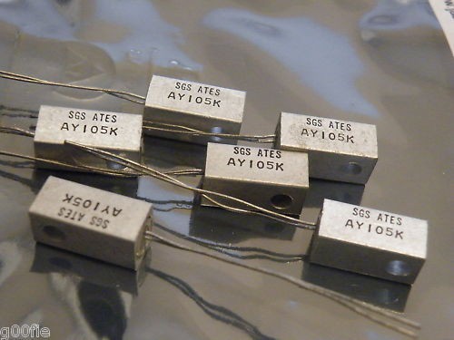
But wait, I also received several AY105K ! They are a little bit smaller and are rated for 5A (a different source claims 3A, which is a convenient margin)
![]()
It's another contender for the diode bridges. Those vintage Italian diodes are smaller and have a more convenient packaging with insulated heat spreader !
However the drop is higher than the OC31 : 0.5V at 1A only, and 0.59V at 1.5A. I would use them for the other power supplies, where the rails are higher voltage (12V ?) and slightly lower current.
I also expect to receive a few Д305 for comparison. They are claimed at 10A so they should be impressive, though I won't have enough to make more than one bridge. So far the OA31 is the clear winner :-)
YGREC8
A byte-wide stripped-down version of the YGREC16 architecture