Yann Guidon / YGDES
-
Another opcode re-organisation
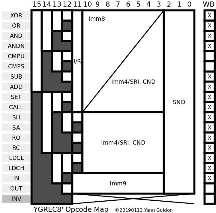
01/13/2019 at 22:23 • 5 commentsYou modify a detail and all the rest crumbles. So after a few "modified details" added up, I had to take a global view again. Here is the result:
![]()
I did my best to avoid fragmentation, while keeping most of the constraints already established. For example, XOR and SET/CALL differ with the bit 15. The first half (8 opcodes) has not changed, but I have moved all the others : SET/CALL are now situated just after the ALU operations, instead of at the very end. The SHL (Shift/Rotate) unit comes next, without Imm8. LDCx also has no Imm8, followed by IN/OUT using only Imm9.
This hopefully simplifies the assembler (which must be rewritten) as well as the instruction decoder (fewer gates).
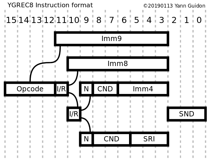
![]()
SND has been moved to the LSB because it looks simpler this way (what do you think ?). This probably amounts to half of the modifications to apply to files and documentation... and also source code because now SND is at the last position !
-
Mister Bin
01/13/2019 at 19:40 • 0 commentsLooking through my stock, I find a bag of 33Ω Russian resistors. The value is a bit weak and there are only 60 of them (the register set has 64 bits)... Time to hit eBay so I can get nicer-looking resistors than the carbon YAGEO 1/2W used for the prototypes. I want to give a crazy, vintage and out-of-this-world look that will stun the novices like the professionals !
After a while though, I start to realise something: why bother with the tolerance? Oh wait, if I bin the relays precisely, then +/-5% resistors will wreck the whole thing...
There are now other approaches:
- Get 1% resistors => more expensive
- Bin the relay with its associated resistor
- Bin the resistors
It will depend on what curious-looking resistors I find...
-
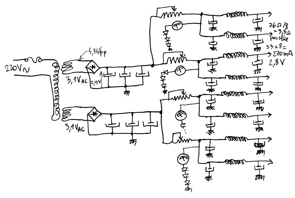
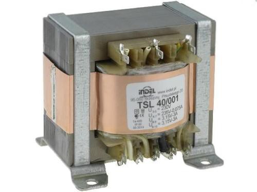
Power supply for the register set
01/09/2019 at 22:29 • 0 commentsThis log continues 43. Data retention times of hysteretic relay latches, I'm digging more into the practical details now.
![]()
First, the fuse (you don't want this to happen) then the transformer: the TSL40/001 from INDEL. The high voltage output is ignored, I only use the 3.15V outputs. There are 2 outputs and each can supply 3A but the register set needs 2.1A (total) so each half will provide only 1A. The extra power can be used for other parts of the circuit.
I have not found suitable Selenium rectifiers for the bridge rectifier. The peak current could be in the 3 or 4A range. I just spotted some Germanium power diodes, we'll have to wait for their delivery to test them. At high current, their drop can become "significant" so I cross my fingers : the output should be around 3V or 2.9V. If we consider the diode drop of silicon diodes, this is achievable, and the Schottky diodes can always be used as a last eventuality.
A few big capacitors filter the bridge's output then the rail is split into two : each half-rail has a small rheostat to "drop" some fractions of volt, and the result is measured with a small solenoid indicator. I'll calibrate the measurements so each branch has the correct voltage and reading. Some diodes drop the voltage so only 60µA flows through the solenoids at the right working point.
Finally this sub-sub-branch is split again and powers 2 "slices", each with their own capacitor-inductor-capacitor filter for the extra smoothing.
So far the only thing I don't have right now is the diode bridges, but I just ordered these parts.
Germanium has a naughty tendency to drift with temperature. The bad way. The behaviour will change with the load and I don't have all the register boards to draw the expected current. I can however simulate one slice (of 8 relays) with 4 resistors in parallel: I have a bunch of YAGEO 39 Ohms 5% 1/2W that will do the trick, the whole set would be emulated by 32 resistors (with each resistor used at half of max. power rating). It's still a progress...
I didn't check enough but... The low voltage secondary is made of 2 windings that are joined in series. I hacked it to make them independent again. Notice the small writings : the 3.15V windings have one pin in common...
![]()
The construction quality is good so it was not hard to separate the 2 windings. I just wish I noticed it earlier !
The resistance of the 3A circuits is very low, I can't measure it with my multimeter. It's going to be very powerful...
-
Improved linear power supply
01/09/2019 at 03:02 • 0 commentsSpoiler alert : read the bottom of the page first :-D
This post is more or less totally not related to CPU design. It's absolutely related to power supplies however !
Let's just jump to the conclusion :
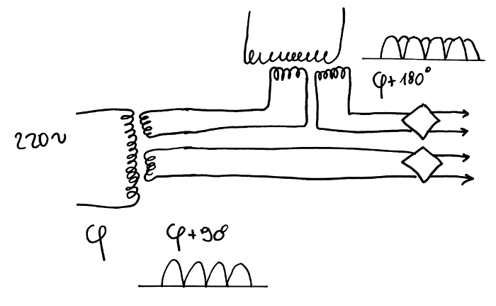
![]()
It's a particularly "overkill" "solution" to an old problem because it requires 2 identical transformers with dual outputs and could in theory output as much current as one.
The advantage is the reduced ripple and a much better cos φ because current is drawn from the mains during the 4 quadrants, instead of only 2. The output ripple is also reduced (and that's the whole point of this circuit ! ) and this is significant for certain types of loads.
The long story :
I finally received one TSL 40/001
![]()
This little Polish device is a well built transformer, usually targeted at lamp/valve amplifiers with 3 secondaries : one is a low-current high voltage output, that I will ignore. The other two are 3A 3.15V, with 18W cumulated power. See the end of 43. Data retention times of hysteretic relay latches for more computations.
I bought one, that I never received. Then I bought a second that I received so I'm considering the next steps. But what if I received the first one ?
Using 2 transformers in parallel will not change much because they would be in phase and they both will require a large amount of filtering capacitors to keep the output ripple low.
Then I realised that the key was the dual, symmetrical but independent outputs. Usually you can wire them to either provide more current (in parallel) or more voltage (series). Or you can power a different circuit. But I have never tried to use the secondary as an isolation transformer, or a de-phaser, though in theory nothing prevents it.
In the above diagram, I use one secondary to de-phase the other secondary by 90°. Because the windings are identical, there should not be any mismatch and the "direct" secondary could be dampened with a small rheostat to account for the extra resistance in the de-phaser. 2 diode bridges rectify the output and only one of them is "active" at a time (one pair of diodes for each quadrant).
This is not as efficient as 3-phase power but it is totally what our grand-dads would have done if they could.
I'm curious to know if this had been already done before. It look like this kind of circuit should be in some textbooks but I have never seen them. The closes I've see is a very large inductor in front of a PSU to smooth and correct cos φ but 2 transformers ?...
I'm happy because this is a question that has been spinning in my head for more than 2 decades and I couldn't resolve myself to "using larger filtering capacitors".
...
Has anybody here seen this circuit before ?
@Bharbour notified me that this wouldn't work and he provided a 'scope screenshot.
![]()
I'm very surprised because this goes against my understanding of how a transformer works.
So I tried too.
And I find no phase shifting either ! The output mostly copies the input.
I'm so disappointed :-D
-
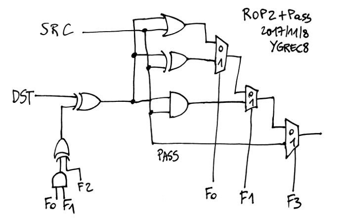
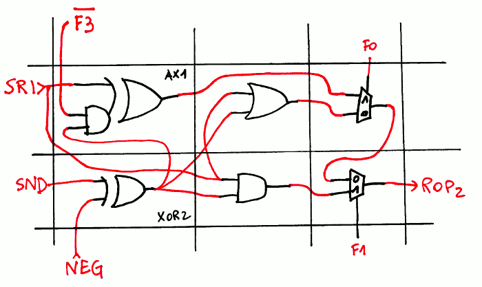
Improved ROP2
01/03/2019 at 23:23 • 5 commentsIn the log 5. YGREC in VHDL, ALU redesign I show how the ROP2 unit shares gates with the adder.
![]()
The "Pass" datapath is quite annoying with the 3rd multiplexer so I moved it upstream, taking advantage of the 3-input gates.
![]()
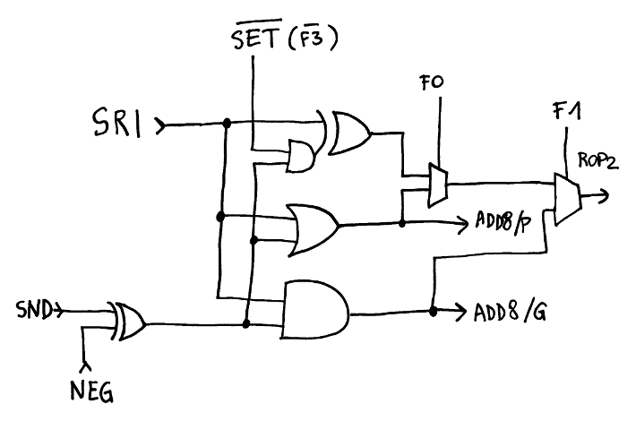
The merged gate is now a type AX1 and saves a tiny bit of latency on the ROP2 critical datapath, as well as one gate. This is valid for the ProASIC3 as well as other FPGA, less so for discrete or MUX-based technologies (such as relays). This change is significant enough, however, to justify a redesign of the opcode map, following these constraints :
- The SET opcode must "map" to the XOR opcode, F0 and F1 must be identical but F3 (or F2?) must be opposite. There is no constraint with CALL anymore because the datapath has a couple of bypasses.
- Computing the NEG signal should be a bit easier and I want to get rid of the XOR gate. I re-organised the opcodes so the function is MAJ3 (which must be added to the #VHDL library of ProASIC3 gates)
The new mapping is :
![]()
This means I have to redesign the ALU "a bit" but with more emphasis on place&route. The above new circuit is easy to process by hand. There are however a few details that change with the order of the bit, during comparison. From the previous version of the ALU8 code:
-- Initial XOR of the operands
XOR_DST <= (7=> negate_DST and not compare_signed, others => negate_DST);
XOR_SRC <= (7=>                    compare_signed, others =>        '0');
DSTX <= DST XOR XOR_DST;
SRCX <= SRC XOR XOR_SRC;
Bus names have changed since 2017, DST=>SND and SRC=>SRI. The code says that SRI(7) is XORed with the control signal "compare_signed", and SND(7) with its inverse. This adds an inconvenient corner case that I'd like to get rid of... It doesn't affect the critical datapath a lot but placement gets trickier.
I'll "tweak" that later but at least the SND input could be inverted by a XOR3 instead of XOR2, or the specific NEG input could get a special treatment.
Layout is pretty easy:
![]()
That's a good base for the ADD8 that connects to it (I didn't show the P, G and XOR outputs).
One nice thing with this kind of pre-routing is the opportunity to spot optimisations for later in ASIC. For example: there are MUXes driven by the same control signal so they can share a buffer and inverter with a direct neighbour.
-
Improved Shuffling Unit
01/03/2019 at 21:07 • 0 commentsThe pressure on the ISA increases and I am already forced to squeeze 2 instructions in the IN and LCDL opcodes. Naturally I'm looking at the shifting/shuffling/barrel shifter and the 4 opcodes.
Things have changed since the last time because the short immediate is now a signed 4-bits field ! This means that an opcode such as ROR can encode both left and right directions, saving space in the opcode map.
SHL, SHR => SH
ROL, ROR => ROT
There are also two other desirable variations :
- Rotate through Carry (not sure it is really necessary with all the predicated instructions ?)
- Shift Arithmetic
With Imm4, there is no use for the Imm8 field now as well, which saves another bit. The shifter will use only two opcodes by moving the arithmetic flag/carry flag in the R/I8 flag.
What could these opcodes be used for ? They should remain reserved for now but I can already see the Imm8 extended back to 9 bits for the IN and OUT opcodes, leaving one remaining free opcode slot...
-
Assembly in VHDL works
01/01/2019 at 16:04 • 0 commentsThe latest archive upload shows the new assembler, which just passed all the self-tests. The few corner cases gave some difficulties but they were solved.
Part of the self-test includes throwing "stuff" at the assembler and disassemble it, to see if the parser chokes on anything. Of course this is not perfect but most cases of user abuse are covered.
The other part scans the WHOLE INSTRUCTION SPACE. The instruction is disassembled, reassembled an re-disassembled to check discrepancies. This is where the ambiguities become obvious.
- Instructions with small immediate values are always assembled to Imm4 but it is also possible to encode them in binary as Imm8. This is a sort of "funnel" and 824 Imm8 codes are converted to Imm4 codes.
- ADD SND Imm4 increments the Imm4 field when it is not negative. This creates an additional mismatch with ADD SND Imm8, which creates an additional "funnel" of 64 codes.
- LDCH and LDCL don't take conditions into account, which creates another "funnel" of 3712 codes.
All these test ensure that no "blind spot" or undefined behaviour exists, not just in the assembler and disassembler, but also in the ISA itself.
Overall, VHDL is perfectly capable of assembling and disassembling instructions with only the basic feature set. It's not the easiest language but the Ada legacy helps a lot ! Thanks to GHDL there is no need of an external software module and this package ygrec8_asm adds a lot of convenience in the simulator, emulator and debugger !
-
Assembly syntax
12/24/2018 at 07:01 • 0 commentsI have to rewrite the assembler and disassembler... so here is the census of the instructions and their syntax, in order of complexity :-)
- NOP => 0000h
INV,
HLT => FFFFh - OVL Imm8 => FF........h
- IN,
OUT SND Imm8 => (no SRI) Ch snd i/o Imm8 - LDCL,
LDCH SND SRI => (no Imm8) Dh snd l/h ..... sri (condition not supported yet) - XOR,
OR,
AND,
ANDN,
CMPU,
CMPS,
SUB,
ADD,
SHR,
SHL,
SAR,
ROL,
SET,
CALL SND Imm8/Imm4 [cond2]/SRI [cond3] => (see diagram)
This should help structure the code :-) There are 4 special cases to check, and then it's all very orthogonal.
- NOP => 0000h
-
Data retention times of hysteretic relay latches
11/06/2018 at 04:58 • 1 commentSo far I have not actually measured how long a hysteresis-based relay latch could hold a state. So I'm doing it now.
I have set up a little circuit with a RES15 relay (36 Ohms), a matching series resistors (39 ohms), a capacitor to set the state, and a LED to show the state.
The circuit is powered by a digitally controlled PSU set at 2.8V (mid-way between the 2.1V release voltage and the 3.62V latching voltage). After a while, the circuit draws 33mA (some heating occurs in the coil).
I have no idea how long the circuit can stay latched so it's not possible to use my multimeter (it would go into power-saving mode after some minutes instead of beeping). I have no timer either, so I connected an LED that would light up when the relay is released... and I count time manually :-D
Unless the register set is held in standby state during a debug session, I can imagine that a register would be toggled at the very least once a minute and the experiment is running for 3 hours now. The possible cause of perturbation in this test would be the poor wiring quality on the solderless breadboard, so I stay away from it to prevent any minute wiggle.
Retention of 1 bit requires 92mW so 64 bits (the YGREC8's register set) would draw 5.9W alone... This register set needs a separate power supply that is very stable and well filtered : 2.8V (5%) at 2.1A. Early experiments (with the YGREC16) have shown that the system is not stable if the latches' supply is shared with other circuits, which create a lot of switching noise.
I don't want to use a modern PSU so I'll go for the old good way : an AC transformer, a diode bridge and a large filtering capacitor. A very big capacitor is not difficult to find (10000µF at least, more is better to keep the ripple as low as possible), the diode bridge is possible (there were selenium rectifiers in the 1930s, each plate stands about 20V) but a low voltage transformer is a different story today. I'm not sure I can find a transformer that can provide 3VAC under at least 2A (more is better). At least, I can finely adjust the input AC with an auto-transformer.
"Back in the days" when tubes/valves were kings, radio sets would provide a low voltage, "high current" output to power the heater(s). This is something to explore but what I have seen so far is 6V or 12V output, not 3V and only 2 wires.
Another alley to explore is partition : there are 8 bits that can be written at any moment (plus PC) so 8 subcircuits (one per bitslice) are possible, each with their own power source. Partition would be along the bitslice, not per register, because each write would create noise on 8 bits simultaneously and the strategy is to spread those spikes evenly. So each bitslice would have at least a local filter (capacitor + inductor) that can provide a clean power at 270mA. A local diode can also drop the current if needed.
If each bitslice has a local power input, the transformer can be partitioned into multiple smaller transformers. The bridge rectifiers become smaller too.
If I can find suitable 3V AC transformers, then adding the drop of a silicon diode bridge gives the right voltage : 3×1.4=4.2V, 4.2-(2×0.7V)=2.8V
I remember some old 1A bricks with a selectable output voltage : 3V, 4.5V, 6V, 9V, 12V. Inside, a PCB holds four diodes and a 1000µF capacitor, and the secondary windings were probably multiple 1.5V or 3V in series. I could rewire that in parallel to provide a stronger 3V output ...
test interrupted after 3h46m due to human error...
Test is restarted : 6 hours and no sign of weakness. Shall I call this experiment a success ?
In this circuit, the coil draws 33mA under 1.38V only. Half of the power is dissipated by the 39 ohms resistor (46mW). A different type of relay (with higher coil resistance and higher voltage) would decrease the overall current and ease the selection of the transformer.
The resistor is another problem and I wonder how to void it.
I stopped the test after more than 33h of flawless latching : the hysteresis is validated. A very stable power supply is the key!
For the power transformer, I just discovered the TSL series from INDEL. Two references (TSL40/001 and TSL100/001) provide dual 3.15V outputs at 3A each, that's about 18W (I ignore the very high voltage output). TSL100/001 also provides 5V and 6.3V at 2A each. The cheaper TS20/24 provides 9V@2A but 3V@1.5A only... So I ordered a TSL40/001.
What should be the maximum tolerable ripple on the power supply ? This relay latches at 3.6V and releases at 2.1V, the resistor of equal value as the coil nearly doubles the tolerance to ripple, and the margin is 1.5V. A ripple of 100mV or 150mV max. would be tolerable... But from experience : each relay has a bit of variation and this significantly reduces the margin of an overall group. This is explained there : https://hackaday.io/project/14628-ambap-a-modest-bitslice-architecture-proposal/log/45438-pre-biased-or-hysteresis-relay-logic
The 8 bitslices will have their own filter, to power 8 bits, and they can have a little resistor to adjust the current-voltage on the bitslice, so a batch of 64 relays can be "binned" into 8 lots of relays with very near characteristics. This was the purpose of #ReTest-RPi but I have not progressed on that front... Time to revive it !
-
Imm4
11/01/2018 at 06:19 • 0 commentsLet's break orthogonality again !
Imm3 is pretty lousy and can make only very short loops, 4 instructions maximum. Where and how can I get more bits ?
The condition code is a good candidate: there is one "negate" flag, and 3 source bits. 4 sources are external arbitrary, configurable signals, but are they required ?
Let's drop those extra conditions in the "short immediate" format so Imm3 becomes Imm4. The extra conditions are still available with the register form, because there are only 8 source registers. And I don't want to get rid of the extra conditions because they will be very handy later, when used as a microcontroller: that thing is meant to deal with I/Os and it's a nice feature to inherit from the CDP1802 ("The 1802 has a single bit, programmable and testable output port (Q), and four input pins which are directly tested by branch instructions (EF1-EF4).").
The diagrams must be updated or redrawn and the assembler must be modified...
YGREC8
A byte-wide stripped-down version of the YGREC16 architecture