The previous log 139. Carry on made the case that a prefix would be necessary to solve a pretty difficult problem caused by the lack of opcode space.
Such a prefix would eat some of the INV opcode space that is reserved so far. It's only a tiny dent though, and there is some room. So why not have a more potent prefix opcode ?
The prefix could select the source of the carry bit, for example, so we can reuse the whole condition logic and corresponding fields (that's 4 bits though I'm not sure all will be useful). This value would be latched only for the next instruction. That will make exceptions very fun to handle.
The prefix can also change the destination for the next instruction, to make YGREC8 a semi-2R1W architecture when needed (this could relieve some pressure during coding). So the SND field will be latched for later.
I have no idea what the I/R, I/R2 and SRI fields could be used for, so far.
I/R should not be touched, to keep the INV opcode. But then we lose an IMM8 at least.
SRI does not seem to have valuable information so far. Not sure it could hold MSB of IMM4 value.
I/R2 could select a different prefix. Some reserved opcodes will be required to return from exceptions for example.
The first prefix uses 2 existing fields and leaves 3 bits in the middle.
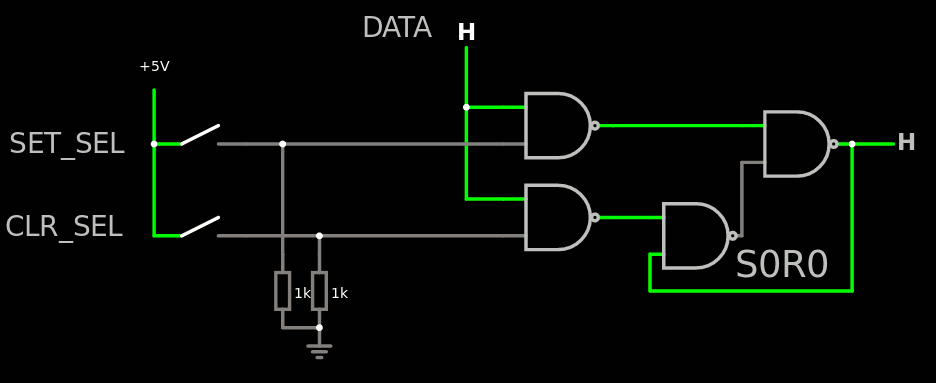
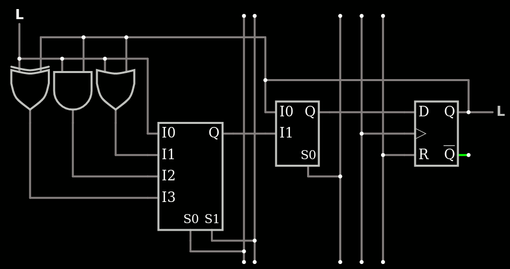
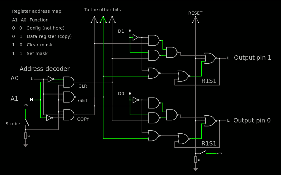
When Y8 is integrated in a chip as a building block of a SoC or a microcontroller, the IO space implements some pin-altering registers, usually named GPIO. So you have configuration registers, read register and output register... This last one is often the tricky one.
In the simplest cases, only a direct output from a DFF or Latch is implemented. This increases the code size and execution time because when you want to modify specific bits, you first have to read the previous port state (or read it from a cached copy somewhere), then mask the unwanted bits and/or OR the others then finally write the result. And code space is often a premium, particularly with only 256 addressable instructions !
Some more modern chips provide alternate addresses for the output registers, providing additional features such as SET, CLEAR and TOGGLE functions. I start from SET and CLEAR because that's what I was discussing lately. They are indeed implemented straight-forwardly by a Set/Reset flipflop using only 2 NAND2 gates, or 8 transistors in CMOS (2 in RTL/DTL/CTL).
So I take a basic S0R0 flip flop and add two NAND gates to selectively enable the clear and the set. This way, you just write a 1 to the bits you want to clear or set on the given port. Try by yourself, it's easy :-)
Total : 4 NAND2 gates (16 transistors per pin), and they can even be paired to use smaller footprints with standard cells.
Note that the DATA signal is latched from the Y8's register set's read port, it is pretty stable for a while (until a new instruction is fetched). The _SEL signals get decoded and take a bit longer to come alive, and they are only short strobes after the data has settled (otherwise it's a hell, you have to distribute the main clock signal everywhere...).
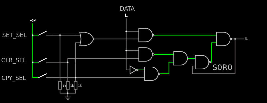
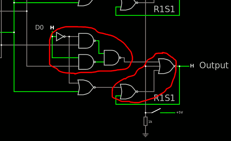
The more normal copy though is a bit more complex but having the 3 functions "copy", "set" and "clear" amount to implementing a transparent latch with clear and set. So I'm mostly reinventing the wheel... with the small detail that the clear and set must be controlled by the input data (which acts as an "enable" pin) so it does not conform to a classic standard cell. Thus, let's dive in and have a look at the circuit made with CircuitJS:
The "copy" function is quite easy for the "set" half : it is congruent with the "set" function indeed. So it's managed at the decoder level.
But the system must copy the Zero value and that's the tricky part. It requires two more AND and an inverter.
The structure with the 2 NAND2 converging to the AND is reminiscent of a XOR structure, except there are 3 inputs instead of 2. But the 3 gates could be merged into a single standard macrocell.
Note also that the CPY_SEL signal can be bubble-pushed so the inverter on the data disappears. But this creates a OR which needs its own inverter anyway...
There is this alternative version with some bubble-pushing, still using a non-inverting gate (AND) which has its own inverter. But the total amound of inverters has been cut in half. Sigh.
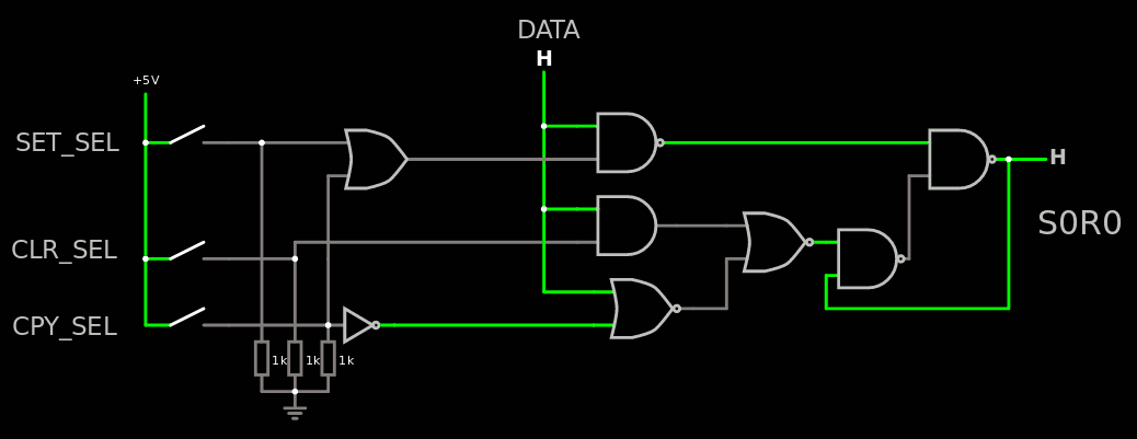
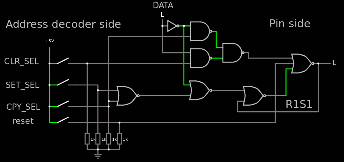
For each bit of the port, there are 2 pairs of gates that can be merged into a single more complex standard cell each, and 2 gates that remain lonely... That's a total of 26 CMOS transistors, and a bit more for a general reset. To implement the general reset one needs a R1S1 cell instead and rebuild everything but the general reset signal will do its work cleanly.
So here is the final result : 1 inverter, 3 NAND2, 2 NOR2 and 1 NOR3 per controlled bit, and you can play with it there.
Et voilà.
There is a function that is one order of magnitude larger to implement : the "toggle" function requires storing the last value in the port, which needs a full-blown DFF. It's sad and it's something I wish the Raspberry Pi implemented to make #SPI4C practical to code.
Anyway the current features are already nice and compact, decoding is rather simple, the timing should be good as long as DATA remains stable before and after the x_SEL pulse. I could add a state in the FSM to ensure it, at worst.
This means much more transistors, more high-fanout signals, more clock and activity everywhere... more power just to add a small "toggle" feature. So I think that the previous asynchronous circuit is a decent compromise.
I thought that having a carry flag would be enough to solve multi-precision arithmetic codes. It is not.
The conditional execution of instructions does not solve it either.
It is really necessary to have a ADC opcode that takes the carry bit as an input (and SBB as well).
And this is very worrying because the opcode map was frozen and now I need 2 more opcodes while all the opcode space is taken
._._.
It's not that multi-precision addition is expected to be very common but when it occurs, it gets ugly : it takes multiple instructions and registers, it loses orthogonality. I have covered a possible trick at https://hackaday.io/project/27280-ygrec8/log/199934-add-with-carry-the-macro but I don't like it.
ADC is easy to implement : it's just a AND gate between the output of the carry flag and the carry input of the adder. SBB is almost the same.
The real problem is that I thought it was not necessary. The opcode map has been frozen and now I need 2 more opcodes. I could dump CMPU and CMPS but their "no writeback" behaviour will increase register pressure or bloat code in common code sequences.
Any more complex reorganisation will break a lot of code as well as the electronic devices I have already built. It's not impossible but probably not worth it, as the opcode map has been thoroughly polished.
The last solution I see is ugly in the principle, but convenient : create a "prefix opcode" that enables the carry input.
An I/O port address could be attributed to this function but it would read or destroy a register. Anyway : OUT 0 PC looks alluring.
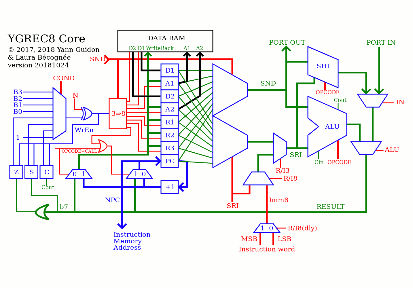
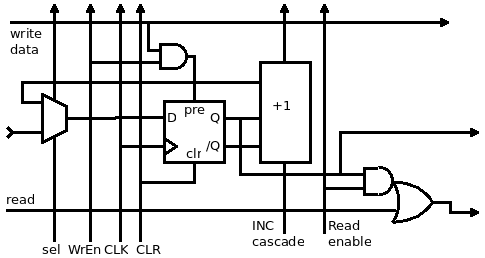
It seems that the "main schematic" below, used as the project's avatar image, is not obvious enough, at least before zooming in enough.
@Ken KD5ZXG was not sure how to interpret/decypher the upper-left side.
I see YGCREC8 mux between Carry Sign Zero Always and the lower four bits of B. What is B? I get what Write Enable and N are for, but how do these interact with the tested condition to drive some rectangle called 3=>8 that I might guess 8 way mux if you hadn't already drawn other mux with the proper symbol. Maybe the 3=>8 rectangle is just a decoder? I've got a condition mixed with N thats probably one of the 3 selects, a write enable thats not clear how it works (chip enable?), SND whose purpose remains a mystery drives some other select bits? Enlighten me, cause I'm clearly not getting it.
So here is the explanation.
The 4 basic conditions are ACSZ, as already obvious. I now use the alphabetical order for convenience and mnemotechnic help.
The 4 extended conditions are optional and user-configurable: either fixed (if you have 4 input/GPIO pins or other internal signals) OR you can implement a set of Special Registers that select the source of each condition bit. This is one of the tricks inherited from the YASEP.
The home page says :
The COND field has 3 bits (for Imm4) or 4 bits, more than YGREC16, so we can add more direct binary input signals. All conditions can be negated so we have :
Always
Z (Zero, all bits cleared)
C (Carry)
S (Sign, MSB)
B0, B1, B2, B3 (for register-register form only, we can select 4 bits to test from user-defined sources)
So this extra condition bit allows extensions for later, which could speed up some IO intensive algos, such as bit banging. "B" means "bit", it's not a register per se (though it must be latched before to prevent race conditions) and it is user-defined wires. They could be front panel switches, synchronous or asynchronous data over 1 or 2 bits... or some condition inside the extensions blocks like UART ready/overflow/whatever status bits. I was a bit inspired by the CDP1802 on this, I admit.
The "Never" condition could be mapped to another bit/wire/condition but I don't want to play this game yet. ARM mapped this to an extension to the instruction set but YGREC8 is too young for that gymnastics yet.
... Maybe the 3=>8 rectangle is just a decoder?
Yes, once the condition for writing the destination register is determined, it is sent to the appropriate destination register for writeback. I should have made it clearer but the drawing is already pretty crowded :-)
The register set uses latches, and not DFF, to cut the register set power/area/cost in half. Imagine routing the clock signal to 64 bits and only updating 8 (or 16) every time... The diagram misses a buffer latch on the result datapath btw.
I'll try to summarize :
First the condition must be evaluated. It is by default 1 : enable. The XOR can negate the condition when needed, directed by the relevant bit in the instruction word (in red). The condition can be any of A/C/S/Z/b0/b1/b2/b3 (the B conditions are optional as noted above). So it is quite simple : we have a bit that is usually 1, but also selectively cleared.
The condition is valid at the output of the XOR. Then this signal will
enable the update of the C/S/Z condition flags
go to the 3=>8 decoder to enable and select one byte of latches, so the relevant register (indicated by the SND field) is written (or not).
In the log 129. Counters strike ! I started considering the new version of the "counters". It's easier said than made and the many clock domains don't ease the design. But I managed to draft one "bit":
Each byte can be read with one byte select per counter (but the latency is quite high as the data ripple through many gates). Writing is another story because it's asynchronous so a byte clear precedes a selective set. Each byte has their own clock domain, selected among various sources, including the preceding counters. And the counter's value comes either from the local incrementer or the previous counter's value, for the cases of arbitrary frequency dividers (think: baud generator as a trivial example, the previous incrementer is left unused in this case).
This is quite scalable, the size of the pool of counters can be configured at will. A 8×8 bits block seems like a good compromise but nothing keeps one from changing that.
. . . . . . . . . . . .
Looking further, 2 main concerns arise:
Latency : I don't want the I/O space to be too constrained or constraining. There might be a cacophony of wires, registers and decoders that would probably slow everything down. So let's consider the I/O space as "mostly asynchronous" from the core's point of view. This means that IN and OUT should have a "completion" flag that lets the core resume operation once the IO is done. Which means I must adapt/change/update the instruction's FSM...
The register map. So far I have identified that each counter byte could have 2 addresses: one for read and write of the value, the other for control and status. Thus there is no constraint on the total number of counters: implement as many as you like. However, timing and scheduling becomes critical at this point so look at the previous point.
Now that I have an assembler, how do I upload the program into the core ?
The TAP (Test Access Port) allows one to upload data, instruction by instruction, then make the core run them. However this is quite complex and not suitable for autonomous operation, like, when the core works alone.
One thing I would loooove is to hook the circuit to a serial port of my computer and then cat a binary file through /dev/ttyS0 to the circuit. When 512 bytes are transferred, the processor starts the uploaded program. It's convenient from the user's point of view, though it doesn't allow full debugging and requires baud generation circuits. Some sort of external adaptation circuit on a dongle must be designed.
Another interesting situation would be that the TAP circuit itself goes to fetch the program by itself. Usually it comes from a SPI Flash device, and I have already developed such a system in 2014/2015 for #WizYasep.
I am familiar with SPI Flash devices: #SPI Flasher implements a few protocols already. SPI usually works with 4 signals :
MISO
MOSI
CLK
SEL
Compare this to the TAP interface:
Din
Dout
CLK
R/W
/Reset (optional)
It looks quite similar, right? Furthermore, the TAP contains the shift register and the other circuits that write to the program memory, which is indexed by the PC register (the latter conveniently wraps around to 0 when the upload is over, and signals the FSM to start running said program).
So there are already about one half of the circuits in place for autonomous loading, now the trick is how to hack the existing system to add the new features.
First, the Y8 interface needs to know the operating mode. So far, the TAP had only one mode so the question didn't arise but we have identified 3 modes, that would be conveniently selected by weak pull-up/down resistors on the pins:
TAP mode : R/W low, CLK low (?)
External/slave programming mode : R/W low, CLK high (?)
Autonomous SPI programming mode : R/W high
It starts to look like what modern FPGA provide...
Usually, the R/W pin is pulled up by an internal weak resistor, which is overridden by an external upload/control device. The default behaviour is to get the stream of 4096 bitts from external SPI storage. I'm not sure yet about the CRC/scrambling, which can be designed/added later, but should not remain an afterthought for ever.
The state of the R/W pin is sampled by the FSM during the Reset sequence, just after the /Reset pin is brought high. Note that the TAP is still functional even when the rest of the chip is held in RESET state, since TAP as its own reset sequence and clock domain.
Note: the TAP used to have 3 pins only (plus external RESET though it could also be controlled from within the TAP registers). See https://hackaday.io/project/27280-ygrec8/log/182563-tap-pins for the diagrams. Now, in addition to the previously defined interface, the external debug/upload device must control the /Reset pin to take over the internal FSM and prevent conflicts with the internal operation. The minimal number of pins for the probe is 6 but more become desired:
Din
Dout
CLK
R/W
SSel (open collector)
/Reset (open collector)
Vtarget
GND
It's on the "high tier" of the pin count range for probes but that's the price for sharing a SPI bus between 2 masters. It's also for safety due to the uncertainty of the support of "half-duplex" mode by SPI Flash chips. I added these 2 pins:
The debug probe would certainly want to access the SPI Flash for programming, and the SPI Flash should not interfere with the normal TAP operation. A separate pulled-up SPI Sel pin (SSel) becomes necessary so the SPI Flash is deselected during TAP operation.
I also added Vtarget because the TAP probe shouldn't operate if the target circuit is not energised. Some voltage translation buffers will ensure electrical integrity, prevent "ghost powering" through pins' protection diodes, and the probe must be sure that the target is correctly powered.
I know it's getting more complex but not everything is required in the beginning. Maybe I'll find a trick to remove one of the signals because each pin is a precious resource...
Y8asm is a 2-pass assembler written in VHDL.
It transforms source/assembly language .y8 files
into .hyx files suitable for flashing/emulation.
The VHDL code is compiled and elaborated with GHDL by the
provided build/test script, and generates an executable program.
Pre-processing
The program can't include files or manage macros. Use external programs such as cpp or m4. You could also concatenate
source files with cat to a temporary file.
Program invocation
The program runs on the command line interface
or in a script. There are 3 active parameters:
• Input file name: -gname
$ ./y8asm -gname=example.y8
will assemble the file named example.y8.
The output file name is derived from this parameter, with the .hyx suffix.
The output file will be overwritten without a warning.
• Symbol table output: -gdump
$ ./y8asm -gname=example.y8 -gdump=yes
appends a dump of the user-defined symbols in the comments at the end of the .hyx output file.
The dump also contains the number of times the symbol has been referenced (though it might be over-estimated because it includes both passes). That's still convenient if you want to clean up your source code and prune some useless lines.
The option -gdump=full dumps all the defined symbols, including the reserved words, keywords, opcodes etc.
• Maximum Symbol Length : -gmax_sym_len
$ ./y8asm -gname=example.y8 -gmax_sym_len=12
changes the maximum length of symbols (labels, identifiers etc.)
from the defaut 16 characters to 12 characters.
Basic Syntax
• Comments start at ';' and remove the rest of the line.
• All the symbols are translated to upper case during parsing.
• The symbols can not be redefined. Unless they are in a nested context (not yet implemented).
• User's symbols have a range dependent on the VHDL simulator,
"at least 32 bits". This is practical for intermediary values since
the assembler checks each range for every instruction field.
• Identifiers can contain the following letters: '_',
'A' to 'Z' and '0' to '9' (but no digit at the first position).
• Separators are space' ', comma',',
horizontal tab, and ASCII character 160 ( in HTML).
• The dollar sign '$' represents/returns the value of the current address.
• Numbers are decimal by default. Binary numbers have the b
suffix and h is the hexadecimal suffix.
• Numerical computations ("expressions") are always between parenthesis, to avoid precedence. The assembler supports the following arithmetic operations:
'+',
'-',
'*',
'/',
'%'. VHDL does not allow easy boolean operations on integers,
unless you go the std_logic_vector route, but I can't change the standard... I'll add later if needed.
• By default, code is assembled starting at address 0. Don't forget to ORG if you need otherwise.
Pseudo-instructions
The assembler provides some housekeeping commands that greatly help even basic programs.
• END
Ends parsing of the file. The source file can contain any garbage below this line.
• DEF
DEFines a new user symbol.
The line
DEF plop 42
defines the symbol "PLOP" and assigns
the value 42. The symbol "PLOP" can be used later in the source file, and even before for instructions and DW.
See the -gdump=yes command line argument to list
all the user-defined symbols.
• Label:
The line
plop:
is a shorthand to the line "DEF plop $".
There is no separator before ':' and the label must be alone on the line.
• ORG
Change the address to which the next instruction will be assembled/stored.
ORG 42
means that the next instruction will be stored at
address 42.
The value may be a number, symbol or expression, but can not be post-defined or have a value lower than the current address.
• DW
DW 42
will output the value 42 to the instruction memory space, as if it was an instruction.
Just like an instruction, it is 16-bit wide and can have a post-defined value.
Instructions
The assembler pre-defines the following keywords as elements of an instruction:
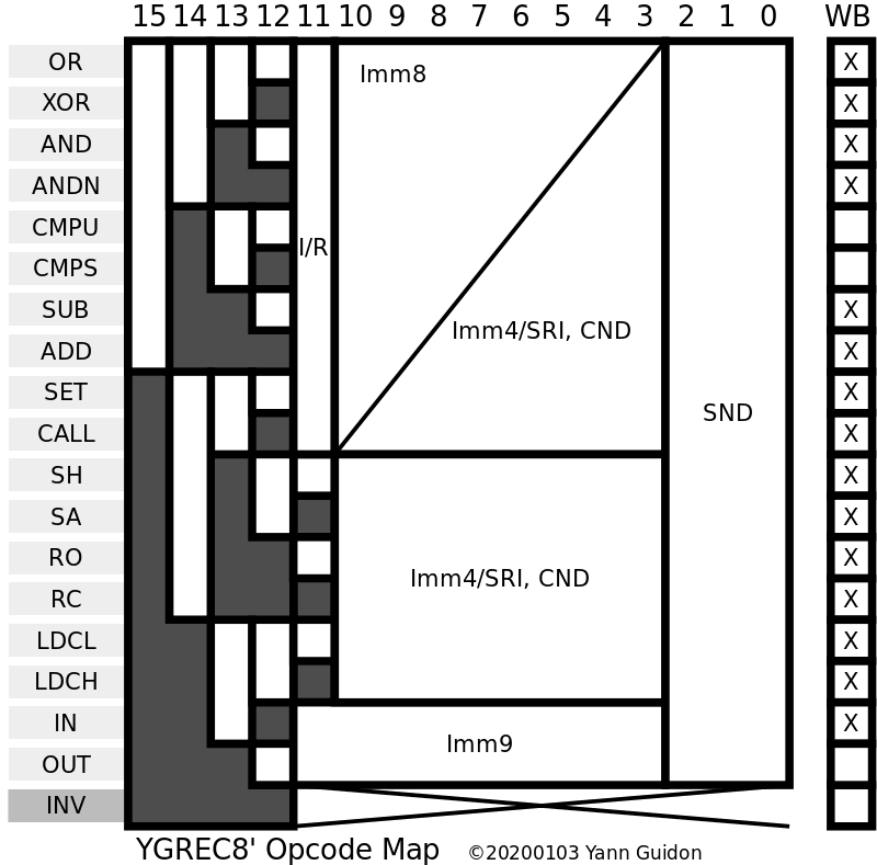
Follow the opcode map to see which operations are possible:
The instruction's textual format follows the binary format
(except the condition which is a suffix).
• No operand:
"HLT",
"INV",
"NOP"
Examples:
NOP ; do nothing

HLT ; put the core in sleep mode until the next IRQ

INV ; trigger a trap/reboot/panic
• One immediate operand and a register:
"IN",
"OUT"
Examples:
IN 67, D3  ; get value from IOspace at address 67 and write register D3

OUT 45 A1 ; Put the value of A1 into IOspace at address 45
• One short immediate or a source register, a destination register and optional condition:
"LDCH",
"LDCL",
"RC",
"RO",
"SA",
"SH"
Examples:
RC  1  D1      ; Rotate register D1 through carry by 1 position (left)

RO -3  D2 IFNC ; Rotate register D2 by 3 positions (right) when the carry bit is clear

SA  R1 A1      ; Arithmetic Shift of A1 by R1 positions

SH  R2 A2 IFZ  ; Logic shift of A2 by R2 positions if Zero flag is clear
• One long immediate and a destination register, OR One short immediate or a source register, a destination register and optional condition:
"ADD",
"AND",
"ANDN",
"CALL",
"CMPS",
"CMPU",
"OR",
"SET",
"SUB",
"XOR"
Examples:
AND 123 R1 ; bit-mask R1 with byte 123

ADD -76 R2 ; subtract byte 76 from register R2

SUB  95 R3 ; Subtract R3 from byte 95 and put the result in R3

ADD 1 A1 IFC ; increment A1 by short 1 if the carry bit is set

ADD 0 A1 IFC ; INVALID !  \ short add increments positive
ADD 8 A1 IFC ;   VALID !  /     immediate values by 1             ;                 to extend the range of jumps

ADD D1 A1 IFN ; Add D1 to A1 (result in A1) if the Negative flag is set.
A backwards loop could then contain 8 instructions (including a test for the end of the loop) but the forward jump can only skip over 7 instructions, despite the ability to encode the constant 8 when dealing with the PC register.
The offset 1 is still possible and this represents the next instruction, which would be trivial to execute otherwise. And the offset 8 points to the 8th instruction after the skipped block, it's not the size of the skipped block.
At least it's now impossible to do a pointless loop such as
ADD 0 PC ifnz ; spin endlessly doing nothing
To achieve a more practical goal, the operand should be the NPC, or PC+1, which is being computed at the same time as the addition. But this creates a whole lot of troubles, in particular:
if we compute PC+2 then the backwards jump will only reach 7 instructions
Timing becomes too tight, since the pipeline must choose between PC and PC+1 depending on the imm's sign
This will require a stall cycle, and there is already one because writes to PC must discard the prefetched instruction.
At this point, the "short add trick" requires only a few logic gates (to detect the opcode, the format and the sign of imm4, detecting the PC register is not even necessary) and no deep modification of the state machine.
Trying to squeeze one more instruction, to skip 8 opcodes, would complicate the whole circuit with quite little benefits...
Some pretty things are there though it's still missing quite a lot:
The assembler is not complete: it misses some keywords, thorough tests, padding, proper symbol definitions and backward patches... update 20211118: VHDL assembler is mostly functional. more tests, doc & examples are welcome, as well as nested expressions.
The ALU8 is more-or-less working, the tests run but find an error.
TAP is incomplete and more debug infrastructure is required.
Some files have been split and/or moved around
the gates library #Libre Gates project is still somehow evolving in parallel, in a soft fork that I'll have to reconcile.
The core is still not complete... there are still many things to manage under the hood. But what works works well :-)
And having a proper assembler helps a lot too. No more estimates, it's now possible to test and reproduce ideas! So I think it's the priority for the next days, then I'll go back to #Libre Gates so I can fix the ALU and progress on the TAP, which is critical to enter programs, control the core and read back its status...
The Shift unit and the register set will then be quite easy to design, I think.
Work is progressing nicely on the new assembler. This also allows me to find some corner cases that I didn't consider carefully yet. Let's look at the existing disassembler:
    if OPC=Op_CALL and SND=Reg_PC then
      if Imm9="111111111" then
        result(1 to 3):="HLT";
      else
    result(1 to 7):="OVL " & SLV_to_Hex(Imm8) & "h";
-- /!\ bit 11 not used ?
      end if;
      return;
    end if;
The HLT (halt) opcode uses all the 9 bits but the OVL (overlay) only uses 8, since only a byte can be managed by the overly register.
The 11th bit is not handled so there are 3 ideas that come to mind :
extend the immediate field to work with IMM9 like IN/OUT (simplest)
consider the R/I bit so the OVL instruction can use a register argument as well (useful to deal with multiple or indirect overlay numbers)
create a new instruction that provides another functionality (which ?)
 Yann Guidon / YGDES