Yann Guidon / YGDES
-
Towards a better assembler, still in VHDL, sans Lex & Yacc
11/06/2021 at 05:04 • 0 commentsMore and more, I'm looking at the YASEP's JavaScript framework and want to reuse it to develop better programs for the YGREC. This would be great to explore the practical limitations of the Y8...
Then I realise how outdated, clunky, messy and unmanageable #YGWM still is :-/
And I don't want to use C stuff : I have committed to using only bash and VHDL.
And here we are...
The project already provides YGREC8/ASM/Y8asm.vhdl but this is useful only for inline, context-less instructions. I want to create/write/assemble/run real programs, generate .HYX files and load them for simulation.
Without EVEN starting to deal with all the parsing, two critical parts are already required :
- The .HYX filter (only a C in/out filter is available so far)
- The symbols table.
IN VHDL.
I think I'll start with 1. because the algorithms are already written in C and JS.
Then, I'll deal with the dynamic allocation of symbols. I have chosen to use a unified table where the opcodes, the pseudo-opcodes, the unknown symbols and the defined symbols are kept together, to keep the complexity low and ensure there is no "shadowing", such as redefnition of opcodes, numbers etc. (as was the case in the buggy YASEP assembler in JS, where I lazily used string substitutions as a shortcut and it could totally break everything...)
Update: drawing from the YASM experience, the assembler should use a collection of dictionaries, first the pseudocodes and opcodes, then the local symbols, then the global symbols, eventually more, such that function nesting becomes possible (for example) and important things don't get re-defined. At first, only a global symbol table will be defined but more should be able to be allocated and de-allocated. A kind of linked list of symbol tables will ensure precedence.
Ephemeral Local symbol tables will be useful for the macros, for example. In this context, some inspiration from C syntax will help: the pseudo-symbol '{' would create one table and '}' destroys the last created.
Preprocessing would use m4.
_________________________________________________________________
OK, as usual, I say something then do the contrary, so here is dictionary.vhdl.
"Methods" are provided to create a dictionary, look it up, add a symbol and flush the whole dictionary. The idea being that there is one dictionary per context and the contexts can be stacked with "{" and unstacked/flushed by "}".
That will make the assembler way easier to write, and now I need to handle .HYX files...
____________________________________________________________________
20211112: a few days of passionate work and YGREC8_VHDL.20211112.tgz is now available !
It's missing at least two important features: arithmetic expressions and symbol definition&update. Anyway it's starting to be useful to write simple programs. It's a bit bloated and requires some refactoring but it's only 741 lines so far (not including a few external packages).
I have so far been very, overly confident maybe, about the use of the ISA and now I'll be able to prove its worth.
____________________________________________________________________
20211118: YGREC8_VHDL.20211118.tgz provides a refactored assembler that supports more features and works better. I am now able to write whole programs!
And it's all written in VHDL, 700 lines so far.
-
Add with carry : the macro
11/03/2021 at 02:52 • 6 commentsThe Y8 core has a carry flag but no ADC opcode. That's a compromise, turned into a fact now. So how do we perform multi-precision add/sub ?
The first way uses the conditional form that can contains a small immediate. This can skip an instruction that increments the MSB but then comes the problem of the eventual secondary carry, which requires another conditional test.
Another way uses the rotate-through-carry instruction. Again, secondary carry and all...
The last way was imagined a few moments ago and exploits the fact that the SUB opcode force the carry to 1, the trick then is to negate the register operand, which could be simplified in some cases.
Y8 was not meant to be an efficient multi-precision core, but not plainly awkward either.
I'd like to run PEAC16 as a programmed BIST to exercise the RAM, ALU and decoder so the ability to use 16-bit numbers pushes the core to its limits.
The idea is to configure the debug probe to spy on the carry signal and observe the pattern that arrives, then compare to an internally programmed bitstream (this easily fits with a small FPGA or even EPLD). Slowly increase the clock speed and whatch when the output bistream diverges from the internally generated one, and you can bin the chips.
So it turns out that handling multi-precision addition is slightly more important than I thought but I'll find a pretty hack.
. . . . . . . . . . . . . . . . . . . . . . . . . . . . . . . . . . . . . . . . . . . . . . . . . . . . . . . . . . . . . . . . . .
So let's say we have two 16-bit integers in R1-R2 and D1-D2.
The LSB is added by ADD R1 D1 with result in D1. The Carry flag is set accordingly.
The carry can then be merged with D2 : ADD 1 D2 C
At this moment, we look if we need the extra carry, or 17th bit. If not, just do ADD R2 D2 and you're done.
But PEAC requires the 17th bit so the 2nd instruction does not work.
. . . . . . . . . . . . . . . . . . . . . . . . . . . . . . . . . . . . . . . . . . . . . . . . . . . . . . . . . . . . . . . . . .
Let's go back to ADD R1 D1 which generates a carry. It must be included in the MSB and this can generate a carry by itself. The second ADD R2 D2 will generate a carry too though not both at the same time so a OR is possible. If a secondary carry occurs when incrementing D2, this means that its new value is 0 and no value of R2 could trigger another/tertiary carry.
The easy way to deal with it is to dedicate R3 to a sort of "carry register".
- SET 0 R3 ; init
- ADD R1 D1 ; primary add
- ADD 1 D2 C ; secondary add
- SET 1 R3 C ; first correction, could also be a RCL 1 R3
- ADD R2 D2 ; tertiary add
- SET 1 R3 C ; final fix. No need of OR.
This code is branchless : 4 is executed only if 3 generates a carry, which only happens if 2 also generates the carry. The ADD opcode overwrites the carry so 4 only occurs when we really need it.
That's 6 instructions and half of them manage the external carry flag. The flag can be kept in place by using the "SUB trick". However a couple of branches are required.
- ADD R1 D1 ; primary add
- ADD 3 PC NC ; conditional branch to normal ADD
- XOR -1 D2 ; pre-correction to compensate the SUB
- SUB R2 D2 ; tertiary add, +1
- ADD 1 PC ; Goto END.
- ADD R2 D2 ; tertiary add, normal
- the end.
That's still 6 instructions but we save one register. But wait ! The jump uses ADD which also destroys the carry flag ! Fortunately it's also possible to do a direct jump when no condition is needed.
- ADD R1 D1 ; primary add
- ADD 3 PC NC ; conditional branch to normal ADD
- XOR -1 D2 ; pre-correction to compensate the SUB
- SUB R2 D2 ; tertiary add, +1
- SET theend PC ; Goto END.
- ADD R2 D2 ; tertiary add, normal
- theend:
Et voilà.
PEAC requires 2 consecutive byte adds with carry, and each takes 5 opcodes. Then the whole block is register-swapped to emulate the copy.
A macro could be created :
Define ADC SRC DST label
ADD 3 PC NC
XOR -1 DST
SUB SRC DST
SET label PC
ADD SRC DST
label:
And the #PEAC16 could be coded as :
ADC R1 D1
ADC R2 D2
ADC D1 R1
ADC D2 R2
phew.
It's still not as handy as a direct ADC opcode and there could be side effects (with the XOR -1) but it does the job.
- SET 0 R3 ; init
-
Counters strike !
07/14/2021 at 00:40 • 0 commentsIn the log 62. Floorplanning the diagram shows a zone on the left with incrementers and event matching logic. Since then, I have expanded and genericised the system. Let's just say I've been traumatised by the timer circuits of chips like the i8253 and microcontrollers: the features are often very anti-orthogonal, obscure, hard to configure... This is often due to "evolutions" of the platforms, such as the PIC16F family for example, which progressively introduced this, that, and oh, this new bit for added convenience... and after several generations, the datasheet and user manual become totally obscure. The circuit itself is a mess of logic gates.
What I propose is simple and flexible, based around 8 identical byte incrementers, and MUXes to select the clock sources. That's all.
Of course, the "smart" parts are in the MUXes and their organisation. The first thing is that the source of one incrementer can be the overflow of the preceding one, such that they are cascaded. This can count events on one byte, or two, or three or more... The 8 bytes become fully useful, because there are much fewer structural restrictions. The whole space can be partitioned into 8 independent counters or form a monolithic counter with 64 bits, or anything between. Each incrementer has its own configuration register that selects the source between zero (default), the neighbour (cascade) or any other source of event (internal or external). To ease resource allocation, a given signal may be available on 3 different incrementers (giving the pattern 2:3:3 that maximises the chances of finding consecutive available incrementers).
Incrementing a byte is not hard. There could be a "ripple" effect in a cascade of incrementers but this can be mitigated by circuits. However reading and writing the 8 bytes, such that they are available with the IN and OUT opcodes, requires more circuits. For example, reading requires 8 MUX8, similar to the register set but with only one read port. A write port can be avoided by only allowing clear/reset commands (for example with a write-only byte-wide register with 1 bit per incrementer). However this is not enough in the case of a frequency generator for example, where the value of the counter is reloaded from another register. For this purpose, one half of the registers can be written, and their value is copied to their neighbour when it overflows. Structurally, that makes 4 pairs of bytes.
Reading a cascade or simply one counter creates its own pile of problems if its clock is not synchronous to the core.
A clear-on-read byte can hold the overflow/saturation flags of the incrementers, if software polling is chosen.
Diagrams are required, I know.
-
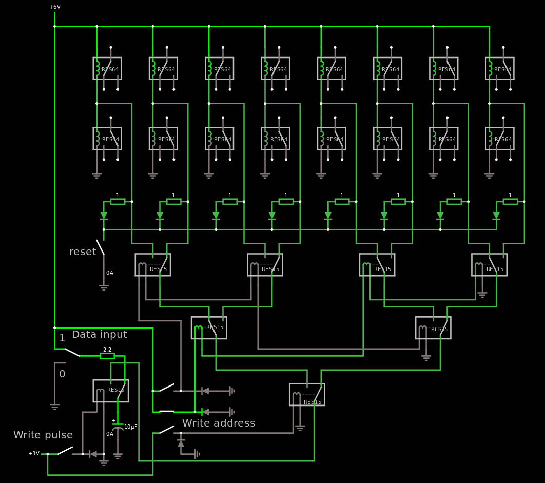
More (virtual) relays
06/29/2021 at 00:49 • 0 commentsI use circuitjs a lot and I just noticed that it now handles relays. After a great exchange with its author, the relays are now more configurable and can simulate hysteresis !
During the tests, it didn't take long to design a bitslice with the 8 registers and the write circuits:
![]()
Having drawings and sketches is nice but making the circuit work is priceless ! Thank you Paul !
Temporary link: https://tinyurl.com/yh8b8ue4
With this many parts, the simulation runs quite slowly. It took minutes to overwrite the 2 leftmost bits but it works as expected !
Adding the read logic is pretty easy at this point but the simulation will be slower.
-
A tale of Flip-Flops
08/23/2020 at 02:42 • 0 commentsThe log 120. TAP v.2 introduced the basic feature of the new circuit : the same counter is used for both phases (in and out) of the communication cycle. This means that it can't use a "normal" counter with its RESET pin and the circuit has been redesigned with partially asynchronous features. The result is this circuit :
![]()
But in practice, this creates some issues in simulation, both with VHDL and circuitjs. The culprit is the infamous double-NOR2 latch that creates oscillations at the start of the sim when both inputs are cleared.
With circuitjs the oscillation stops after "a while", and I have no idea why :
![]()
But with GHDL the sim stops before it begins because it can't reach a stable initial state.
And now look at this version:
![]()
This one has no inversion so no unstable state and no oscillation. This circuit is less favoured because the AND and OR are "2nd order gates" and each requires an additional inverter. But in CMOS there is an extra trick !
The gate OAN21 (or OA1 in Actel parlance) uses 8 transistors : 6 for the function itself and 2 for the final inverter. One inverter stage is saved thanks to the nested topology :
![]()
Meanwhile, each NOR2 (or NAND2) already takes 4 transistors, for a total of 8 transistors for the flip-flop as well, but with possible oscillations. The choice seems obvious in this case.
There is another difference though : the CLR signal's polarity is negated. Usually it is not a problem because the signal can be be negated in a way or another upstream. In the above example, I simply tied the XOR to the inverted output of the DFF but other solutions exist, such as a XNOR.
And there is also a more direct solution, with the OA21NB gate (or OA1B for Actel) where a little swap trick saves another inverter :
![]()
So the Gray6s unit can be updated.
This raises a big question though. R/S flip-flops are used in other places (such as the Selector) and this "bare metal" construct can't be analysed by my library tools because logical loops are explicitly considered as "zombies". They must be explicitly abstracted and this means I can't just replace the 2×NOR2 with one OA1B and call it a day.
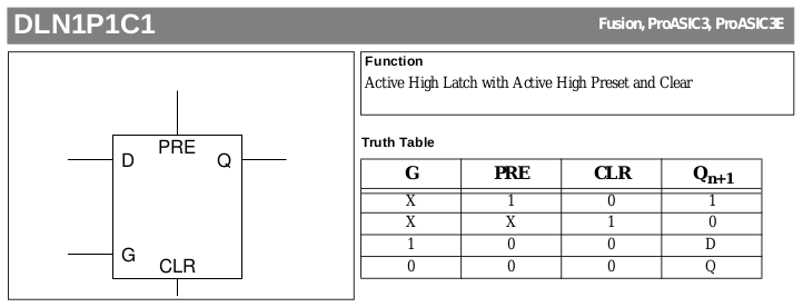
Let's look at the A3P vocabulary : there are no RS FF but it contains these T-latch gates
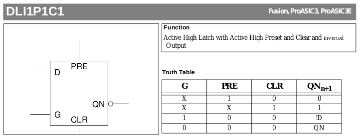
"DLI0    ", "DLI1    ", "DLN0    ", "DLN1    ",
"DLI0C0  ", "DLI1C0  ", "DLN0C0  ", "DLN1C0  ",
"DLI0C1  ", "DLI1C1  ", "DLN0C1  ", "DLN1C1  ",
"DLI0P0  ", "DLI1P0  ", "DLN0P0  ", "DLN1P0  ",
"DLI0P1  ", "DLI1P1  ", "DLN0P1  ", "DLN1P1  ",
"DLI0P1C1", "DLI1P1C1", "DLN0P1C1", "DLN1P1C1"
This looks confusing but there is some kind of logic in this madness. C means Clear and P means Preset, the following digit gives the active level.
- We can already forget the first line because these gates have only a data and clock input.
- Other gates with either C0/C1 or P0/P1 are more useful when a fixed datum is input and the extra pin forces the negative state. There are 16 cases and many degenerate ones...
- The last line with both C and P is interesting because it gives both active-1 Clear and Preset as well as an inverted output (if needed).
There are many ways to build a Set/Reset or Reset/Set gate from these macros but we're not there yet. So let's now enumerate the desirable cases and build a table of the required conditions !
Precedence Set
levelReset
levelMacro
nameMapped to Set 0 0 S0R0 AO1A Set 0 1 S0R1 AO1C Set 1 0 S1R0 AO1, AON21 Set 1 1 S1R1 AO1B, DLI1P1C1, AON21B Reset 0 0 R0S0 OA1A Reset 0 1 R1S0 OA1C Reset 1 0 R0S1 OA1, OAN21 Reset 1 1 R1S1 OA1B, DLN1P1C1, OAN21B The precedence is given by the gate that drives the output (AND for Reset, OR for Set). Conveniently the wsclib013 library also provides the reciprocal gates AON21 and AON21B so 4 combinations are directly available in ASIC (if the B or a2 input is fed from the output).
Other cases could be built from the inverting versions (AOIxx, OAIxx, exercise left to the needy user).
This is cool but this is still not the end of the story because I still can't analyse these constructs. One way is to reuse the existing sequential gates and coerce them into behaving as RS FF.
Looking at the A3P latches, let's focus on DLN1P1C1 and forget about the D and G inputs (let's pretend they're tied to 0).
![]()
CLR has precedence over PRE and this is equivalent to the newly defined R1S1 macro.
DLN0P1C1 and DLI0P1C1 are irrelevant at this level because this does only affect the polarity of the G input.
Then you have DLI1P1C1 which is the same, but with negated output : the functions of PRE and CLR are swapped so the renamed/equivalent macro gives precedence to PRE, equal to the S1R1 macro. Look at the truth table and see by yourself :
![]()
However, due to how the A3P fabric works, DLI1P1C1 is the exact same macro as DLN1P1C1 but the inputs of all the drains of Q are inverted, instead of changing the active level of the Q output. The gate is defined anyway and it's good to know it. But the fundamental problem is not solved.
So what is the real problem anyway ?
The #VHDL library for gate-level verification is meant to help with DFT and in particular ATPG (Automatic Test Pattern Generation). This is possible when the ATPG system can establish the role of all the gates and nets but so far, only boolean gates are covered. Sequential gates are still absent because there is no sufficient theoretical framework to handle that, and that's where the "real problem" arises. In the end, we want to know
- the logic depth between an input port and an output port
- if/how one net can be affected by the input ports and affect the output ports (is a given net observable and controllable).
So far, I consider treating the DFF gates like 2 sides of a "pseudo-port" such that the remaining logic is treated as a single layer. This is more or less accurate but sufficiently so to be useful and functioning. However the world of logical design is not always a dichotomy between boolean and sequential gates... It is more like a continuum but I have identified 4 major levels :
- pure boolean gates : the typical gates that don't hold any state.
- interlocked gates : like the R/S flip flop, some state is held BUT there is a strong boolean component.
- Transparent latch : Can be a pass-through. Or not. So the data can still be considered as boolean, but it may not be so. The latching control input is not a boolean signal however, a new type appears !
- The DFF can not pass through so it could be considered as a non-boolean gate. The clock is a special type of signal (just like the "enable" for conditional storing) but the optional Clear and Preset signals are pass-through and could be considered boolean !
This little panorama gives a rough idea of the complexity of the whole situation. Usually, digital design tools only care for cases 1 and 4 but with cross-clock-domain designs (such as the TAP), this is far from enough.
Going through the "sequential spectrum" allows one to find distinctive features that require special handling. Signals can be classed depending on the ((almost) direct) traversal of the gate (and holding a value is less significant).
- The input signal directly affects the output : it's boolean. This applies to the T-laches (G, D) and also the CLR and PRE inputs of other gates.
- The input signal does not affect the output at this clock cycle : it's purely sequential. CLK and D inputs of DFF apply and can be treated as output ports, while the Q output is treated as an input port.
So each gate can have various attributes and signal types, it's not a gate-only thing (for example DNF1 only has CLK, D and Q ports and is purely sequential, while DFN1P1C1 is mixed because PRE and CLR are pass-through).
The above dichotomy would work in many cases but does not help with the interlocked gates. For the RS flip-flops, the loopback net(s) create a timing paradox, an endless loop that should be avoided, right ?
These backwards nets need to be tested, of course, and can't be ignored. However their immediate effect should not break the design: they are detected and the associated gates are flagged as "zombies". For the DUT to work, these backwards nets must be labelled, which should not be automatic (you can't trust a computer to take the right decisions, do you ?)
So some nets must be explicitly flagged, but VHDL can't allow this (at least in a practical way because the backwards-going net might also be used downstream). The other solution is to flag the input port(s) of the gate(s) that receive(s) backwards data, to prevent the gate from being flagged as a "zombie" and warn the ATPG that some data storage (or maybe oscillation ?) is going on and it's not an error.
It could be handled by adding another "generic" property to each gate (off by default) as is already the case to prevent the test of certain "impossible input combinations" (the generic(exclude: std_logic_vector); that is already used with other gates).
Another more explicit system would be a "virtual time-travelling component" that would synthesise as a wire but handle the loopback in a graceful way, separating the "forward going" net from the "backwards" one. Depth checking would be disabled for the output net of this "loop" component (or its depth would be -1 ?)
So far the jury is still out, the idea is fresh and there could be more options. But soon, more meta-macro-gates will appear, that will help the design of the YGREC8 :-)
After a night sleeping on the subject, the appropriate solution seems to be the "time traveller" component, which should be discussed on the appropriate page :-) And the new RS FF macros are being integrated into the relevant TAP units.
-
TAP pins
08/22/2020 at 23:03 • 0 commentsLet's now talk about the physical interface to the TAP :-)
As already mentioned, this TAP is designed to
- interface directly to a SPI master interface
- require as few pins as possible
- be as simple as possible so the host SW can do all the smart stuff
The typical application uses something like the Raspberry Pi and a half-duplex link with 3 signal wires :
- /WR input selects the data direction (0: write, 1 read from the core)
- Dat : multiplexed serial data in and out signal
- CLK input
The debug system could also access the /RESET pin but this should not be necessary.
/WR, CLK and Dat should have a weak pull-down resistor to prevent any spurious activity when the debugger is not connected.
However the state at these pins could be sampled by the Y8 during Power-On Reset (P.O.R.) to control the state when /RESET is released.
- /WR should not be high on its own because any unsuspecting device connected to the Dat pin could also be a driver and result in a "driver conflict". Thus /WR high would mean a debugger is actively connected and requesting to take over the pins.
- CLK is also usually low but the counter has "a condition" where the synchroniser oscillates during initialisation. Oscillations are removed when CLK is high at startup and it has no noticeable effect on the initialisation sequence.
- Dat should be weakly pulled to 0 because you never know what state would be output when /WR goes high, and a string of 0s is/will be a command for internal TAP reset.
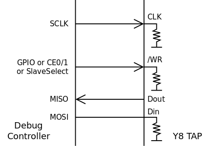
The TAP interface could be implemented in a familiar 4-wires way, as a traditional SPI slave :
![]()
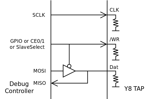
But since Din and Dout are not active simultaneously, a little tristate buffer circuit can save one pin on the TAP's side :
![]()
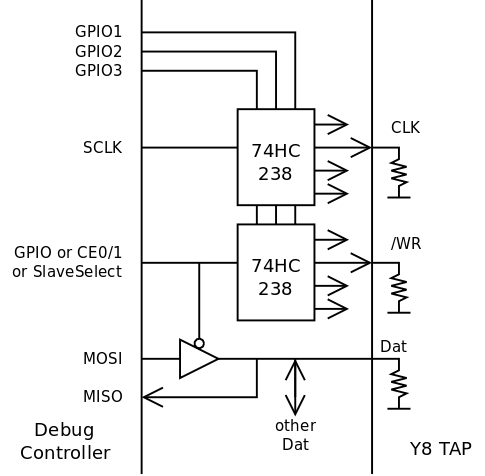
Ideally, with a microcontroller for example, the /WR signal is driven by a GPIO pin. However the Raspberry Pi has "some latency" (around one microsecond in some cases) which could be saved with another trick : use both SPI slave select pins, yet use only one CE pin. This also helps when dealing with the proper polarity, since /WR is active on both levels but Slave Select is usually active low.
Multiple TAPs could be accessed with the same port because the interface requires both /WR and CLK to work. If one of them, or both, is disabled (with a demultiplexer, 74HC238 or 239 as in the example below), commands can not be interpreted.
![]()
If /WR can go high for one TAP only, then the other TAPs will float their Dat pin, which implements the desired multiplexing. If CLK is not demultiplexed as in the above example, make sure to start all the new communications with a blank byte, which ensures that all the other TAPs will not interpret the data as valid commands.
-
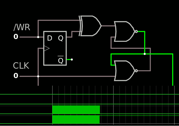
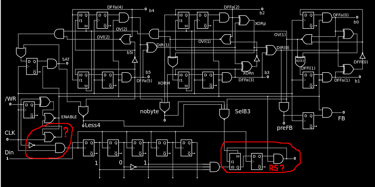
TAP v.2's selector
08/17/2020 at 16:33 • 0 commentsYou might remember the Selector unit from the log 114. The TAP selector: 19 Flip-Flops ! Of course these gates were used and shared but that looks a bit excessive... Using a "prefix approach" lets me reuse the gates so one set of 5 DFF is enough to store the group select prefix and the unit-specific command.
Once the "Group Select Prefix" is received, it must be decoded. As with the first version, only codes 001 to 110 are decoded so there is an expansion rate of 2 : going from 3 input bits to 6 output bits. It would then make sense to latch the 3 encoded bits but there are other considerations : if only 2 or 3 units are implemented, it doesn't make a difference. For now I favour the approach where the decoded signal is latched, so it could be located close to, or inside the addressed unit.
But logically, the new Selector unit has inputs from the pins and the Gray6s counter, and outputs a latched "Group Select Prefix" vector with a desired width. I tried to test the circuit with Falstad's circuitjs and saw that I couldn't go far without having the whole Gray6s circuit where I could tap in some already existing signals. The test circuit is quite large (and I must use minified links now) but only because of the Gray6s unit :-)
![]()
I succeeded to turn the selected output ON but some questions remain, as seen as the red-encircled areas.
- On the left : the original circuit expected the clock to go low before /WR changes.
- On the right : can this circuit be reduced to a simpler Set/Reset circuit ? (There are some spurious signals that seem to prevent it)
Anyway it is looking smaller than the first Selector and the decoding gates can be easily reused by the addressed units :-)
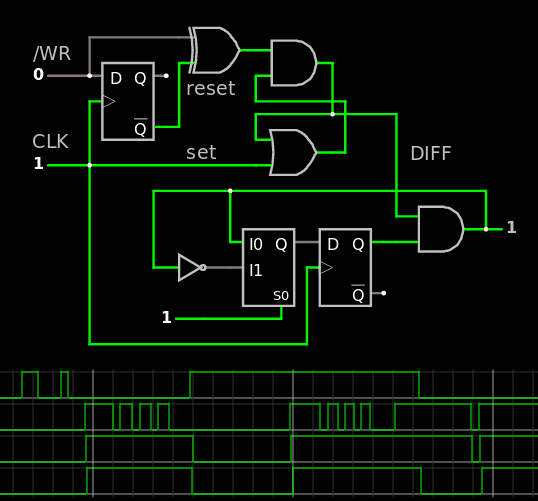
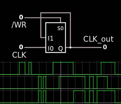
Well the problem on the left is solved with a MUX2 / T-latch :-)
![]()
There is no need to connect the clock gate to the above Set/Reset latch.
However : this works ONLY if the clock level after and before the /WR change is the same. This still creates a spurious spike when
- CLK = 0 when /WR goes up and
- CLK = 1 when /WR goes down
But this should not happen, right ?
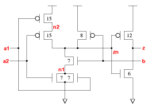
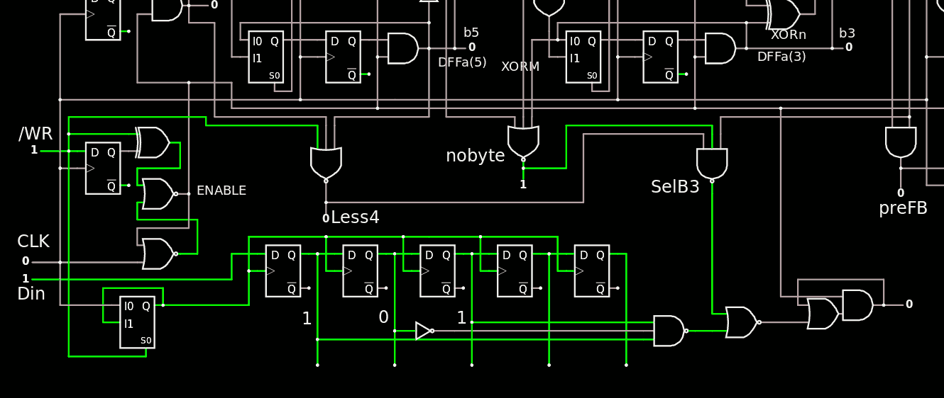
The new circuit is here :-)
![]()
This helps to define the modifications required for the Gray6s unit :
- Less4 is now NOR3 that counts /WR as input.
- nobyte and SelB3 can be done externally, in the Selector
- SelB3 needs OV(1)
The output latch can indeed be reduced to a Set/Reset cell, here made with a OA1 but a pair of NOR2 could work as well. The rationale for this choice :
- it takes much less silicon
- The spurious pulse comes after the first normal pulse due to an interaction with the clock. If the latch is already set, there is no harm to set it again one cycle later (it doesn't change the state).
The state change as soon as the 3rd clock pulse is received, which could create issues in the other units. I'm testing if/how I can activate it on the falling edge of CLK.
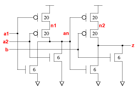
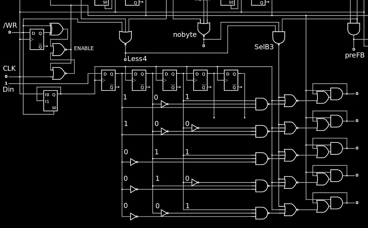
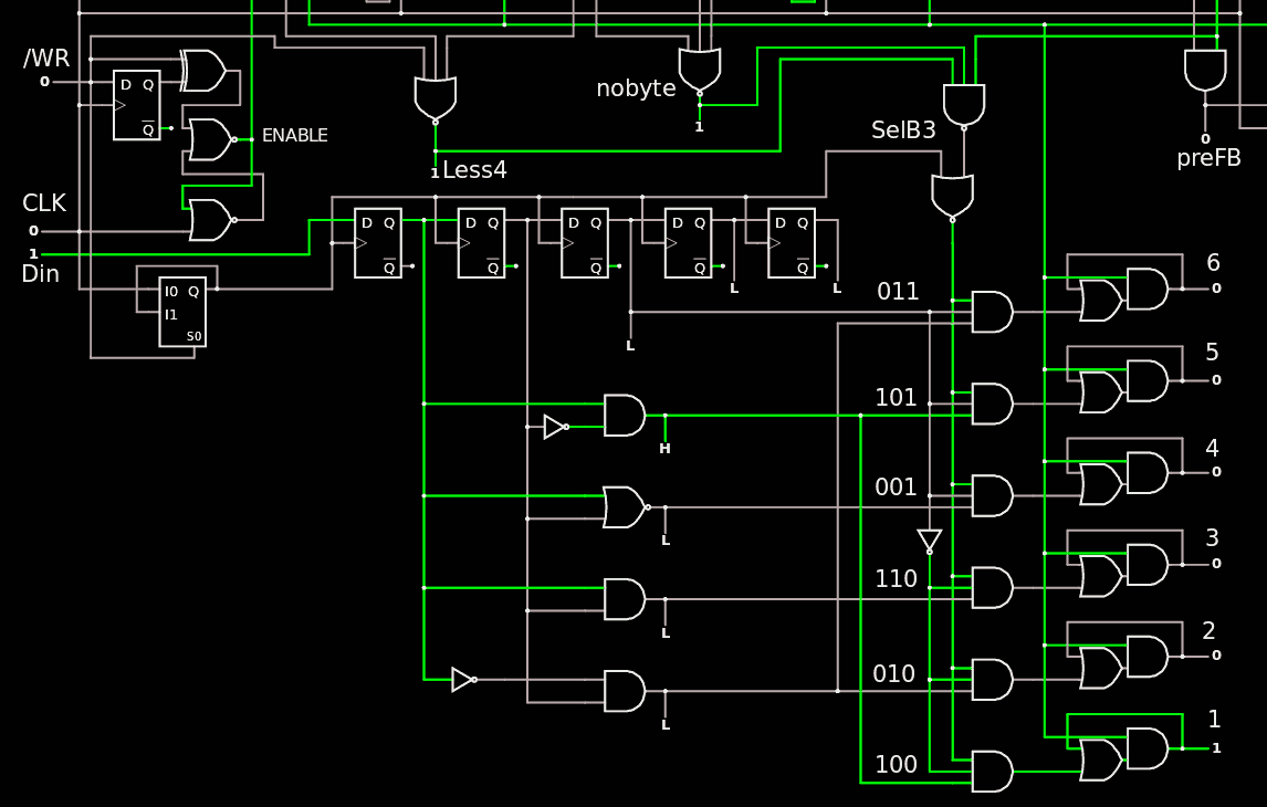
And here is the Selector with 5 decoded outputs:
![]()
I know I should have factored the decoder's inverters but it's only an illustration that will be refined.
The duplicated NOR3s with SelB3 and CLK should also get a special treatment to reduce the logic and wiring... So there it is !
![]()
The predecoders are also shared with the rest of the TAP to reduce efforts&complexity. These predecoders are also provided for the other bits of the shift register :-)
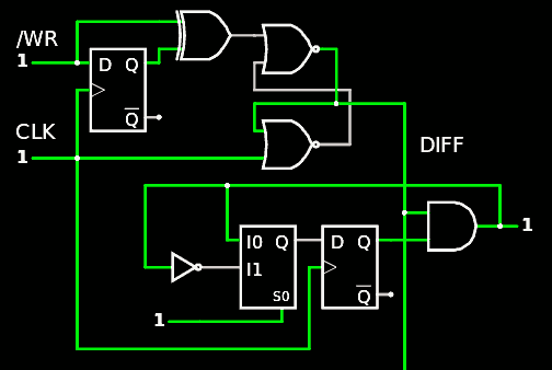
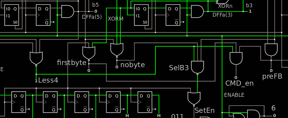
Speaking of predecoders : another signal that the other circuits will need is when the first byte is shifted in. I modified the existing circuit by adding 2 gates :
![]()
- "firstbyte" is much like nobyte, but instead of checking 3 Gray bits for '0' (which gives a granularity of 4 counts), the DFFa(2) signal is traded for the CLK input to remove the glitch further downstream (and the granularity is 8 counts).
- CMD_en goes high at the end of the 7th clock pulse, ready for being latched in the 8th pulse. It's a bit like FB (Full Byte) but restricted to the first byte only.
preFB is glitchy because it uses logic results from the counter, but it seems that gating the signal with /CLK solves the problem, the DFF for FB could even disappear one day.
At this point, the circuit looks complete and just waits to be implemented in VHDL.
The selector is now provided in the latest archive, starting with YGREC8_VHDL.20200821.tgz. The unit uses a Generic to enable/disable the implementation of individual selected outputs. By default, all the outputs are enabled :
entity Selector is
  generic( implemented : SLV6 := "111111" );
If you set one of the bits to '0' then the corresponding output will be tied to '0' and no latch is implemented.
This should save a few gates... but no such elimination is provided for the 8 predecoder outputs, the dangling outputs and gates will be detected/handled by the synthesiser. -
TAP timing & simulation
08/16/2020 at 01:58 • 0 commentsAs I rebuild the tests for the latest archive YGREC8_VHDL.20200815.tgz, I find a weird behaviour : the last test of the TAP takes what feels like ages to complete.
The usual procedure, after you decompress the archive, is to run the script ./test_units.sh which will ensure everything is OK (tools, files, regression tests and so on). Self-tests are run, one after another, and I don't use a makefile because it tends to obfuscate things. If I wanted to use all the CPU I could parallelise some parts but for now, I don't run ALL the possible tests, often because they are pointless. There are various versions of the same unit and some are not relevant.
For the TAP, I have the "behavioural" version of the Gray6s counter, and the "tiles" version, both work as intended. The test.sh script works nicely, with behavioural completing in no time, while the Tiles takes 1/2s. But it appears that the Tiles version has some unexpected side-effects when used along with the MUX64 and I can't find why. test_readback takes more than 7s to complete ! After tweaking the order of the initialisation lines, that time is halved but the 3.5s is still too much for doing nothing (I tried to find where/how that time was wasted but it still eludes me). I want the whole script to run fast and smoothly, I'm not running an exhaustive test but thorough enough that one can be confident to explore the rest of the options with a working system.
For now the solution is to run the piso_order and test_readback programs with the behavioural counter. I suspect is could be an obscure VHDL thing with the "discrete" R/S latch of the resynch circuit but I can't be sure yet. Anyway the purpose is to run decently fast simulations and the Tiles version is not required at that point, as long as the behaviour matches with the higher-level description.
Apparently the gates library adds some significant overhead when the number of gates increases. The TAP simulates faster when the "simple" build is chosen, without the fancy stats stuff. However regeneration of the library would take almost as much time as running the system with its about 100 gates. A tiles-less version is chosen for the TAP's first tests, but other options are possible (commented out in the scripts). Behavioural simulation is fast enough anyway in the first checks. More detailed simulations can be performed later...
The archive is re-uploaded and the ./test_units.sh script completes in < 11s.
Oh, it just dawns on me that I could compile the "simple" gates library in a different directory, with the same name, and select the version by the directory path... This is now explained in Abnormal initialisation time and workaround. and the archive is updated with the new "dual style" system.
-
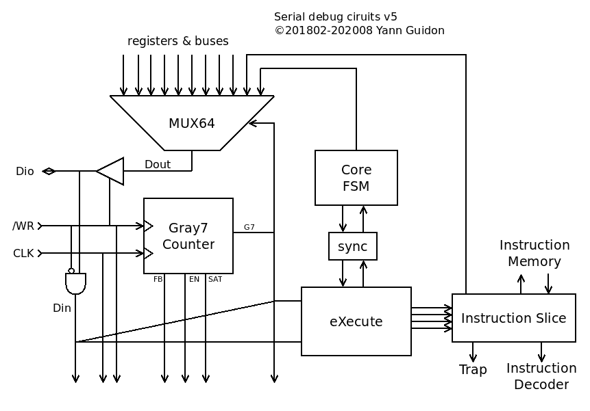
TAP v.2 : where it's going
08/13/2020 at 22:16 • 0 commentsThe MUX64 is unchanged, the Gray7s circuit is redesigned, the Instruction Slice remains quite the same... The new general diagram shows that we're left with the redesign of the Execute module :
![]()
There is one gotcha though, compared to the behaviour of the previous versions :
If you read the MUX beyond the 64 bits, the Gray counter will loop and wrap around in the reverse direction, before going in the forward direction again, and so on...
I might have to reduce the size again because it seeeeeems I might not use the whole counter range. See below.
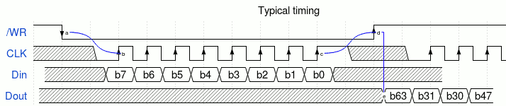
The timing diagrams have not changed much because the TAP is still driven by the same type of devices (microcontrollers or SBC with a hardwired byte-wide SPI master). So sending a single byte will look like this :
![]()
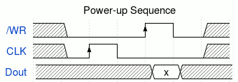
There is a required "little dance" on /WR and CLK after powerup to ensure that the internal state is determined:
![]()
Strobe CLK up-down (at least once, could be 8 times), then /WR up-down, and you can read and write as expected (just make sure the serial pin is not driven when /WR is up). Other registers will need to be initialised as well, as there is no real "reset" pin.
There is a significant change on the horizon though. I'd like to use a prefix (byte ?) to also simplify the Selector (it has disappeared on the main diagram). The first byte could be a "short command" to the FSM for example, but for longer messages it also steers the data to the right shift register. Some clock resynch is required for these sub-clocks to prevent a spurious rising edge but I think I found a solution tonight.
Furthermore I have split the first byte into the prefix and the command. This saves some gates because the prefix is latched first, then the command can reuse the same DFF gates. With 3 bits of prefix and 5 bits of command, only 5 bits need to be stored by the new "selector". Furthermore, since decoding logic is shared between the prefix and the command, some further gates could potentially be saved. Then, only 6 units can be selected because prefixes 000 and 111 are reserved (it can reuse the same decoding logic as the previous selector). To save further on gates, each unit will contain its own selector latch and logic.
I like it because that is one internal state fewer to init and/or keep in mind when programming. The command is the state and the system needs fewer cycles to get into a nominal functioning state (and it uses fewer gates). It is less resilient though and the commands must be carefully documented because there is no ASCII mnemonic.
The other benefit is with the timing : the serial interface generates the pulses that were hard to come up with the first version. The /WR pulse can be used to strobe transparent latches, for example.
As a result : most of the commands that were defined so far in 116. TAP summary & protocol will be either 1 or 3 bytes long...
-
Updated Gray Counter
08/10/2020 at 10:42 • 0 comments20200814 : back to 6 bits because it looks unlikely I'll use 16 byte-long messages. Look at this circuit :-)
![]() Total count : 39 gates :-)
Total count : 39 gates :-)
The rest of this log is still very informative.
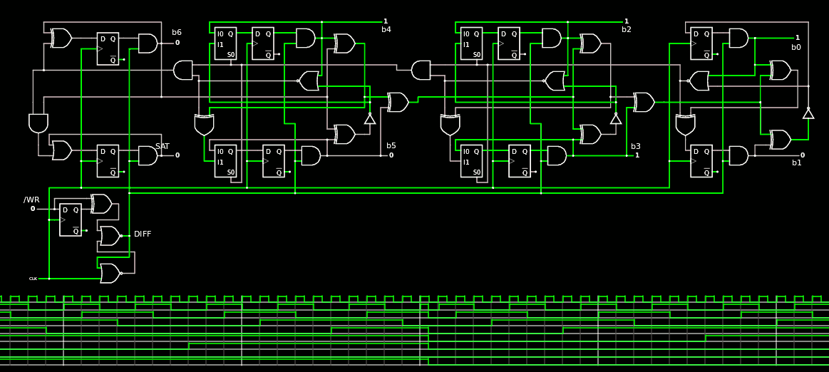
With the new TAP v.2, I reconsider the detailed design of the whole circuit and merge the two counters into one. This means that I must remove the /RESET input of the DFFs, which in fact are not desired because basic ASIC gates don't have one anyway. I must also increase the size of the counter a bit and add a SAT output (plus some pre-decoded bits such as FB or NULL). With these enhancements, the same counter can drive both the MUX tree for Dout and the other decoders for Din.
The log 109. Gray counter explains all the details of the construction of a modular/cascaded Gray counter, check it out if you haven't seen already !
From there the first step is to expand the counter to 7 bits and add a saturation bit :
![]()
Then the DFF with RESET must be substituted with a DFF and a AND2 gate.
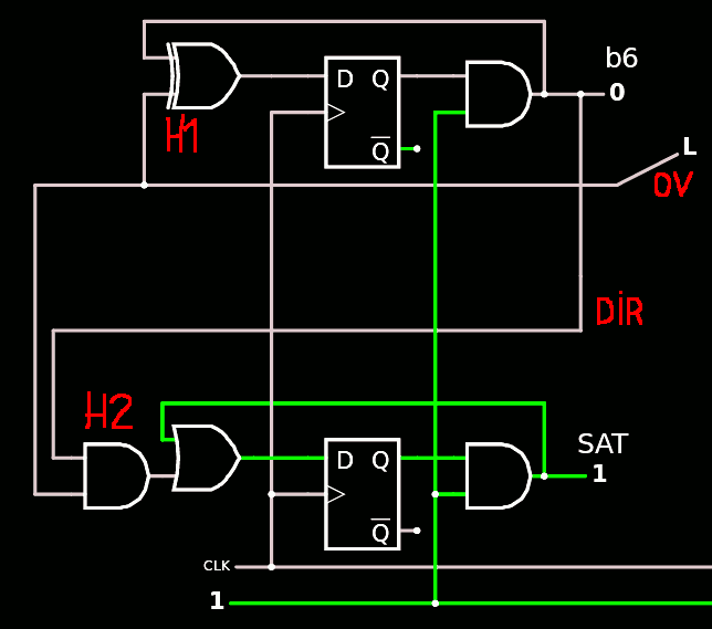
Let's start with the MSB : SAT and B6
![]()
The funny thing is that the AND and XOR gates can be understood as a half adder, because B6 is toggled every time OV is on, and SAT is enabled when both OV and DIR are on. This could help simplify a bit if a "half adder" gate is available in the ASIC PDK but H2 seems best merged with the following OR2.
The DFFs have no RESET input as expected. The SAT output could even drop the DFF but it would be ON during cycle 127 and not 128, thus reducing the usefulness of the whole circuit. The DFF delays the flag by one cycle and allows the use of the full 16 counts.
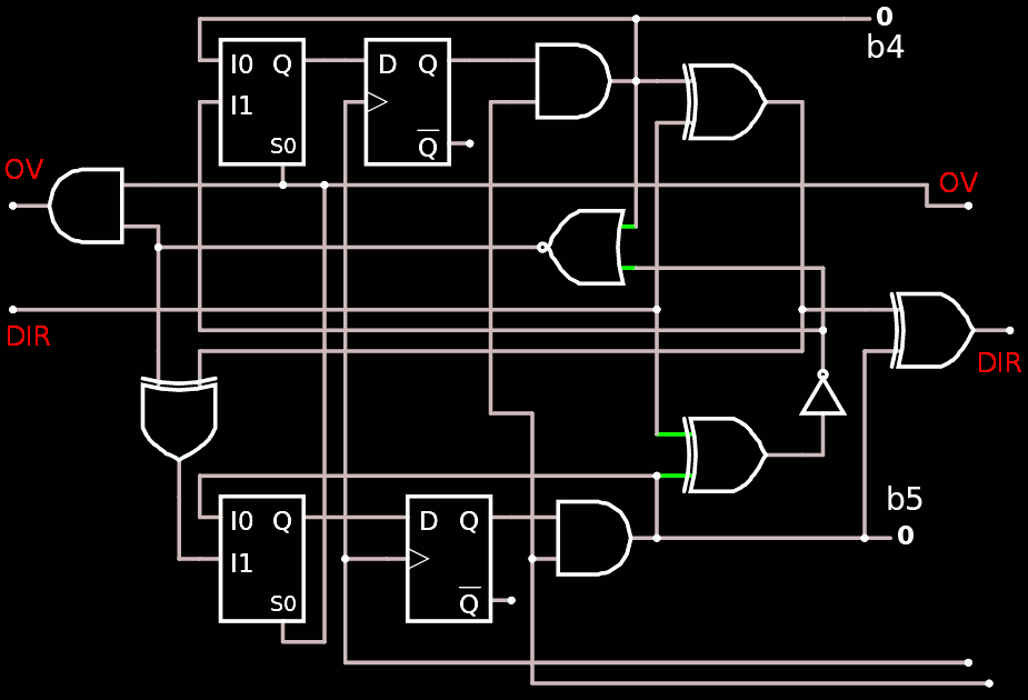
The middle module(s) have nothing specific to be said about...
![]()
I simply added the AND2 at the output of the DFF and removed the RESET pin.
Same for the the LSB : it's a simple adaptation.
![]()
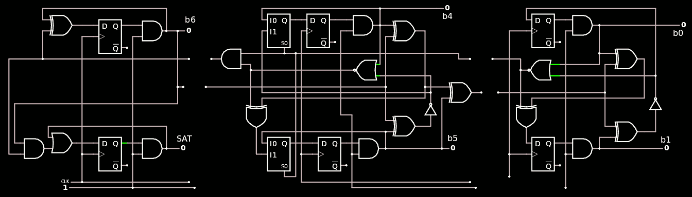
.The modules are gathered in this link so they can be reused and adapted later for other eventual purposes.
![]()
I hope it will be useful to others ;-)
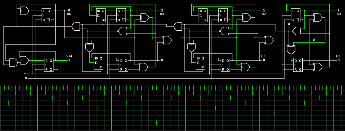
The whole counter is there : it looks like such a mess that I'm glad it's modular ;-)
![]()
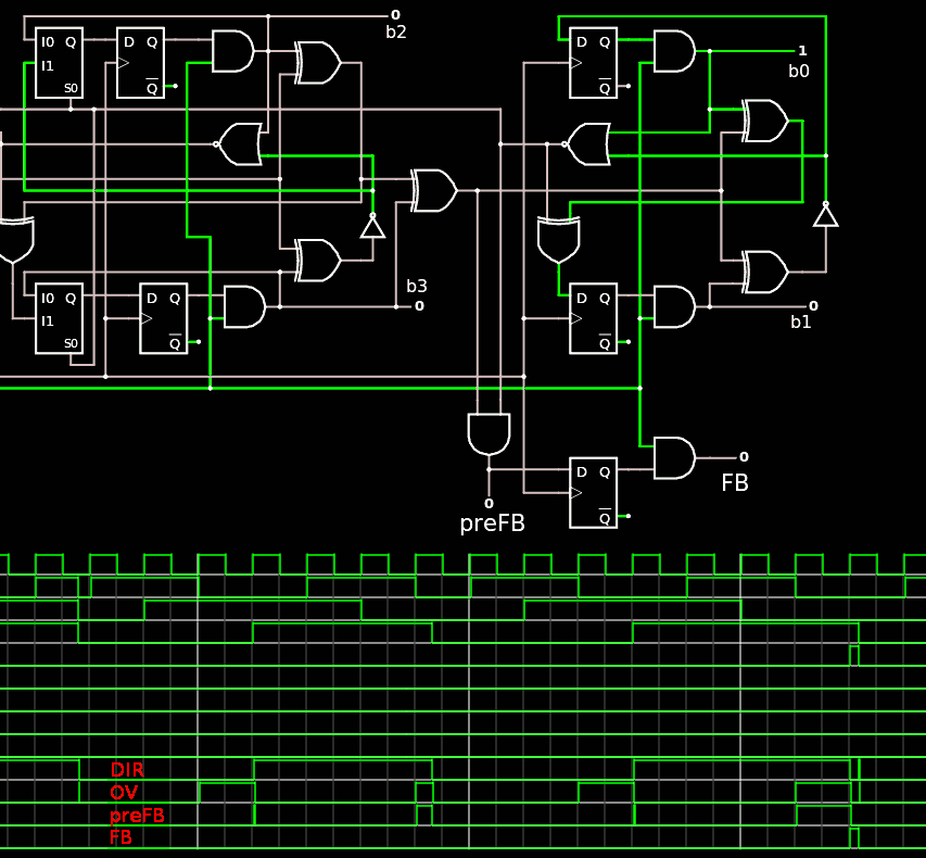
And it works nicely when driven by the circuit described in 120. TAP v.2 :
![]()
(of course this is not the typical way to use it but it works anyway)
Now, writing it in VHDL is another story.
Stay tuned !
Oh I almost forgot ! The earlier Counter unit has a FB output that is needed in most of the other circuits. It turns out it's quite easy to generate but not as I originally thought : just AND the DIR and OV signals from the LSB module. The circuitjs diagram shows that the result of the AND is a bit glitchy on the the 4th (mod 8) cycle but the DFF resynchs the signal. The AND result is provided as a partially decoded signal preFB, in case it's needed in other places...
![]()
The trick is to ensure that the /WR toggles work as intended, there is a AND after the DFF, and there is no need to AND before because the OV and DIR signals are already ANDed anyway.
It is also useful to provide pre-decoded flags for when the byte count is low. I added the Less4 output signal that is a NOR3 of SAT, b6 and b5, such that it is 1 when the count is less than 4 bytes.
As the circuit has grown beyond the linking capacity of the site, I saved the description as Gray7s-fb-l4.cjs in the archive.
The whole thing is pretty large, now...
VHDL implementation was not difficult, thanks to the previous version and all the planning that is logged on these pages. It compiled (almost) right away and thanks to rigorous checks during the writing, only one small numbering mistake remained and was easily spotted.
Total count : 46 gates (incl. resynch, sat, FB), while the earlier Counter was 31 and Gray6 was 21 (and with special DFF with Reset). So the net gain is 6 gates but there are 16 DFF that have been replaced with a smaller version without RESET.
This new version will greatly ease the design of the other modules !
YGREC8
A byte-wide stripped-down version of the YGREC16 architecture
 Total count : 39 gates :-)