
cyborg ring
cordwood + smt + jewelry + blinkies + zinc-air batteries
cordwood + smt + jewelry + blinkies + zinc-air batteries
To make the experience fit your profile, pick a username and tell us what interests you.
We found and based on your interests.

OSHWA certification. Yay! The cyborg ring is US000141. That means as of this posting, I'm responsible for around 4% of all certified projects. Wait that is bad, it means more people should get certified. Certify your projects! Don't let Open Source Hardware become a stupid marketing term (or at least, continue to be that).
I also did a major documentation update which can be seen in the README.md in the GitHub repo, available here. The repo now contains all the instructions of record, and will likely be the thing I update first whenever I get around to a fresh cyborg ring iteration. But I'll keep this project updated too, so don't worry.
I did a live stream of a ring build and it went pretty well. Certainly better than the first recording I made. Just shy of two hours with shitty audio:
Also, I made ten kits.
they are simple but hopefully well instructioned enough for an intermediate solderer to enjoy over the course of an evening or two. also they come with lots of extra parts.
goodbye kits. enjoy the protection offered by my favorite corrugated box:
more on this development in a few weeks...
A few folks on Twitter ordered PCBs and wanted to start a cyborg ring build slack channel, so I obliged. Link to join, if you are interested: https://join.slack.com/t/cyborg-ring/shared_invite/enQtNDAwNDA0MDE1OTcyLWUwMWFlMjE0MmZmYjY5NDkwNzc4MDA1ZTMyYzc4MmFkMjNjY2EwYTA2ZGZkZDA2NzQ4YzYwNzhmODBkNDBjN2M
I think this invite expires in a month, so.. if you read this afterwards, remind me to update it!
@F0cks built a cyborg ring and proposed to his girlfriend! Awesome. He made a few excellent improvements (sized down to 6.5-7, programming pads on one side, etc); check out his excellent build log here: https://blog.f0cks.net/projects/Cyborg-ring/
Also I added a programming diagram to the repo, as the previous text description was difficult to follow. And wrong.
CC-BY-SA 4.0
https://github.com/zakqwy/cyborg_ring
Someday this will end up on Crowd Supply as a kit, but if you're impatient.. have fun!
I assembled the new ring version some time ago but didn't get a chance to putz with the programming until now. Gross, programming. But yay, yellow LEDs:
Used a pin change interrupt on the button to wake up the t85; previously, resting current draw ("resting") was nearly a milliamp which nuked the batteries in a few days. Now down in the microamp range, which should make Zn-air life the limiting factor (4-6 weeks depending on use):
Note that I kept the pogo rig together but soldered wires on for iterative programming. It's fussy to repeatedly align.
Reinforcement wires worked like a charm. I took a few traces dangerously close to the PCB edge which bit me this time, but nothing a few jumpers couldn't fix:
The ring also has a bit of conformal coating, and I used the largest spring tabs from the previous order (A108284CTs). Assuming the ring doesn't break in the next week, I'll wear it to Teardown.
I intend to tackle a few problems with this revision. None of the changes are huge, and thankfully didn't require any rework in Inkscape and only needed a bit of re-routing.
I used OSHpark's 0.8mm / 2oz double-sided service to save a bit of width on the ring. When the boards arrived, they were nicely routed but required a decent bit of clean-up with a file as mousebites aren't nice to fingers:
Note the holes on each positive battery contact; these are Zn-air cells, so the vents should be exposed to the atmosphere.
The circuit includes two board-to-board jumpers along with four high-resistance structural resistors, all made from standard 0805 components. I pre-assembled these on a heat-resistant surface (in this case, my PTFE-jawed Stickvise):
Easiest method here is to carefully align the two components with tweezers...
... dab a tiny bit of flux at the junction...
.... and touch the junction with a tinned iron tip.
Done!
Once I had the 0805 jumpers sorted, I started soldering the vertical components onto the switch side of the ring. I followed my standard SMT soldering procedure here: a drop of flux on the pad...
... careful alignment with tweezers...
... and a touch with a tinned iron tip.
The same procedure works for the QFN ATtiny, too, although the iron 'touch' turns into more of a 'scrub'. If this doesn't make sense, I made a QFN hand-soldering video a few months ago that explains the concept a bit better. Note that in both cases, holding the part near the bottom helps a lot to ensure the component is square. Practice makes perfect...
Examination through the loupe ensures we've got a good fillet (not yet defluxed...):
The rest of the parts go on in a similar manner. The LEDs live on either side of an 0508 stubby resistor, so I soldered these onto each side before mating the halves, as shown in this picture from an earlier log:
[keen observers will notice that this is a different copy of the board with the QFN rotated 90 degrees. This was wrong, and I actually had to rework this component after the two halves of the ring were assembled. Yes, solder braid can work miracles.]
Since the batteries are a bit under 4mm tall -- more like 3.3mm, give or take -- I used a set of tiny spring tabs to fill the gap:
[yes, I didn't really plan the PCB footprint around these tabs, so they hang over a bit. And the QFN definitely needs to be straightened out. Soldering under the camera is a pain.]
These worked for a time, but eventually the batteries fell out; the tabs plastically deformed after a few insertions and eventually broke. During one of the periodic tab tightenings I attempted over the course of a few days, I pried a bit too hard and the back of the ring actually broke. It seems that I need to treat 0805 resistor stacks like unreinforced concrete columns -- not so great in tension, as the caps tend to pop off:
Fortunately none of the pads were damaged, so I replaced the resistor jumpers with lengths of wire. I used tiny scraps of self-adhesive conductive RF gasket for the batteries, which seems to work but still doesn't seem ideal:
Just popped in a new set of batteries, so I'll wear the repaired ring for a bit and see if any other weaknesses pop up. I'm starting to make a list of improvements for the next rev which I'll share next time, as this log is already long enough.
I started this project by measuring my wedding ring. I like its form factor and it fits well enough, and the wide curved stone on the top seemed like a nice element to replace with LEDs:
That got me in the ballpark; my fingers are all different sizes and I figured the PCB edge wouldn't be nearly as accommodating as a smooth gold band, so I decided on a ~19.5mm opening. After creating initial footprints in KiCad and pulling them into Inkscape (via *.svg export), I putzed about for a few hours and came up with a reasonable PCB outline:
I then imported the outline as a *.dxf file (twice) into KiCad and got the two halves aligned on the same grid: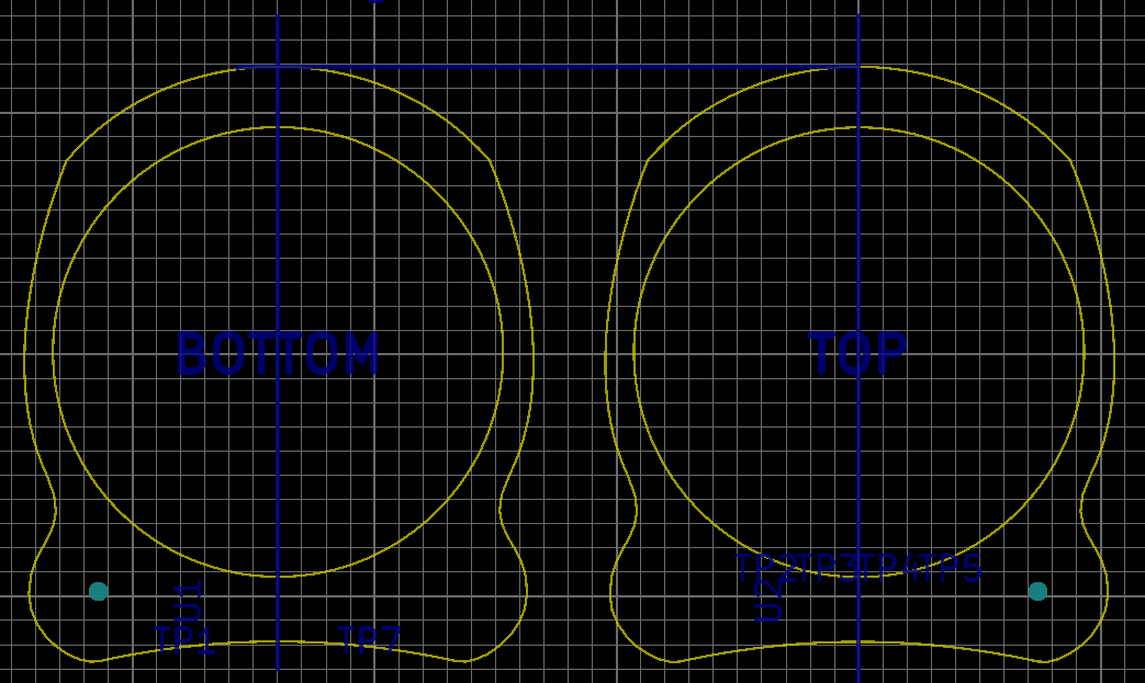
Note that I added the specs to the PCB comment layer, and manually named each LED footprint to its appropriate net. Then I deleted all the originally imported LED footprints. Probably a simpler way to do this, but it worked for me.
Routing was straightforward. I arranged the Charlieplexed LEDs in such a way that I minimized vias and was able to run the four signal lines as four pours around the skinny part of the ring, which avoided awkward jointed traces: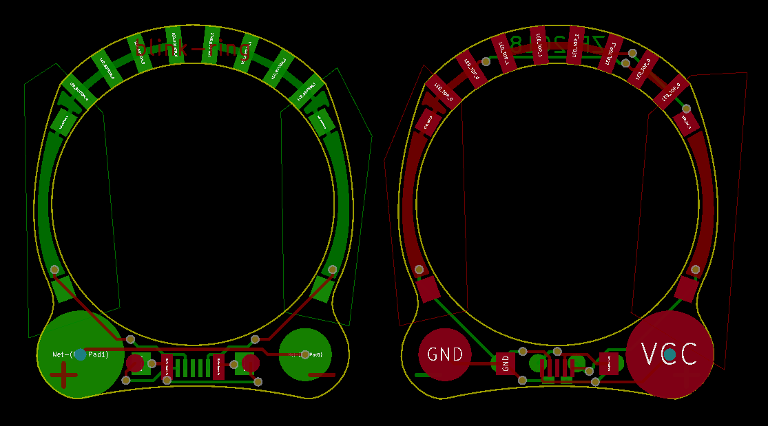
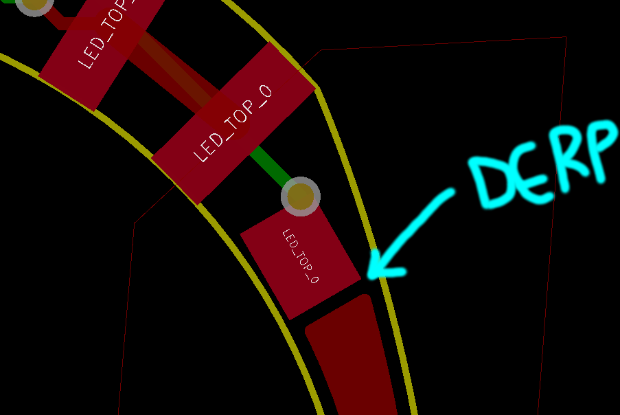
I build weird PCBs. Most include copper- and mask-layer graphics, and they often feature complex routed outlines beyond the normal 'this-needs-to-fit-in-an-enclosure'. My tools of choice are Inkscape and KiCad, following a clunky but effective workflow:
I usually lead with KiCad: throw together a preliminary schematic, make footprints as needed, pull them into Pcbnew, right-click-global-spread-and-place, and export the grid of components into Inkscape. Starting this way ensures the graphical work gets done at scale; most graphics and board outline decisions are bounded by component sizes so it's nice to have this in place up front. Then I put together a first pass at graphics and board outline, export to KiCad, and start high-level routing. Inevitably this results in numerous minor changes that drive the iterative loop until I get sick of the process and send the board out for fabrication. It's no PCBmodE, but I don't think I could live without real-time DRC and push-and-shove routing.
Fundamentally, this process doesn't change with SMT cordwood construction beyond a few extra considerations.
First, cordwood design is confusing. You are designing a circuit in which every component is split in half on the schematic, so it's a lot to keep track of. Between this project and #Splinter, I have found that (a) drawing the schematic (and potentially testing the circuit) in a conventional manner is helpful; and (b) keeping components precisely laid out across from their counterparts is a necessity:
As you can see, I've made a few schematic symbols that are specifically designed to minimize confusion; they even look like they're supposed to interlock across the gap. Remember, KiCad knows how to handle routing on a single PCB, but you have to keep track of routing between the two boards. Note that this means you can't just drop GND and VCC labels everywhere -- keep them on one side if you use them at all!
This layout strategy extends to the part placement process, since opposing boards must be inverted and perfectly aligned. The strategy here is to sort parts into two piles, flip half to the back side, align the two PCB outlines to the same grid, and use comment-layer lines and visual cues to ensure component alignment:
Second, component selection is driven by component length in addition to the usual myriad of other characteristics that one finds via parametric search. SMT cordwood doesn't have the luxury of component leads to absorb small differences between components; everything has to be pretty much spot-on. In the case of this project (and #Splinter for that matter), the key gap of 4mm is based on the dimension of the QFN version of the ATtiny85. Why this part?
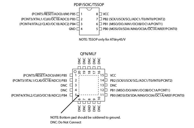
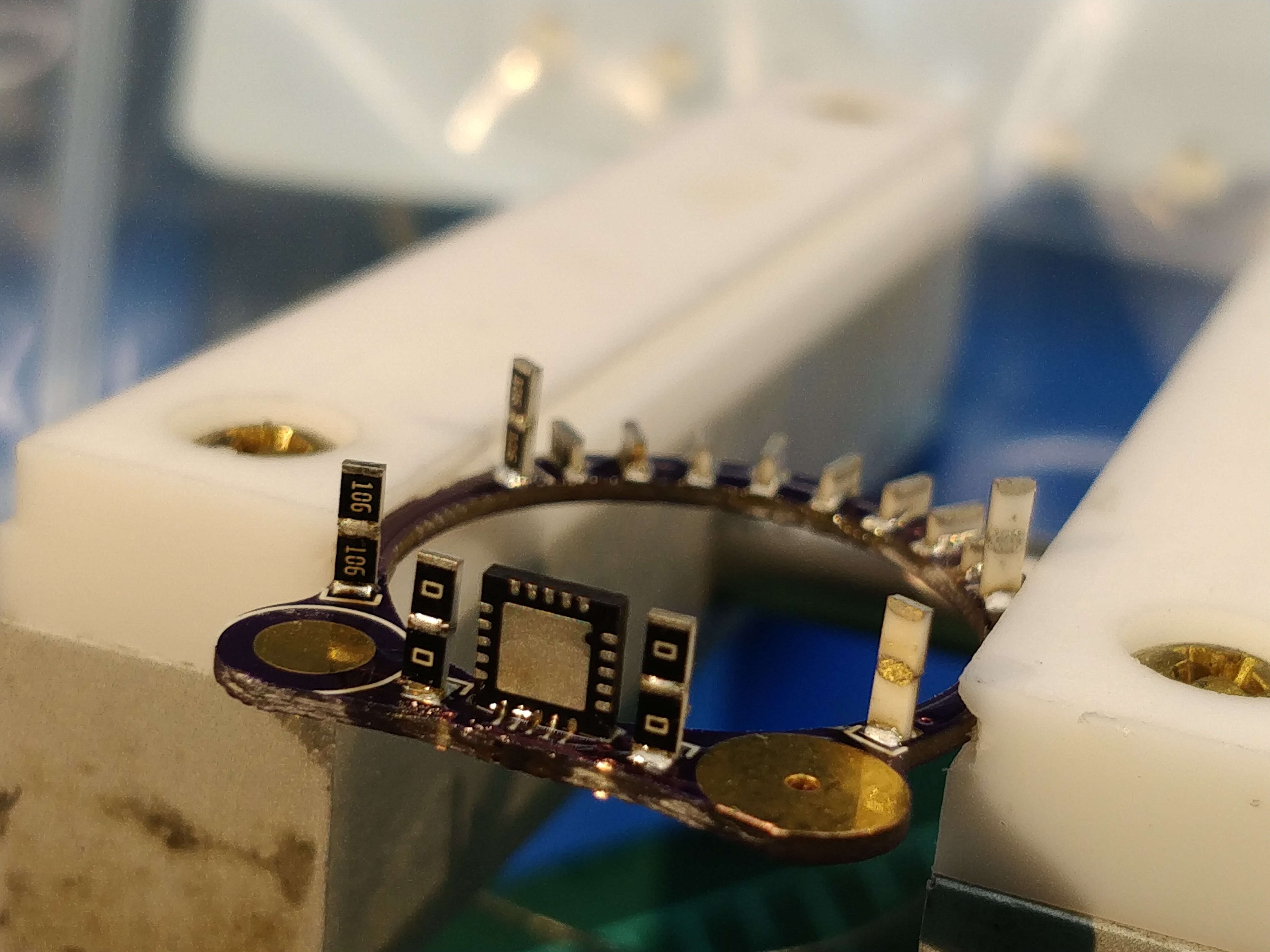 [above, the resistors marked '106' are 10M each -- effectively insulators for the part of the circuit they short out. They are purely structural elements. The resistors marked '0', on the other hand, are jumpers and quite important for circuit operation!]
Once this chip was selected, I worked backwards using Digi-Key's parametric search and a good bit of datasheet examination. I'll put up a Page later on with an updated list, but for now my 4mm span cordwood compatibility guide looks something like this:
Create an account to leave a comment. Already have an account? Log In.
This really is some black magic... "purely structural" SMD resistors? You've added more details since I looked last and I'm still just flabbergasted by this hardware art.
If you want to bring it back around to its "bare metal" roots, call it Ring0
Become a member to follow this project and never miss any updates
By using our website and services, you expressly agree to the placement of our performance, functionality, and advertising cookies. Learn More
 Linus Dillon
 MakersBox
 Jarrett
 Jean Simonet
Nice work Zach!