MagicWolfi
-
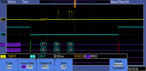
MISO crosstalk
11/23/2015 at 00:08 • 0 commentsI am currently testdriving a Tek scope and found one issue on the board that was undetected so far.
The MISO signal picks up some cross-talk from the parallel SCK lock line during the cycle that writes the register address to the MAX11300 chip. This is how it looks on the scope.
![]()
The amplitude of the signal is to low to cause any glitches, but a different board with a different flavor of Arduino might look differently.
A pull-down resistor should take care of this issue and finally there is a good reason for the next revision.
-
Informational: MAX11301
08/16/2015 at 02:49 • 0 commentsMaxim's PIXI, 20-Port Programmable Mixed-Signal I/O with 12-Bit ADC, 12-Bit DAC, Analog Switches, and GPIO is now available with I2C interface instead of SPI.
PN is MAX11301.
I imagine data transfer will be much slower, but if you don't have the pins available, I2C is always a solution.
-
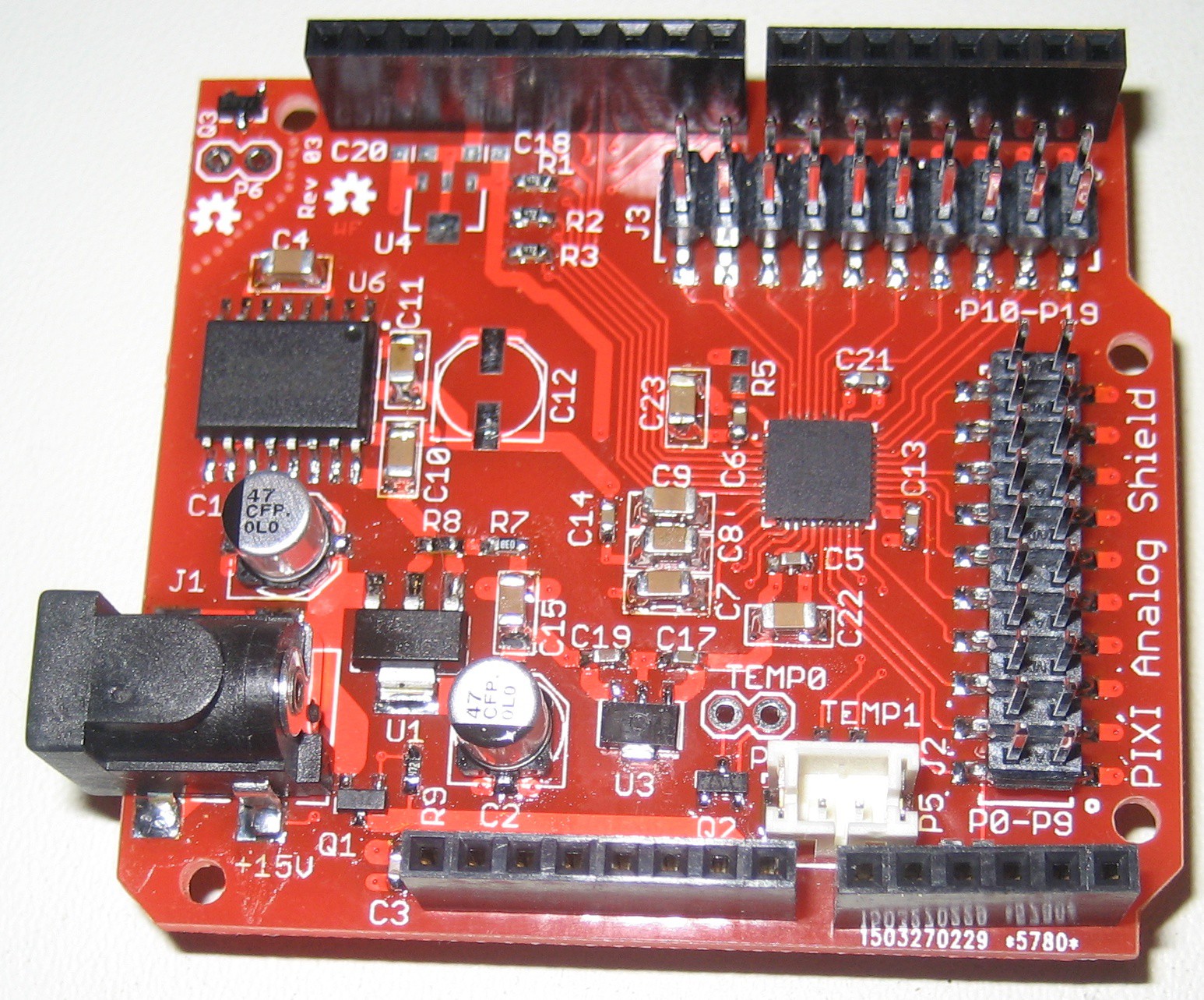
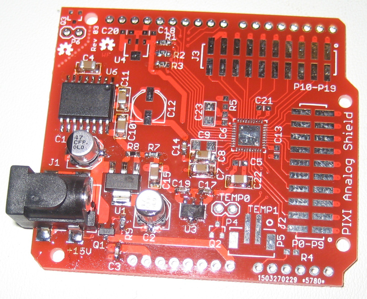
Rev 03 power up
05/10/2015 at 15:33 • 0 commentsThe 1st board of rev 03 is assembled and works very well so far. SPI communication is established, the internal and on-board external temperature sensor are operational. And most important, the analog inputs and outputs seem to be happy. At least the ADC DAC settings with 0v to +10V voltage range.
![]()
With the internal voltage reference and my crappy multimeter looping back the DAC value into a ADC, I see the following results:
DAC ADC U[V] 0x0000 0x0000 -0.0039 0x0400 0x03FB 2.507 0x0800 0x07FE 5.02 0x0B00 0x0BFE 7.52 0x0FFF 0x0FE8 9.98 Looks decent, I am just not sure yet what happens at the top end of the range.
-
Rev 03 Power rails are high...
05/03/2015 at 05:31 • 0 comments... and low. Just finished assembly of all components required for the power rails and they look beautiful, without load that is.
![]()
AVDD: +5.07V
AVDDIO: +12.31V
AVSSIO: -12.29V
-
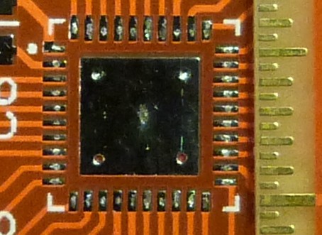
PCB rev 03 arrived
04/26/2015 at 05:24 • 0 commentsFinally the boards from Dirty PCB arrived and they are looking sharp. I got 10 pieces and the quality is outstanding. All copper features are crisp and the silkscreen is excellent. Even 1mm text size and 0.1mm line thickness is readable. The HASL finish adds just enough material to be able to tack on components without extra solder. For full pictures see the project gallery. And here is a closeup of the QFN-48 footprint. The EEVBLOG uRuler comes in very handy to show the 0.5mm pitch.
![]()
Can't wait until Monday when I have access to the Mantis microscope to place the MAX11300. The rest of the components is just as easy as my standard saying: "If I can see it, I can solder it".
And who finds the mistake in the silkscreen, look at the full board? Sometimes I feel that a correct silkscreen is the hardest part of a layout. There is always one designator facing the wrong direction (not this time - it is much worse).
-
Rev 03
03/27/2015 at 03:51 • 0 commentsThe next revision of the board is ordered and it is Rev 03, not Rev 02 as usual. This time the design is done in Eagle and the board house of choice is really cheap and dirty (here). We'll see how the quality turns out. Design files will be released when the board turns out error free and I found the time learn how to speak github or so.
![]()
Now the question is, what to do in the ~3 weeks until the boards arrive. Get some programming done or start a new project? I don't have a good idea for the Hackaday price 2015 yet.
PS: Rev 02 was a board with all known issues fixed done in KiCAD, which never made it to a board house.
-
External or Internal Voltage Reference, that is the question?
02/28/2015 at 20:57 • 0 comments3 different configurations are tested to see if the internal reference voltage is good enough or if an external one is needed for best accuracy.
For the test a LM4040-2.5 0.1% tolerance was used.
Reference ADC INT REF ADC EXT REF DAC REF Internal 2.4999V 0 2.4964V External - 10 Ohm resistors 2.5033V 2.4991V 2.4991V External - no resistors 2.5033V 2.4991V 2.4991V Now I output a set of values through a DAC and read the voltage level back with an ADC and compare input and output values. The voltage range for ADC and DAC are set to 0v to +10V
Internal reference:
DAC ADC U [V] 0x0000 0x000 -0.0070 0x0400 0x0401 2.4920 0x0800 0x0801 4.9919 0x0C00 0x0C00 7.4886 0x0FFF 0x0FED 9.9282 External reference, input and output with series 10 Ohm resistor:
Circuit for the external reference:
![]()
DAC ADC U [V] 0x0000 0x000 -0.0041 0x0400 0x03FB 2.4920 0x0800 0x07FE 4.9983 0x0C00 0x0BFE 7.4976 0x0FFF 0x0FE6 9.9361 External reference, input and output shorted without series Ohm resistor:
DAC ADC U [V] 0x0000 0x000 -0.0042 0x0400 0x03FD 2.4970 0x0800 0x07FE 4.9992 0x0C00 0x0C00 7.4990 0x0FFF 0x0FE9 9.9381 The DAC does not seem to be capable of driving all the way up to the maximum value. More measurements are needed.
Returned ADC values seem to be best with the internal reference. The external reference without series resistors has the best voltage measurements, but adding cost to the BOM. Lower voltage measurements seem to be shifted 4-12mV (2-5 LSBs) to the negative side.
-
So many LSBs
02/22/2015 at 23:48 • 0 commentsNext step in the test process was to loop back a DAC value into an ADC and compare the result to the output value. The read back ADC value was in the order of 24 LSBs lower than the original output value. For example at a voltage range 0-10V a DAC value of 0x400 resulted into a output voltage of 2.4920V but the ADC value was always around 0x3e8.
Tests with an external voltage reference and a linear regulator instead of the switched capacitor voltage converter for the negative rail did not show any improvement.
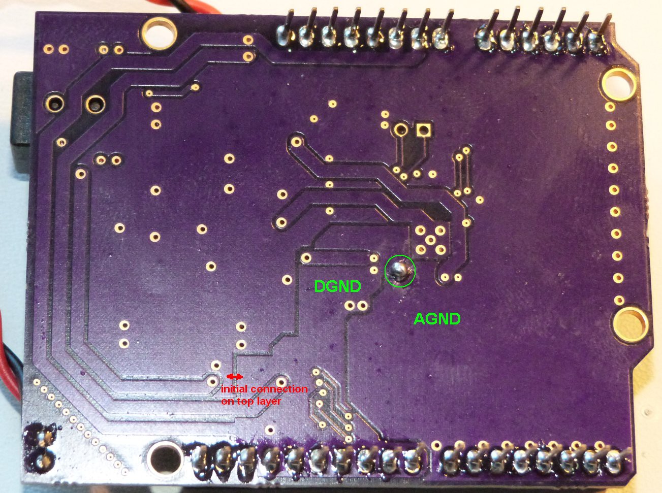
The issue revealed itself while monitoring the analog voltage rails and SPI communication was active. During every SPI data transfer, a lot of noise was visible on the analog side. This pointed to a less than optimal GND connection point between analog and digital GND. Tying the 2 GNDs together direct under the analog IC instead of the original place close to the optional digital regulator, solved the issue.
![]()
Now the loopback test shows a variation of 2-3 LSBs, which is a very good improvement.
-
Communication established
02/22/2015 at 00:34 • 0 commentsHooking the shield up to an Arduino and establishing communication went totally smooth until I tried to read the DEVID register. My code
const int slaveSelectPin = 10;

// Config SPI interface
pinMode (slaveSelectPin, OUTPUT);
 digitalWrite(slaveSelectPin,HIGH);
SPI.begin();
SPI.setClockDivider(SPI_CLOCK_DIV2);
SPI.setDataMode(SPI_MODE0);
SPI.setBitOrder(MSBFIRST) ;

    word result = 0;
    byte read1 = 0;
    byte read2 = 0;
  digitalWrite(slaveSelectPin,LOW);
  //  send the address and return value via SPI:
  SPI.transfer( (address << 0x01) | PIXI_READ );
  read1 = SPI.transfer(0x00);
  read2 = SPI.transfer(0x00);

digitalWrite(slaveSelectPin,HIGH);

  result = (read1 << 8) + read2;
returned 0x0424 instead of 0x0024 as specified in the datasheet.The only reason I can think of is, that my engineering samples have a different ID to make them distinguishable from production parts.Everything else seems to work as documented and after setting up 1 DAC and 1 ADC I was able to output and read back analog voltages in 4096 steps in voltage ranges from 0V to +2.5V and 0V to 10V.
Overall a promissing start.
-
Initial Power Up
02/21/2015 at 05:47 • 0 commentsI found 2 wrong schematic symbols, which got fixed on the rev 01 board with 1 deadbug IC and one that was not required for regular operation. The interested observer will find those fixes in the image of the board.
PIXI Analog Shield
An Arduino Shield using the Maxim MAX11300 for 20 Programmable Mixed-Signal I/O with 12-Bit ADC, 12-Bit DAC, Analog Switches, and GPIO