I spent an all-nighter making a simulator for the card, which can load the schematic from KiCad, then spent an egregious amount of time in the sim making the card work. As promised last log, I will show a bit more on the simulator:
For those that prefer reading over watching, I'll do some brief explanation of the simulator, then go over the card itself.
About the Simulator
The simulator loads the KiCad PCB file, constructing a netlist and list of components. There's a (small) component library, which has a simulation model for each component type. The simulator schedules chip updates based on each IC's propagation delay, so the simulator should be largely accurate from a timing perspective too.
The simulator has some handy features for graphics devices particularly, for example, a VGA display simulator. In the picture, there is a white dot on the VGA display - that is the position of the electron beam at this particular tick. The sim was definitely engineered to my particular use case. Well, I'm pleased with it and hope to use it in projects in the future. Now I can know if a board will work before I order it.
The simulator uses a lot of bit manipulation, and for this reason, it does not at all support analog signals at this time. It's great for simulating logic chips and RAM - or really any ICs that are digital.
I also connected the simulator to my Teensy 4.1, so I could run a simulation with the software in the loop. You can see that in the video up there as well.
Oh, what is that I hear? You could have just used an existing simulator!! Really? Huh, I guess that didn't seem fun enough, well, too late now anyway. Well, here's the source code, if it is wanted: https://git.nuclaer-servers.com/Nuclaer/kicad-logic-simulator But also, I don't think an existing simulator would have all these features I wanted, and honestly, building this sim didn't take *that* long. I'm really amazed I did it as quickly as I did; I would have expected it to take at least twice as long to write a program like this.
I love MUXes
I replaced many of the logic gates with MUXes, as it is a lot easier to understand what the logic is doing, and the logic is just so much more flexible this way. I got the idea from LUTs in FPGAs, which work in a very similar fashion. The MUXes can accept quite a lot of inputs if you're creative, since you have select lines, enable lines, and inputs - this can afford you a lot more logic per chip than logic gates.
3 of the 4 MUXes my deisgn uses nowChanging the RAM
I think I went over this in my last log but I don't remember; well, I needed to change the RAM ICs. The speeds on this board are extremely fast, with a maximum of a 32Mhz pixel clock. I needed RAM that could read/write in less than 30ns for the card to have the whole display written fast enough from the Teensy (or whatever other device). Hopefully I did my math right because I already made the card use different RAM ICs, and these are blazing fast, at 25ns. Unfortunately, this dramatically reduces the maximum graphics memory, which is now 128K (up to 262144 pixels). These numbers are halved if you use hardware double buffering. This limits the highest resolutions to 640x400, or 540x480, for example. This bothers me, so maybe I'll have to make an upgraded card in the future.
I think the design will work, based on the simulation, so I'm finally uploading the schematics after this log is posted. This time I'll add the component libraries and such too, so there will be less issues a few years from now in KiCad 11.0, or whatever will be brewing by then.
Let's take inventory of my mistakes, so you can hold them against me:
The address connections A16 and A17 from the VRAM to the uPD7220 were not set up completely right, causing a strange monitor flicker in mixed mode, and lack of memory access if the software didn't have a special setup
VRAM control lines were not generated correctly
The VRAM was not fast enough to do what I had in mind. I thought I checked this and I knew the timing was close, so I must have done my math wrong.
Probably something else I forgot
I thought there might be a minor issue or two with the design, as the design of the VRAM access is very ambitious - accessing two words per cycle using careful timing, then switching what device controls the memory every other cycle. Yes, a lot can go wrong. But what I didn't expect, is that so much would go wrong. I practically have to re-design more than half the board. Well, that is more or less what I've been working on.
Here's a video showing what the debugging was like; hopefully the video isn't too chaotic:
At some point I realized that I couldn't figure this all out by messing with the hardware directly - there were just too many things wrong with the board. The breadboard was losing me both signal integrity and voltage - the board ran at less than 4.3v. I needed a simulator. Well, I wrote one. It works decently well, loads my schematics straight from KiCad, can show me the VGA video output, and has a few other random features. Here's the source on my personal gitlab server, and here is a picture of it:
It is VERY alpha, and the library of components is incredibly limited. It has bugs and the UI can crash sometimes. That being said, the simulation itself does not seem to have any problems. It does just one thing extremely well: it simulates the card I'm working on. With some relatively small upgrades it could probably be used to simulate a wide variety of digital circuits.
In any case, I've been using this simulator to work on a fixed design. This is still in progress; I'll post one more log when I order the boards, then I can try again when I receive the improved boards. I'll go over my changes to the board in depth on the next log, but basically I've switched the SRAM ICs to 25ns chips so I can get the timing I want, and I've removed most of the logic gates and replaced them with MUXs to make something akin to LUTs - kinda like an FPGA with TTL, except the LUTs are hardwired. Much easier and more reconfigurable than trying to use gates - and in some cases it's actually faster too. Well, until next time. Wish me luck on a fixed design!
KiCad 3D render of my board design:I tried to make the parts of the circuit clearly visible on the board. I also added LEDs, which I typically forget when designing a board. Every board needs blinking lights. Well, I think this board has turned out nicely, at least in the 3D render; it has the clean look I wanted.
Here's the ratsnest and basic layout before I routed it:The board now:This board was a lot easier to route than I expected. Anyway, expect an update in maybe 10 days when I actually assemble it.
I have the schematic finished now. I checked the major critical paths to the VRAM, fining one that was too slow. The VRAM takes up to 55ns from address input to data output, and I have only 62.5ns, so really it is super close. Since the uPD7220 uses an address latching mechanism, I managed to move my address-modifying critical path to before this latching is done. The timing there is much more forgiving. Other than that, I added some pretty LEDs and checked/fixed some of the logic done in the circuit.I may add more decoupling capacitors still, but that isn't a real design change. The capacitors are the only SMD components I'm using.
In total I'm using 32 TTL ICs, two RAM chips, and the uPD7220 of course. Loading it in the PCB editor, it looks smaller than I may have expected, but I don't think I'll feel the same when I receive the finished board - it is significantly bigger than my original uPD7220 card:I think I'll also need to make some minor adjustments to the circuit design so the routing is easier, but these are not really functional changes - things like changing the bit order on registers, or rearranging the allocation of gates from chips.
This schematic is way better organized, and hopefully it will still make sense to me 5 years from now. I've added a ton of features since the last board revision, namely:
The CPU can now directly access the VRAM
I doubled the maximum pixel clock by allowing for uPD7220's wide mode (see last log)
Added support for double buffering
I octupled the maximum VRAM to 512KiB from 32KiB. Now we can have larger resolutions with enough RAM left over to double-buffer
Doing all this added a TON of extra logic, so if you compare the above schematic with the schematic of the previous board, this one has at least twice the components, and is far denser.
I had to add a lot of buffers so that the VRAM bus could be shared. This concerns me because it adds a few tens of nanoseconds to certain datapaths, meanwhile I've doubled the maximum VRAM clock speed to 16Mhz. The VRAM uses 55ns alone, and that doesn't count any of the hardware for uPD7220 memory cycle detection, bus sharing logic, etc. So the next step will include checking my datapaths to make sure all the components process fast enough for my clocks.
Here is some of the new logic for handling the communication from the main processor directly to VRAM:Some of this logic is wrong I think, namely I'm suspicious of the two bottom NAND gates, and I need to add logic for the WAIT line, but this image should give some idea of what the logic is supposed to do. After the main processor writes the lower address byte, the byte-select for the VRAM is reset to zero. Then the processor can write a single byte to the VRAM, which automatically switches the selected byte so the processor can write the other byte. This is done because the VRAM has a 16-bit bus and the processor has an 8-bit bus. Depending on weather the address counting is enabled, the address registers will actually count up to the next word in VRAM, so that the processor can send up to 128KiB of uninterrupted data to VRAM. This is done in-between accesses done by the uPD7220, as the bus is shared, and the uPD7220 gets priority.
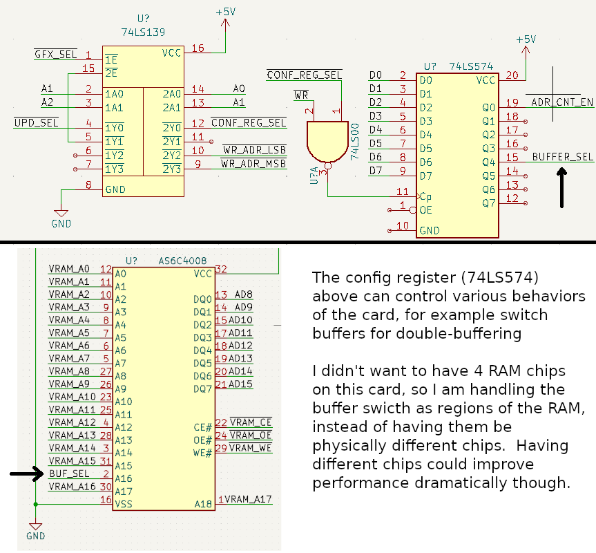
The exact behavior of the board's logic is controlled by a special control register I added:I realize now, looking at this, that I may be able to remove a latch by using A0 for byte select instead of automatically selecting it. Something to think about. Anyway, in the image above you can see that the config register can enable/disable the wide mode logic, control automatic address count, enable or disable double-buffering, to swap buffers, and set A16/A17 for direct VRAM access. The double-buffer enable will make the uPD7220 and processor write to the opposite buffer as the one being displayed, but the buffer still must be manually swapped by the processor.
Anyway, this is where I'm at now. The schematic isn't quite finished, once I finish it and have the board design I'll upload the files to the project.
[edit] bonus: falstad simulation of part of the circuit responsible for loading pixel data from VRAM and clocking it out, which allows wide mode: Simulation
I found part of the datasheet discussing "wide display mode", which tells the uPD7220 to skip an address each time it loads a word to be displayed. Here are the relevant sections of the datasheet:As it turns out, I don't think I can get it to add 4 instead of just adding two as described above; this limits my maximum clock speed to 24Mhz (32Mhz on the faster Z7220), so the maximum resolution would be limited by this. On the other hand, the uPD7220 supports interlacing, so I might be able to push out a higher resolution that way. Without interlacing under this config, I can't even get to 640x480, but with interlacing I can get at least to 720x480. I'll have to play with the settings.
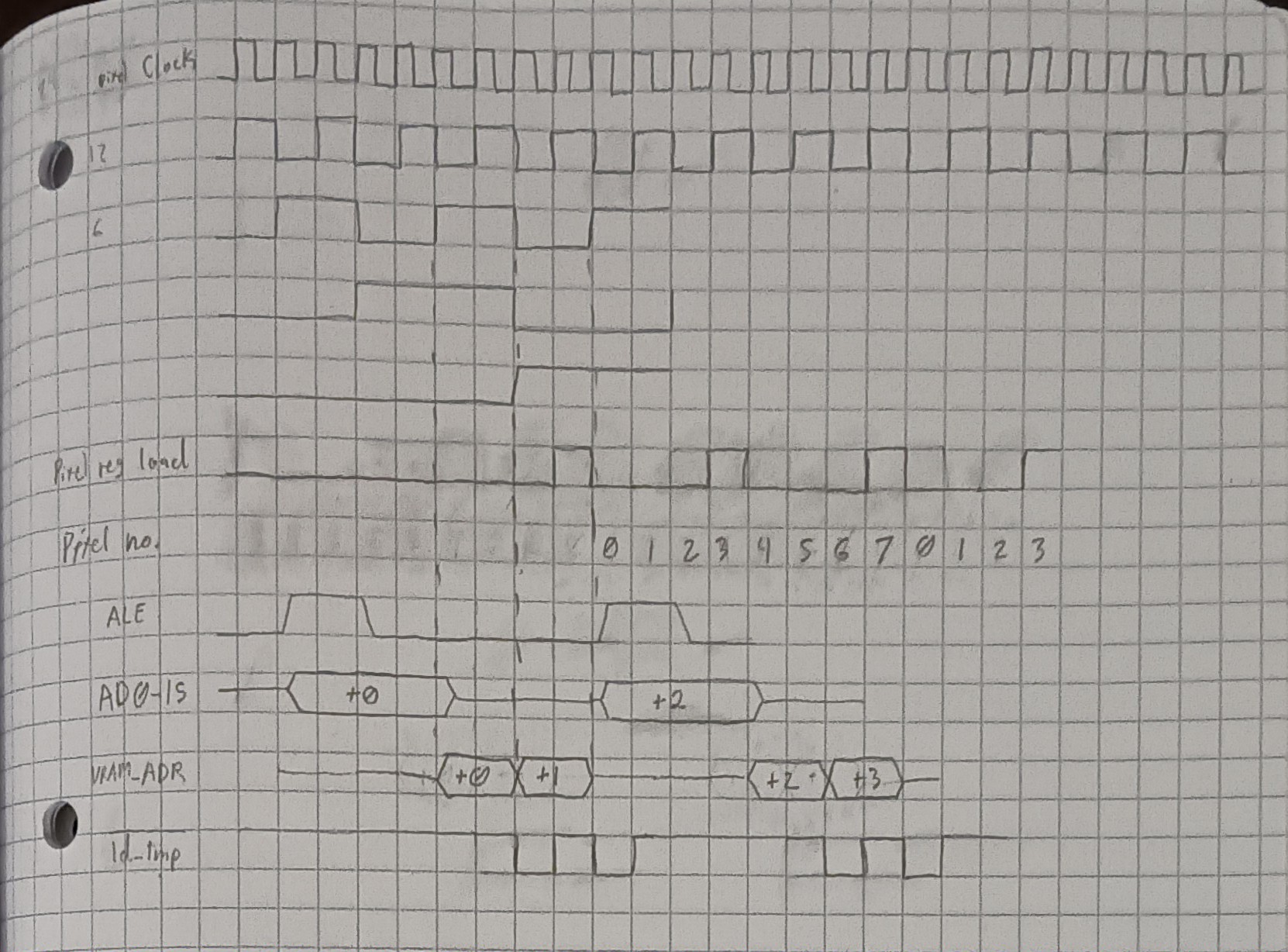
I'll need to add a 16-bit register to handle this, since I don't have a real 32-bit bus to load color data from: I still need to add the logic to generate LD_PIX_TMP, which requires detection of the uPD7220's memory cycles. The waveforms should look something like this:
The clock at the top is the pixel clock, the fastest it can do is 4x the max GDC clock (so 24Mhz for uPD7220, 32Mhz for certain Z7220 variants). The third clock from the top is the GDC clock. The color shift registers load every fourth pixel clock, shown on the 6th signal down from the top. Each GDC memory cycle we will now be loading 8 pixels instead of just 4, so you see the pixel number reflect this. Once the address is latched, we can load two words in succession, at twice the GDC clock speed. To do this, we use the 16-bit register previously mentioned, which loads twice during this single GDC memory cycle, once for each 16-bit word. The first time it does this, the color shift registers are immediately loaded, thus saving the color data for the first four pixels. This way, the same 16-bit register can be reused to save the next word. The LOAD signal to this register is shown as the active-low signal on the bottom of the image above.
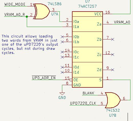
Here's the logic I designed to generate this waveform: As a bonus, I'm including a timing diagram from the datasheet so it is easier to find later:This image details the cycles of various uPD7220 memory accesses, and is super useful for designing the memory control logic.
I hadn't looked at this project in a long time, and the other day I was browsing it and noticed several comments asking for the schematics. But hadn't I uploaded schematics? So I double checked the files, found the attached schematic zip, and decided to open it up. Oh geez, what a mess! It had been created with a very old KiCad version compared to today, and I don't think I uploaded the symbol libraries, so the schematics were useless. I can see now why people asked for the schematics!
Very useful indeed. (not)I spent some time the other day cleaning this up, as well as fixing a few hardware bugs related to the color DAC and oscillator. I modified the schematic to match the modifications on my board at home, which works quite well. Here's the schematic now, which I uploaded:A lot better, but still messy.The wires are very messy, consistent with how I made many schematics in highschool. Clearly, this schematic needs to be redone from scratch. Well, if I'm going to redo the schematic and roll a new board, why not make a bunch of improvements too? Well, this is exactly what I've been working on.
Upgrading the board If you saw my log in #Arduino Desktop, then you'll know that I mentioned this project, in that I may want to add it to another Teensy or ESP32 based computer system. A Teensy 4.1 could write a lot of data to VRAM very quickly, which would be great for drawing bitmaps, and in-between the uPD7220 can draw other shapes. In that log I also mentioned double-buffering the uPD7220, so there would effectively be two RAM banks, which could be switched by some command. To my knowledge, the uPD7220 does not support this, so I needed to add the logic myself. I'm still working on the schematic, but here's where we are so far:I'm not a huge fan of the old board's low resolution. I want at least 640x480, if not higher. Adding more memory for this is quite easy, and in the new schematic this is already handled - the hard part is getting the clock speeds high enough. The uPD7220 can clock at 6Mhz, and the current card gets this by dividing it out of a 12Mhz clock. With a Z7220 the clock is a bit higher, 8Mhz and 16Mhz respectively, but this is nowhere near the pixel bandwidth needed for higher resolutions. My solution to this will be to divide the uPD7220's clock one or two times so we can get 24Mhz or 48Mhz pixel clocks on a uPD7220. That should allow us to get way better resolutions: I really hope I'm using this calculator right.The 800x600 resolution in the above image is a good spot, and uses about half of the VRAM, leaving the other half to be used for double buffering. I haven't made this part of the circuit yet, and one big thing I'd need to figure out is how to get the right signals to the VRAM for loading the pixels. I could generate the VRAM's A0 with some logic to load two words out of VRAM each time the uPD thinks it's loading one, but this introduces an issue where the uPD would not be able to draw graphics to half of the pixels. Perhaps there is a way to have the uPD skip a word each pixel load, then simply modify the A0 line to load this way? I don't know yet, I need to consult the datasheet and see how this type of thing was done in the past. I have a feeling they may have used two uPD7220s for this type of thing, but let's see if we can do it without that. The chips are rare, after all, and the Z7220s are even more rare.
Here is the current clock generator circuit for the new board, which should behave exactly the same as the old board; its job is to generate clocks for the board and to control when pixels are loaded into the output buffer: Anyway, I have more stuff to figure out with the board. If any of you have good ideas on the clocks and loading twice the pixels from RAM, let me know :) Hopefully my schematics are prettier and more useful this time; I think they will be.
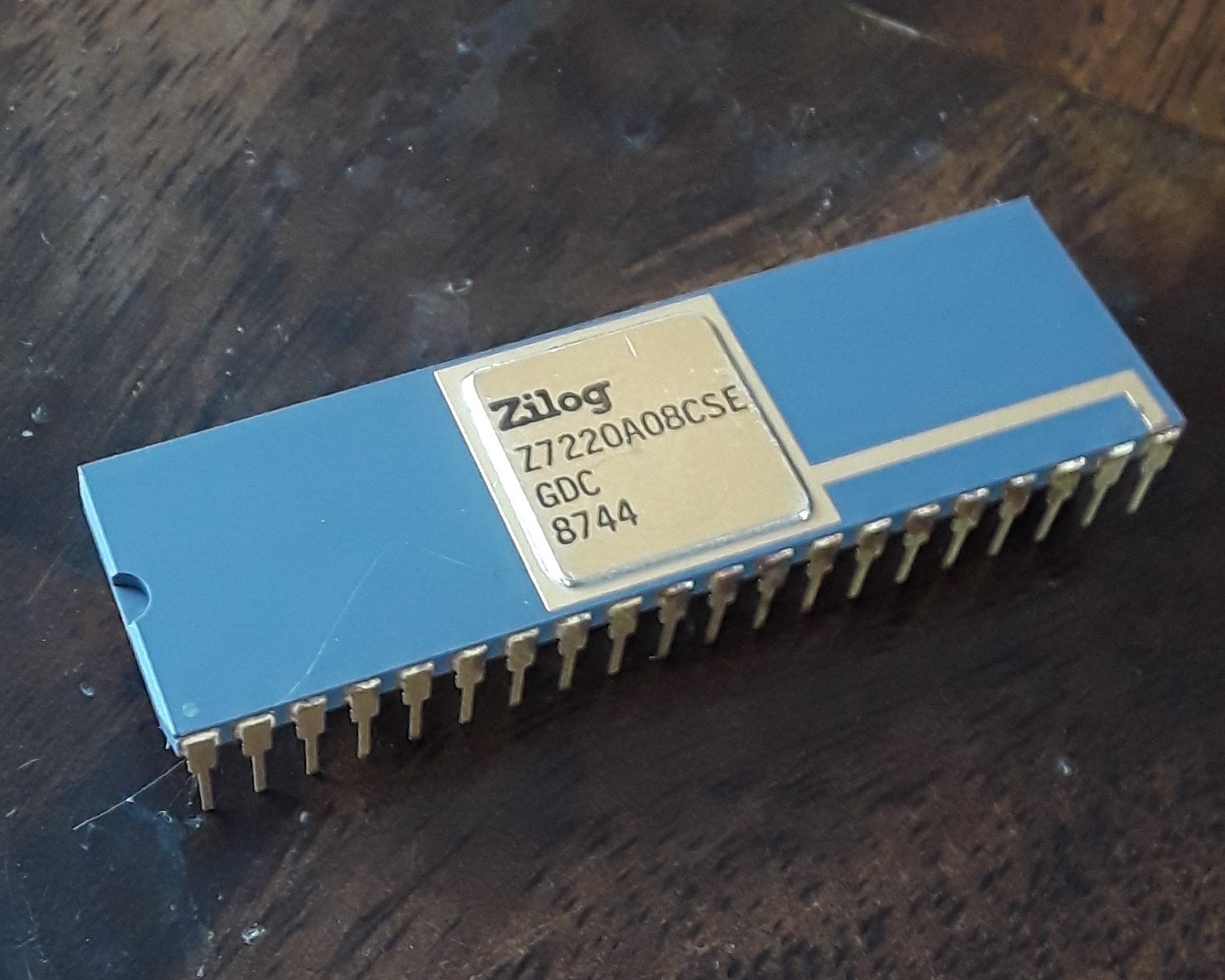
I bought this chip off of Ebay. It seems that Zilog created a uPD7220 clone - and it works! These chips seem to be rather rare and information on them is scarce. I did manage to deduce that there were two variants of chips: one operating at 6Mhz, and one at 8Mhz. I got the 8Mhz one and tried doubling my pixel clock to 16Mhz (the GDC uses a halved clock). That worked too, and that allowed me to make a more stable video signal. I had a problem with the 8Mhz pixel clock where there was not time to output a valid video signal. Now I can output more pixels than I have VRAM for.
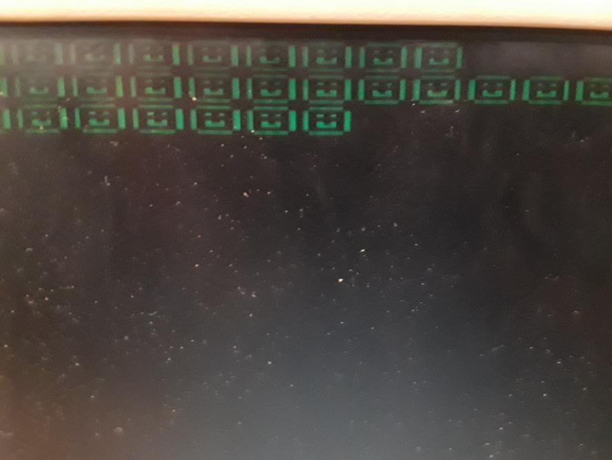
I've managed to make my card render characters! I used the Z80 computer this project was originally intended for this time, instead of the Arduino testbench.
There is not a font yet, so I just rendered a bunch of smiley faces and tested that the program could keep track of the cursor position.
Smiley faces are a good way to do testing.
It's working very well, but I would like to render things a bit faster. I think the Z80 math routines run slow however, for calculating cursor positions and colors.
It doesn't help that my card has 16 colors - it appears that the uPD7220 was designed to just do black and white. This means that I have to send a few more commands to the uPD7220 to select a group of bits for a pixel (multiple colors) instead of just one bit (black and white). The uPD7220 automatically selects a single bit when a command is sent to set the VRAM address, but my program must select multiple.
Over a year ago I wanted a graphics card for my Z80 computer. I made a prototype with the uPD7220, but I never got it working. Until...
As it turned out, I made TONS on mistakes in the original design. There are issues with the new design too, but it works well enough (after a hack, more on that later). Anyway, after playing with the first prototype and trying various hacks, I ended up with a valid VGA signal!
I don't think the uPD7220 was ever supposed to output VGA, considering VGA was introduced about four years after the uPD was, so it's awesome that it can output a VGA signal.
After studying the uPD datasheet and my schematic in depth, I eventually found most of the problems and ended up with my second prototype (which I am using now). I've managed to get it to do the basic things I need it to do. Getting from basic initialization to drawing pixels was very difficult, especially with such a complex device and no example code/libraries, but it was definately worth it. I now want to share what I've learned about it so that more people can use this GDC (GDC = Graphic Display Controller).
I plan on adding more and more information to this project so others can use my work as a reference. I also am going to create a Z80 driver, which I will post here as well.
 Dylan Brophy
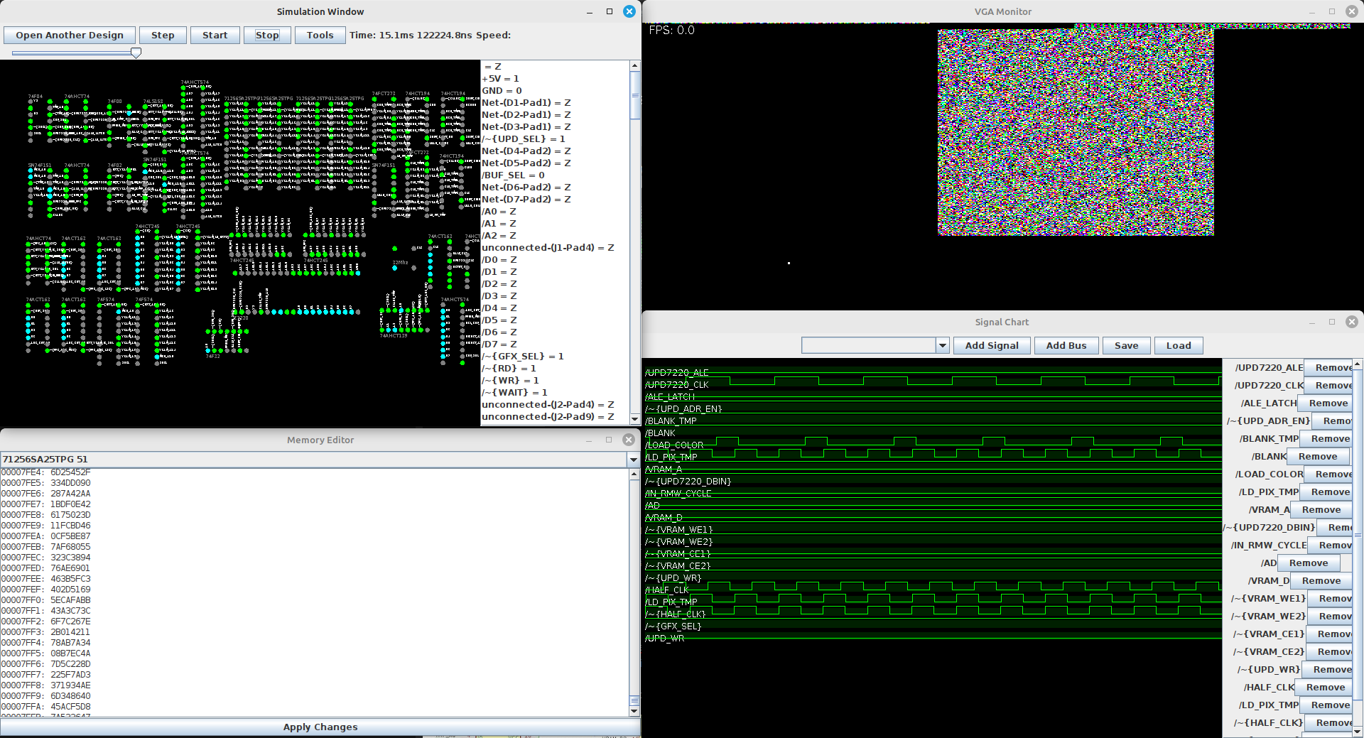 The simulator has some handy features for graphics devices particularly, for example, a VGA display simulator. In the picture, there is a white dot on the VGA display - that is the position of the electron beam at this particular tick. The sim was definitely engineered to my particular use case. Well, I'm pleased with it and hope to use it in projects in the future. Now I can know if a board will work before I order it.
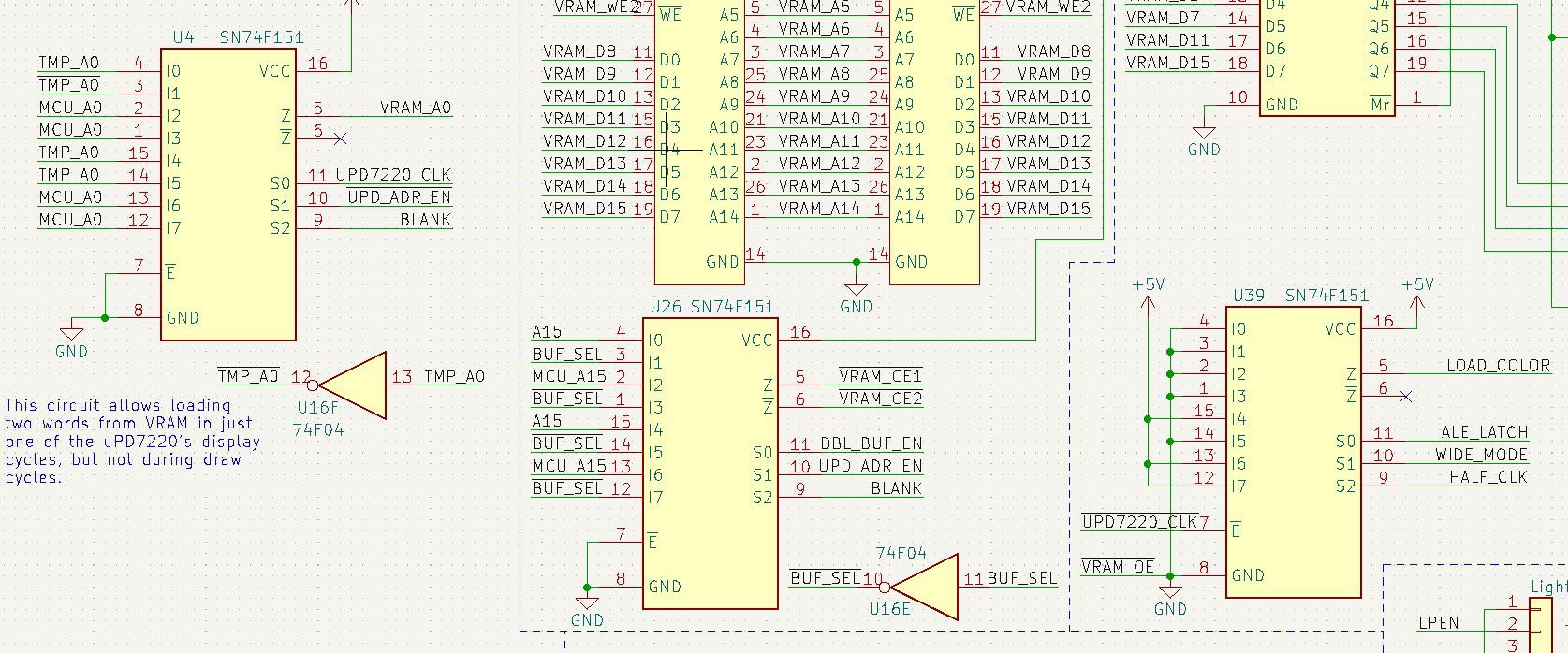
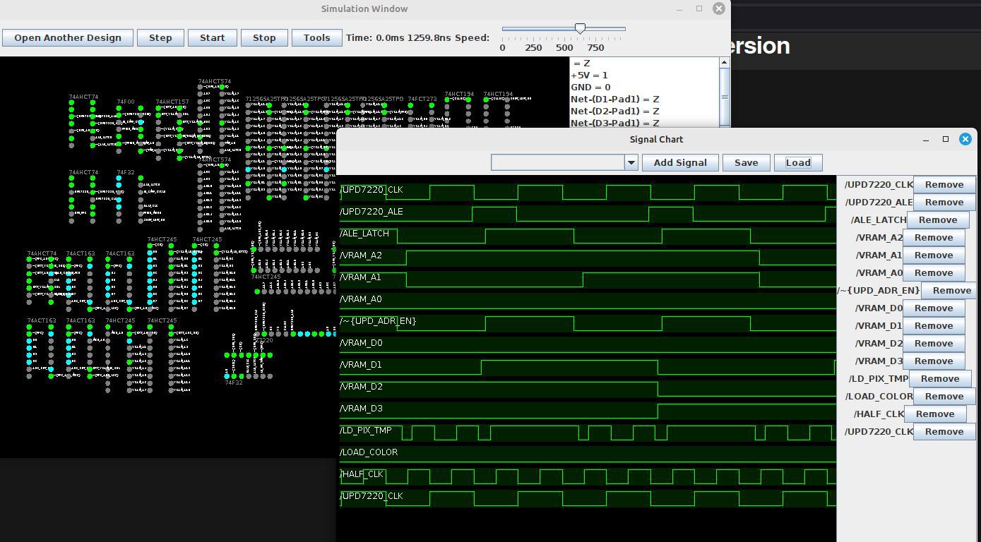 It is VERY alpha, and the library of components is incredibly limited. It has bugs and the UI can crash sometimes. That being said, the simulation itself does not seem to have any problems. It does just one thing extremely well: it simulates the card I'm working on. With some relatively small upgrades it could probably be used to simulate a wide variety of digital circuits.
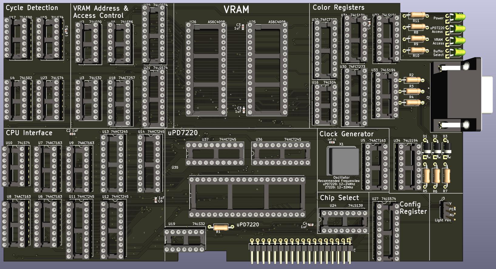 I tried to make the parts of the circuit clearly visible on the board. I also added LEDs, which I typically forget when designing a board. Every board needs blinking lights. Well, I think this board has turned out nicely, at least in the 3D render; it has the clean look I wanted.
 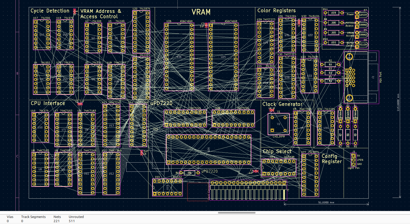 The board now:
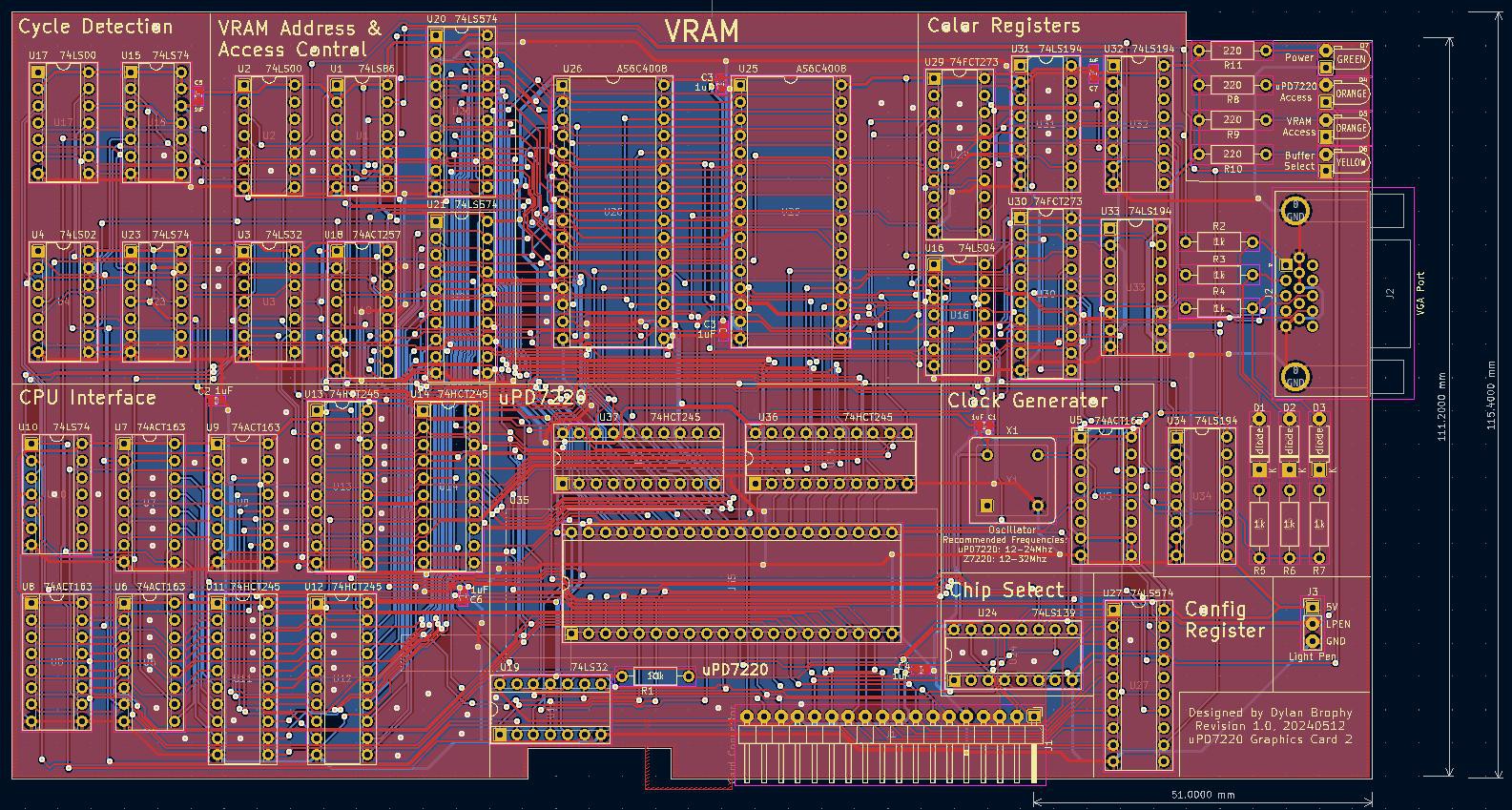 This board was a lot easier to route than I expected. Anyway, expect an update in maybe 10 days when I actually assemble it.
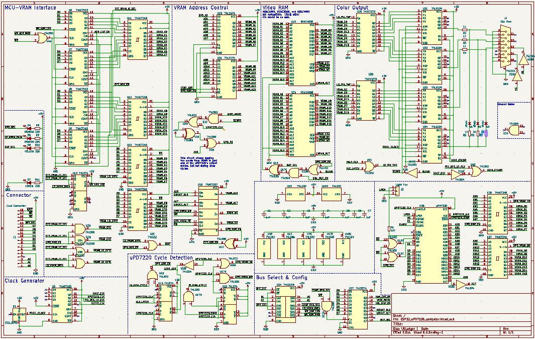 I may add more decoupling capacitors still, but that isn't a real design change. The capacitors are the only SMD components I'm using.
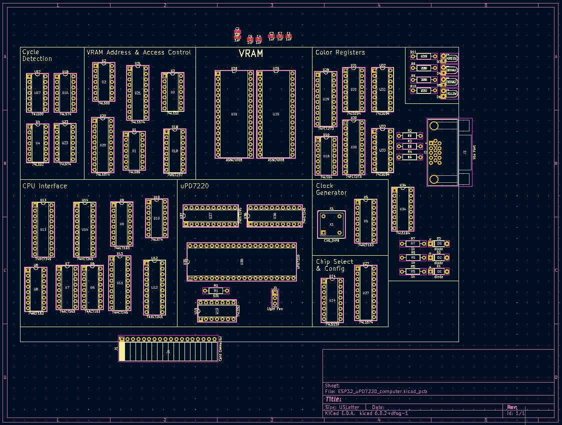 I think I'll also need to make some minor adjustments to the circuit design so the routing is easier, but these are not really functional changes - things like changing the bit order on registers, or rearranging the allocation of gates from chips.
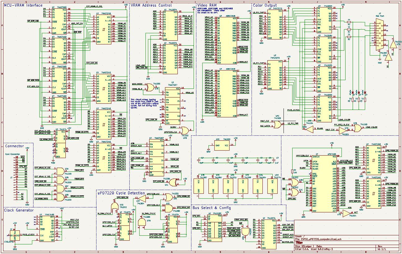 This schematic is way better organized, and hopefully it will still make sense to me 5 years from now. I've added a ton of features since the last board revision, namely:
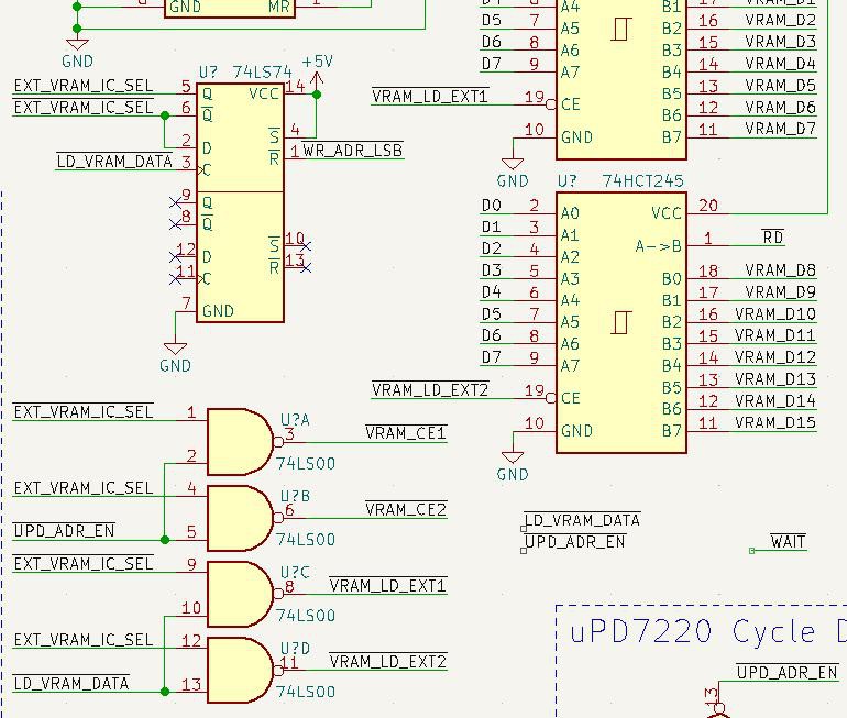 Some of this logic is wrong I think, namely I'm suspicious of the two bottom NAND gates, and I need to add logic for the WAIT line, but this image should give some idea of what the logic is supposed to do. After the main processor writes the lower address byte, the byte-select for the VRAM is reset to zero. Then the processor can write a single byte to the VRAM, which automatically switches the selected byte so the processor can write the other byte. This is done because the VRAM has a 16-bit bus and the processor has an 8-bit bus. Depending on weather the address counting is enabled, the address registers will actually count up to the next word in VRAM, so that the processor can send up to 128KiB of uninterrupted data to VRAM. This is done in-between accesses done by the uPD7220, as the bus is shared, and the uPD7220 gets priority.
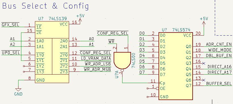 I realize now, looking at this, that I may be able to remove a latch by using A0 for byte select instead of automatically selecting it. Something to think about. Anyway, in the image above you can see that the config register can enable/disable the wide mode logic, control automatic address count, enable or disable double-buffering, to swap buffers, and set A16/A17 for direct VRAM access. The double-buffer enable will make the uPD7220 and processor write to the opposite buffer as the one being displayed, but the buffer still must be manually swapped by the processor.
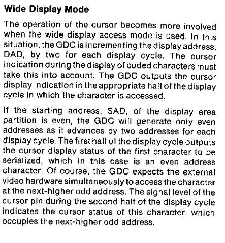
 As it turns out, I don't think I can get it to add 4 instead of just adding two as described above; this limits my maximum clock speed to 24Mhz (32Mhz on the faster Z7220), so the maximum resolution would be limited by this. On the other hand, the uPD7220 supports interlacing, so I might be able to push out a higher resolution that way. Without interlacing under this config, I can't even get to 640x480, but with interlacing I can get at least to 720x480. I'll have to play with the settings.
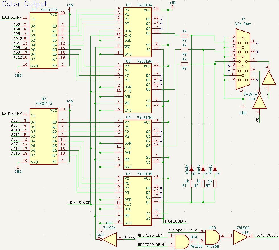
 As a bonus, I'm including a timing diagram from the datasheet so it is easier to find later:
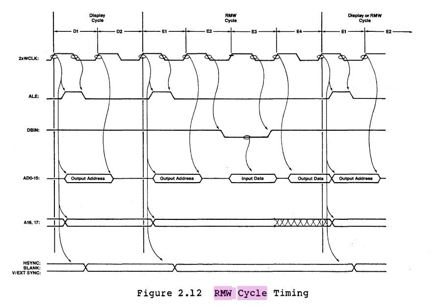 This image details the cycles of various uPD7220 memory accesses, and is super useful for designing the memory control logic.

 I'm not a huge fan of the old board's low resolution. I want at least 640x480, if not higher. Adding more memory for this is quite easy, and in the new schematic this is already handled - the hard part is getting the clock speeds high enough. The uPD7220 can clock at 6Mhz, and the current card gets this by dividing it out of a 12Mhz clock. With a Z7220 the clock is a bit higher, 8Mhz and 16Mhz respectively, but this is nowhere near the pixel bandwidth needed for higher resolutions. My solution to this will be to divide the uPD7220's clock one or two times so we can get 24Mhz or 48Mhz pixel clocks on a uPD7220. That should allow us to get way better resolutions:
 Anyway, I have more stuff to figure out with the board. If any of you have good ideas on the clocks and loading twice the pixels from RAM, let me know :)
 Hopefully my schematics are prettier and more useful this time; I think they will be.